

Page 1

Nakamichi
Service
Manual
Nakamichi
BlackBox
PS-100
SF-1
LA-1
BA-1
MB-1
EC-100
MX-1
00
00
50
50
00
Power Supply
Sub-sonic Filter
Line Amplifier
Bridging
MC
Electronic
Microphone
Booster
Series
Adaptor
Amplifier
Crossover
Mixer
Page 2

CONTENTS
1. PS-100 Power
General, Mute Signal, Specifications,
Supply
Schematic
Diagram, Mounting Diagram
and Parts List, Mechanism Ass'y and Parts List
2.
SF-100
General, Specifications, System Diagram,
Mounting Diagram
3.
LA-100 Line Amplifier ......................................................................................................................................... 8
General, Specifications, System Diagram,
Mounting Diagram
4.
BA-150 Bridging
General, Specifications, System Diagram,
Mounting Diagram
5.
MB-150
General, Specifications, System Diagram,
Mounting Diagram
6.
EC-100 Electronic Crossover ................................................................................................................................
General, Specifications, System Diagram,
Mounting Diagram
7.
MX-100 Microphone Mixer .............• ......
General, Specifications, System Diagram,
Mounting Diagram
Sub-sonic Filter ................•...............................................................................•.....................................•. 5
Schematic
and
Parts List, Mechanism Ass'y and Parts List
Schematic
and
Parts List, Mechanism Ass'y and Parts List
Adaptor
•..........................................................................•........•.......................................•.•...... 11
Schematic
and
Parts List, Mechanism Ass'y and Parts List
MC
Booster Amplifier .............................................................................................................................
Schematic
and
Parts List, Mechanism Ass'y and Parts List
Schematic
and
Parts List, Mechanism Ass'y and Parts List
..
................ ........ ..................
Schematic
and
Parts List, Mechanism Ass'y and Parts List
Diagram,
Diagram,
Diagram,
Diagram,
Diagram,
Diagram,
..
........ .... ........................ .......... .... ..............
1
14
17
20
1.
PS-100
POWER
SUPPLY
General
Power
PS-100
PS-100
power
current:
Although PS-100
nal,
two
Black Box Series make multiple
Supply
is
a regulated
supply for
±200
mA).
input/output
power
supply
unit
the
BiackBox Series (the rated
is
provided only with one
terminals on
the
connection
designed
other
possible.
To
prevent noise signal generation on switching
the
power supply, PS-100 produces a
output
terminals,
of
each
unit
mute
furnished with a
circuit.
Refer
to
Table 1 showing
how
many units
Box Series can be driven by a single PS-100.
Mute Signal
Mute signal
prevent
Power
Transformer
smoothed by
tial
appears
0411
negative
level where
emitter
transient
ON
is
in
the
potential
voltage)
is
muted
output
capacitor
at
C408 (transistor
cutoff
the
for a certain period
noise when
is
rectified through diode
power
is
C408. Therefore, positive poten-
0411
base). Accordingly,
state. C409 (22
through
R414
(1
µF)
Mn),
voltage across C409 exceeds Vbe (base-
of
0412,
0412
turns
from
to
output
output
termi-
units
of
of
PS·
ON/OFF
signal, muting
muting
of
the
Black-
of
time
ON
or
OFF.
D403
is
charged with
therefore
OFF
to
at
be a
the
100
to
and
the
ON.
As
a result,
from+ V to
(The mute time
ON.)
Power
Transformer
with negative
the
voltage across
from
0412
the
acts
power
0413
turns
-10
V,
releasing
depends
OFF
output
OFF
to
is
cut
mute
signal becomes + V (i.e.
to
prevent + V from being
is
OFF.
becomes zero
potential
C408
through
exceeds Vbe
ON and C409
off
and
0413
on and
the
on
C409
is
the
mute
and
R415.
quickly
is
also
Specifications
Maximum
Output
Rated
Dimensions
Weight . . . . . . . . . . . . . . . . . 3.5
Power
Voltage
Output
Consumption
............
Current
..............
. . . 20
± 10 V
. . . . . . . . ± 200
7-1/2(W) x 2-3/8(H)
3-15/16(0)
190(W)
mute
signal
state.
R414
and
so
C408
At
the
of
0411,
discharged.
cut
off.
mute
discharged
VA
mA
inches
x60(H) x 99(0)
lb,
1 .6 kg
is
changed
after
power
is
charged
level where
0411
Therefore
state).
easily
is
turns
Thus,
D402
when
x
mm
1
Page 3

Table 1
Combinations
of
Units Driven by a single PS-100
~
Rating
Combination 4
Maximum
Drivable
Number
of
Units
Schematic
Diagram
1
2
3
5
6
7
PS-100
Power
Supply
4
VA
C±200mAJ
POWER
SF-100
Sub-sonic
Filter
0.5
VA
(±25
mA)
0
0
0
0
B
SUPPLY P.C.B.
LA-100
Line Bridging
Amplifier Adaptor
0.5
VA
(±25mAJ
BA-150
1
VA
(±50
mAJ
0 0
0 0
0
0
0
0
8
4
MB-150
MC
Booster
Amplifier
2
VA
C±100
0
0
0
0
2
mAJ
0402
250235
EC-100
Electronic
Crossover
VA
1
<±50
mAJ
0
0
0
0
4
MX-100
Microphone
Mixer
VA
2
<±100
mAJ
0
0
0
0
2
I
I
+10V
AC
INPUT
12ov-
U.S.A. I CANADA
VERSION
Notes: 1. Fuses
2. The
marked
type
with * 1 are
of
spark killer
.,
r--..,
I
F402
ls30mA,TI
L
__
I
L
marked
I
_J
R417
330K
__
IJAPANVERSlON-
I SP
I I
I I
I I
I I
I I
I
A;~g~
I
L----------·~---_J
not
incorporated
with
-----:,;-,;--;:--,
T~r;,!nal
Fig. 1.1
in
the
*2
differs
YEL
ov
YELi
U.S.A. version.
in
some countries.
2
I
I
0406
2SB435
R411
'
Page 4

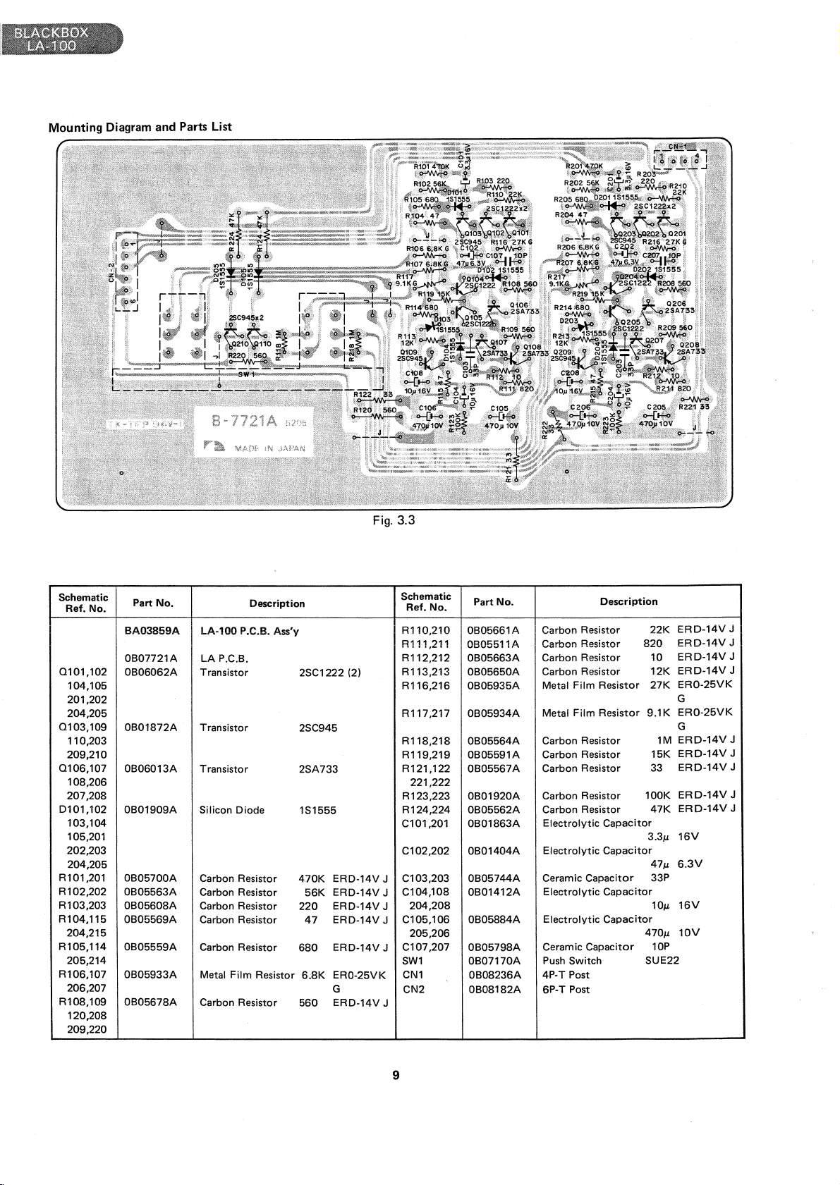
Mounting
Diagram
and
Parts
List
Fig.
1.2
Schematic
Ref. No.
0401,407
408,410
411,412
0402
0403,404
405,409
413
0406
D401
D402,403
ZD401
R401.409
419
R402,408
R403
R404
R405,411
R406
R407
R410.418
R412
R413
R414,416
R415
R417
C401,403
C402,404
Part No.
BA03855A
OB07720A
PS-100 P.C.B. Ass'y
Power
Supply
I OB06013A I T rans1stor
OB01823A
OB01872A
OB06011A
OB06088A
OB01909A
OB06063A
OB01781A
OB05824A
OB05673A
OB05664A
OB05746A
OB01793A
OB05826A
OB01833A
OB05596A
OB05563A
OB05564A
OB05674A
OB01921A
OB01401A
OB01272A
Transistor
Transistor
Transistor
Silicon Diode
Silicon Diode
Zener Diode
Carbon Resistor
Carbon Resistor
Carbon Resistor
Carbon Resistor
Carbon Resistor
Carbon Resistor
Carbon Resistor
Carbon Resistor
Carbon Resistor
Carbon Resistor
Carbon Resistor
Carbon Resistor
Carbon Resistor
Electrolytic
Electrolytic
Description
P.C.B.
Capacitor
Capacitor
2SA733
2SD235 (Y)
2SC945
2SB435
S1RBA
1S1555
YZ040B
1K ERD-25V J
4.7M ERD-50T J
5.6K
ERD-25V
ERD-25V J
3.9K
ERD-25V
ERD-25V J
3.3K
11K
ERD-25V J
10K
ERD-25V J
220K
ERD-25V J
56K
ERD-25V
1M ERD-25V J
820K
ERD-25V
330K
ERD-25V
470µ
25V
100µ
25V
Schematic
J
J
J
J
J
Ref. No.
C405
C406.407
C408
C409
Part
No.
OB01391A
OB01502A
OB01780A
OB05820A
OJ03597B
OE00607A
OE00507A
Description
Electrolytic
Electrolytic
Mylar
Capacitor
Electrolytic
Heat Sink
Screw
M3x8
(3A) (4 pcs.)
Nut
Hex. M3
Capacitor
Capacitor
Capacitor
Philips
220µ
330µ
0.1µ
22µ
(1
pee.)
Pan
Head
(2 pcs.)
25V
16V
50V
16V
(MS)
J
M
3
Page 5
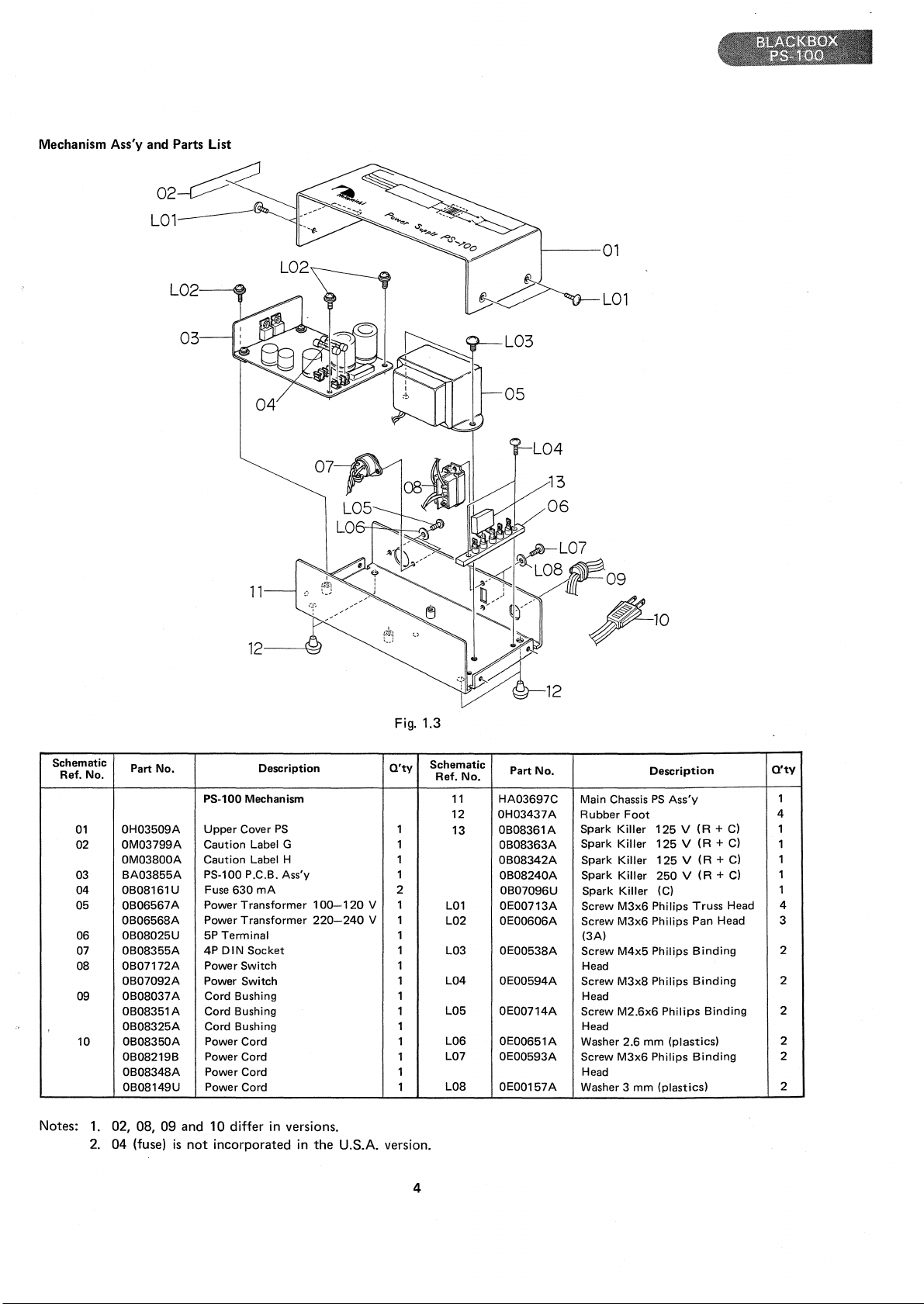
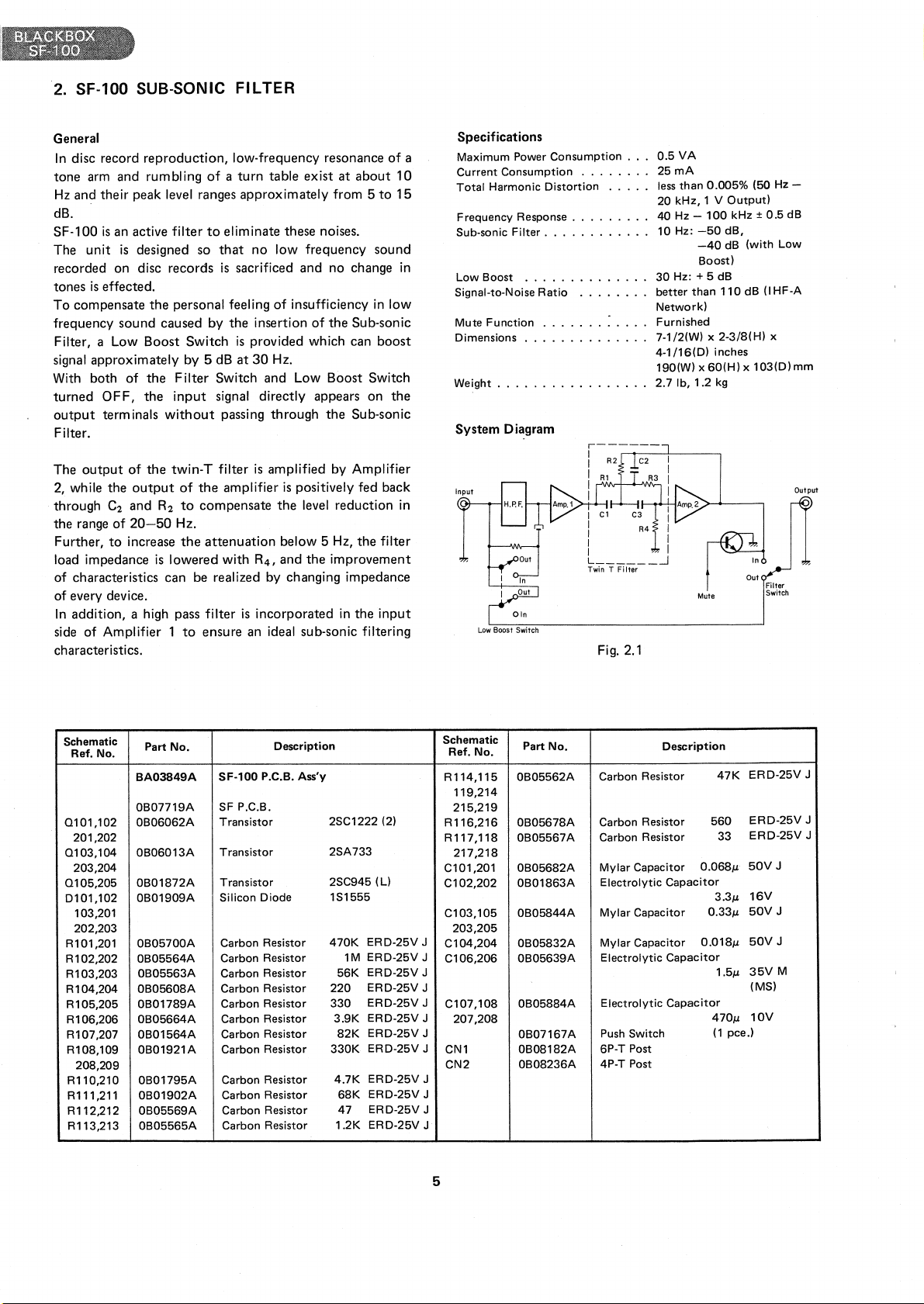
Mechanism Ass'y and Parts List
03
>------01
07
06
Schematic
Ref. No.
01
02
03
04 OB08161U
05 OB06567A
06
07 OB08355A
08
09 OB08037A
10 OB08350A
Notes:
1.
2.
Fig. 1.3
Schematic
Part No.
PS-100 Mechanism
OH03509A
OM03799A
OM03800A
BA03855A
OB06568A Power
OB08025U
OB07172A Power
OB07092A Power
OB08351A Cord Bushing 1
OB08325A Cord Bushing 1
OB08219B
OB08348A Power Cord 1 Head
OB08149U Power Cord 1
Upper
Caution
Caution
PS-100 P.C.B. Ass'y 1
Fuse
Power
5P
4P
Cord Bushing 1
Power
Power
02, 08, 09 and 10 differ
04
(fuse)
is
not
Description
Cover
PS
Label G
Label H 1
630
mA
Transformer
Transformer
Terminal
DIN
Socket 1
Switch
Switch
Cord 1
Cord
incorporated
in
versions.
100-120
220-240
in
the
U.S.A. version.
Q'ty
V 1
V 1
Part
Ref.
No.
11
1
1
2
1
1
1
1
12
13
L01 OE00713A
L02
L03
L04
L05
L06
L07
LOB
No.
HA03697C
OH03437A
OB08361A
OB08363A
OB08342A
OB08240A
OB07096U
OE00606A Screw
OE00538A Screw
OE00594A Screw
OE00714A
OE00651A Washer
OE00593A Screw
OE00157A Washer 3
Main Chassis
Rubber
Foot
Killer
Spark
Spark
Killer
Spark
Killer
Killer
Spark
Killer
Spark
M3x6
Screw
M3x6
(3A)
M4x5
Head
M3x8
Head
M2.6x6
Screw
Head
2.6
M3x6
mm
Description
PS
Ass'y
125 V (R + C)
125 V (R + C)
125 V (R
250 V (R + C)
(C)
Philips
Truss
Philips
Pan Head
Philips
Binding
Philips
Binding
Philips
Binding
mm
(plastics)
Philips
Binding
(plastics)
+ C)
Head
Q'ty
1
4
1
1
1
1
1
4
3
2
2
2
2
2
2
4
Page 6
2.
SF-100 SUB-SONIC
FILTER
General
In
disc record
tone
arm
Hz
and
reproduction,
and
rumbling
their
peak level ranges
low-frequency resonance
of a turn
table
exist
approximately
at
about
from 5
to
of
10
15
dB.
SF-100
The
recorded on disc
tones
To
frequency
Filter, a Low
signal
With
turned
output
is
an active
unit
is
is
effected.
compensate
sound
approximately
both
of
OFF,
terminals
filter
designed so
records
the
personal feeling
caused
Boost
Switch
by 5 dB
the
Filter
the
input
without
to
eliminate these noises.
that
no
low
frequency
is
sacrificed
by
the
is
provided which can
at
30
Switch
of
insufficiency
insertion
Hz.
and
Low
and
of
no
the
Boost
signal directly appears
passing
through
the
sound
change
in
low
Sub-sonic
boost
Switch
on
the
Sub-sonic
Filter.
The
output
2, while
through
the
range
Further,
load impedance
of
the
output
C2 and
of
20-50
to
increase
the
R2 to
is
twin-T
of
the
compensate
Hz.
the
attenuation
lowered
filter
is
amplifier
with R
amplified by Amplifier
is
positively fed back
the
level
reduction
below 5 Hz,
and
the
,
4
the
filter
improvement
of characteristics can be realized by changing impedance
of every device.
In
addition, a high pass filter
side
of
Amplifier 1
to
is
incorporated
ensure
an ideal sub-sonic filtering
in
the
input
characteristics.
in
in
Specifications
a
Maximum
Current Consumption . . . . . . . . 25
Total
Frequency Response
Sub-sonic
Low
Signal-to-Noise
Mute
Dimensions . . . . . . . 7-1/2(W) x
Weight
System
Power Consumption
Harmonic
Boost . . . . . . . . . . . . . .
Function
.................
Distortion
Filter
..
.....
Ratio
. . . . . . . .
. . . . . Furnished
...
Diagram
I I
I I
I . I
L
______
Twin
T Filter
0.5
VA
mA
less
than
20
40 Hz 10 Hz:
30
better
Network)
4-1
190(W)x60(H)x
2.7 lb, 1.2
_J
0.005%
kHz,
1 V
100
-50
-40
Boost)
Hz: + 5 dB
than
/16(D)
I
I
Mute
Output)
dB,
dB
110
2-3/8(H)
inches
kg
(50 Hz -
kHz±
(with
dB (I
103(D)mm
Out
0.5
Low
HF-A
x
Filter
Switch
dB
Output
Fig. 2.1
Schematic
Ref. No.
0101,102
201,202
0103,104
203,204
0105,205
D101,102
103,201
202,203
R101,201
R102,202
R103,203
R104,204
R105,205
R106,206
R107,207
R108,109
208,209
R110,210
R111,211
R112,212
R113,213
Part
No.
BA03849A
OB07719A
OB06062A
OB06013A
OB01872A
OB01909A
OB05700A
OB05564A
OB05563A
OB05608A
OB01789A
OB05664A
OB01564A
OB01921A
OB01795A
OB01902A
OB05569A
OB05565A
Description
SF-100 P.C.B. Ass'y
SF
P.C.B.
Transistor
Transistor
Transistor
Diode
Silicon
Carbon Resistor
Carbon Resistor
Carbon Resistor
Carbon Resistor
Carbon Resistor
Carbon Resistor
Carbon Resistor
Carbon Resistor
Carbon Resistor
Carbon Resistor
Carbon Resistor
Carbon Resistor
2SC1222 (2)
2SA733
2SC945
(L)
1S1555
470K
ERD-25V
1M
ERD-25VJ
ERD-25V
56K
ERD-25V
220
ERD-25V
330
ERD-25V
3.9K
ERD-25V
82K
ERD-25V
330K
ERD-25V
4.7K
ERD-25V
68K
ERD-25V
47
1.2K
ERD-25V
Schematic
Ref.
No.
R114,115
119,214
215,219
R116,216
R117,118
217,218
C101,201 OB05682A
C102,202
C103, 105
203,205
J
C104,204 OB05832A
C106,206
J
J
J
C107,108
J
207,208
J
J
CN1
CN2
J
J
J
J
OB05562A
OB05678A
OB05567A
OB01863A
OB05844A
OB05639A
OB05884A
OB07167A
OB08182A
OB08236A
5
Part
No.
Description
Carbon Resistor
Carbon Resistor
Carbon Resistor
Mylar
Capacitor
Electrolytic
Mylar
Mylar
Electrolytic
Electrolytic
Push
6P-T Post
4P-T Post
Capacitor
Capacitor
Capacitor
Capacitor
Capacitor
Switch
47K
560
33
0.068µ
3.3µ
0.33µ
0.018µ
1.5µ
470µ
(1
pee.)
ERD-25V
ERD-25V
ERD-25V
50V
J
16V
50V
J
50V
J
35V
M
(MS)
10V
J
J
J
Page 7

Schematic Diagram
S.F. P.C.B.
R117
33
r~~:::~
BLK
LEFT
I
OUTPUT
lOUTPUT
Zo•560Sl
RI
•10Kn
,~~::;;
..
RIGHT
OUTPUT
l
OUTPUT
Zo•56on
RI
•10K!l.
Fig.
2.2
2
u
<O
2
u
R118
33
6
Page 8
Mechanism Ass'y
and
Parts List
08
Schematic
Ref. No.
01
02
03
04
05
06
07
08
09
10
L01 OE00713A
L02
Part
OH03507A
BA03849A
OJ03654B
JA03061A
OJ03440A
OB08290B
OJ03277A
OB08355A
OH03508B
OH03437A
OE00593A
No.
10----
~---10
Fig.
2.4
Description
SF·100 Mechanism L03 OE00157A Washer 3
Upper
Cover SF
SF-100 P.C.B. Ass'y
F
rant
Chassis
Push
Button
Switch E Block
6P Pin Jack
Metal Seat
4P
DIN
Main Chassis
Rubber
Screw
Screw
Head
Ass'y
Base
Nut
Socket
SF
Foot
M3x6
Philips Truss Head
M3x6
Philips Binding
O'ty
1
1
1
2
1
1
2
2
1
4
4
2
Schematic
Ref.
No.
L04
L05
L06
L07
LOB
L09
L10
Part
No.
OE00606A
OE00612A Screw
OE00507A
OE00037A Earth Lug B-5
OE00594A Screw
OE00714A Screw
OE00651A
Description
Screw
(3A)
(2A)
Nut
Head
Head
Washer 2.6 mm
mm
M3x6
M3x6
Hex. M3
M3x8
M2.6x6
Philips
Philips
Philips
(plastics)
Pan
Pan
Binding
Philips
(plastics)
Head
Head
Binding
Q'ty
7
2
5
1
1
5
4
4
7
Page 9
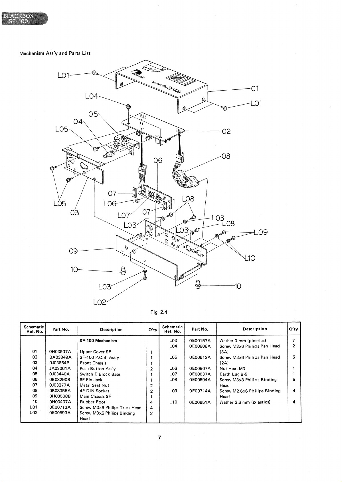
3. LA-100 LINE AMPLIFIER
General
LA-100
may
output
amplifiers
The gain
dB
dB
The
switches
is
an
amplifier with a flat frequency response
be
inserted between amplifiers connected
of a
tape
is
insufficient.
is
selectable
by combination
and 12 dB.
voltage amplification
is
as
follows:
S
:
open,
1
A _ 9.1 k
V(1) - 6.8 k
S
close, S
:
1
2
Av(
S
open,
:
1
A _ ( 1 M + 9.1
3
V(
S
close, S
:
1
4
Av(
deck
or
at
four
of
IN/OUT of
of
:
S
close;
2
//
close;
:
2
9.1 k
//
=
6.8 k //
)
S
open;
:
2
) -
:
open;
2
(1M+9.1k)//27k
=
6.8 k //
)
the
like when the gain of
levels,
0,
+6,
two
gain switches
LA-100
27
27 k
6.8 k
6.8
k
k)
k
6.8
//
at
1
2
27 k
k
each status of
[O
dB]
(6 dB]
that
to
input or
the
+12, and +18
of
the
[ 12 dB]
4
[ 18 dB]
8
Specifications
1
Maximum
Current
Total
Frequency Response .
6
Signal-to-Noise
Reference Level
Input
Output
Mute
Dimensions
Weight
Power
Consumption
Harmonic
Impedance
Level/Output
Function
............
......
Consumption
...
Distortion
Ratio
...
.........
Impedance.
.
.
.
.
.
VA
50mA
0.005%
(20
1 V
Output)
10
Hz -
75
-0.5
dB
better
than
Gain)
Switch 0 dB:
Gain
50
kn
1
V/560
Furnished
7-1
4-1
190(W) x
2.7
n
/2(W) x 2-3/8(
/16(D)
lb,
1.2
Hz -
20
kHz,
kHz+
0,
100
dB
( +
18
1 V
6dB:0.5V
12
dB:
0.25
18
dB:
0.126
H) x
inches
60(H) x 103(D)
kg
dB
V
V
mm
System Diagram
27K
12d8
0
S2
9.1K
Schematic Diagram
LEFT
scu
RIGHT
R223
Fig.
1M
3.1
R122
"
R221
R222
I
Fig. 3.2
8
__
_J
Page 10
Mounting Diagram
and
Parts List
Fig.
3.3
Schematic
Ref. No.
0101,102
104,105
201,202
204,205
0103,109
110,203
209,210
0106,107
108,206
207,208
0101,102
103,104
105,201
202,203
204,205
R101,201
R102,202
R103,203
R104,115
204,215
R105,114 OB05559A
205,214
R106,107
206,207
R108,109 OB05678A
120,208
209,220
Part
No.
BA03859A
OB07721A
OB06062A Transistor
OB01872A Transistor
OB06013A Transistor
OB01909A
OB05700A
OB05563A
OB05608A
OB05569A
OB05933A
Description
LA-100 P.C.B. Ass'v
LA
P.C.B.
Silicon Diode
Carbon Resistor
Carbon Resistor
Carbon Resistor
Carbon Resistor
Carbon Resistor
Film
Metal
Carbon Resistor
Resistor
2SC1222 (2)
2SC945
2SA733
1S1555
470K
ERD-14V
ERD-14V
56K
220
ERD-14V
47
ERD-14V
ERD-14V
680
6.8K
ER0-25VK
G
ERD-14V
560
I Schematic
Ref.
No.
I
R110
210
Part No.
0805661A
Carbon Resistor
I R111 :211 I OB05511A I Carbon Resistor
R112,212
R113,213
R116,216 OB05935A
R117,217
R118,218
R119,219
R121,122
221,222
R123,223
R124,224
C101,201 OB01863A
C102,202
C103,203
J
C104,108 OB01412A
J
204,208
J
C105,106
J
205,206
C107,207 OB05798A
J
SW1
CN1
CN2
OB05663A
OB05650A
OB05934A
OB05564A
OB05591A
OB05567A
OB01920A
OB05562A
OB01404A
OB05744A
OB05884A
OB07170A
OB08236A
OB08182A
J
Carbon Resistor
Carbon Resistor
Metal
Film
Film
Metal
Carbon Resistor
Carbon Resistor
Carbon Resistor
Carbon Resistor
Carbon Resistor
Electrolytic
Electrolytic
Ceramic
Ceramic
Push
4P-T Post
6P-T Post
Capacitor
Electrolytic
Electrolytic
Capacitor
Switch
Description
820
Resistor
Resistor
100K
Capacitor
Capacitor
Capacitor
Capacitor
470µ
SUE22
22K
10
12K
27K
9.1K
1M
15K
33
47K
3.3µ
47µ
33P
10µ
10P
ERD-14V
ERD-14V
ERD-14V
ERD-14V
ER0-25VK
G
ER0-25VK
G
ERD-14V
ERD-14V
ERD-14V
ERD-14V
ERD-14V
16V
6.3V
16V
10V
J
J I
J
J
J
J
J
J
J
9
Page 11

Mechanism Ass'y and Parts List
L01--u;;i..
L05
05
02
08
09
Schematic
Ref. No.
01
02
03
04
05
06
07 OJ03277A Metal Seat
08
09
10
L01
L02
Part
No.
OH03518A
BA03859A
OJ03654B
JA03061A
OJ03440A
OB08290B
OB08355A
OH03519A
OH03437A
OE00713A
OE00593A
Description
LA-100
Mechanism
Upper
Cover
LA-100
Front
Push
Switch E Block
6P Pin Jack
4P
DIN
Main
Rubber
Screw
Screw
Head
LA
P.C.B. Ass'y
Chassis
Button
Ass'y
Nut
Socket
Chassis
LA
Foot
M3x6
Philips Truss Head
M3x6
Philips Binding
Base
Fig. 3.4
O'ty
1
1
1
2
1
1
2
2
1
4
4
2
10
Schematic
Ref. No.
L03
L04
L05
L06
L07
L08
L09
L10
Part No.
OE00157A
OE00606A Screw
OE00612A Screw
OE00594A Screw
OE00037A
OE00714A Screw
OE00651A Washer 2.6
OE00507A
Washer 3
M3x6
(3A)
M3x6
(2A)
M3x8
Head
Earth Lug B-5 1
M2.6x6
Head
Nut
Hex.
Description
mm
(plastics) 7
Philips
Pan
Head 2
Philips
Pan
Head 5
Philips
Binding
Philips
Binding
mm
(plastics) 4
M3
O'ty
5
4
1
Page 12
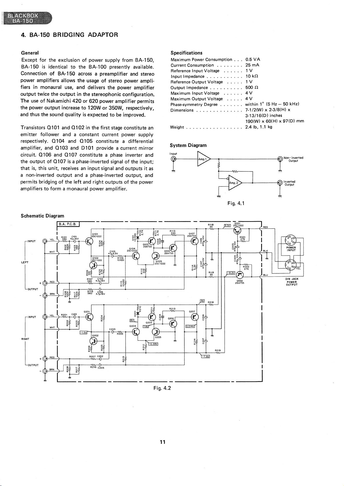
4.
BA-150
BRIDGING
ADAPTOR
General
Except for
BA-150
Connection
the
exclusion of
is
identical
of
to
BA-150 across a preamplifier and
power amplifiers allows
fiers in monaural use,
output
twice
the
output
The use
the
and thus
Transistors
emitter
respectively.
amplifier, and
circuit.
the
that
a non-inverted
perm its bridging
amplifiers
of
Nakamichi
power
output
the
increase
sound
Q 101 and Q
follower and a
Q 104 and Q
0103
Q 106
and
output
of
Q 107
is,
this unit, receives an
output
of
to
form a monaural power amplifier.
quality
and
Q 107
is
the
Schematic Diagram
I B.A. P.C.B.
I
power
supply from BA-150,
the
BA-100 presently available.
the
usage
of
stereo power ampli-
and
in
the
420
or
to
is
102
constant
105
0101
constitute
delivers
620
120W
expected
in
the
power
stereophonic
power
amplifier permits
or
350W, respectively,
to
be improved.
the
first stage
current
constitute
provide a
a phase inverter and
a phase-inverted signal
input
signal and
and
a phase-inverted
left and right
outputs
stereo
amplifier
configuration.
constitute
power supply
a differential
current
of
the
outputs
output,
of
the
mirror
input;
it
and
power
an
as
Specifications
Maximum
Current
Reference
Input
Reference
Output
Maximum
Maximum
Phase-symmetry
Dimensions
Weight
Power
Consumption
Input
Impedance
Output
Impedance
Input
Output
........
.................
System Diagram
Consumption
..
Voltage .
.....
.
Voltage
.....
Voltage .
Voltage
Degree
.
R118
33
Fig.
0.5VA
.
25mA
1 v
10
k.!1
1 v
500
.!1
4V
4V
within
1° (5 Hz -
7-1
/2(W)
x 2-3/B(H) x
3-13/16(D)
190(W) x 60(H) x 97(D)
2.4
lb,
1.1
4.1
inches
kg
50
kHz)
mm
BRN
,,..,,
C203
RIGHT
R209
loo,.,:(~J--'
R216
BRN
C205
Fig.
4.2
11
Page 13

Mounting Diagram
and
Parts
List
z 0
0::
w
Fig. 4.3
...J
w
Schematic
Ref. No.
0001,101
102,104
105,201
202,204
205
0002,103
106,107
203,206
207
0101,201
R001,002
105,205
R101,113
201,213
R102,202
R103,203
R104,204
R106,206
R107,116
207 ,216
R108,117
208,217
R109,115
209,215
R110,111
210,211
R112,212
R
114,214
Part
BA03863A
I
oso109ss
OB06062A
OB06013A
OB01909A
OB05538A
OB01789A
OB05665A
OB05563A
OB05596A
OB05558A
OB05678A
OB01920A
OB05895A
OB01782A
OB05661A
OB01793A
No.
Description
BA-150
I
Carbon Resistor
Carbon Resistor
Carbon Resistor
P.C.B. Ass'y
BA
P.C.B. C003,004
Transistor
Transistor
Silicon
Diode
Carbon Resistor
Carbon Resistor
Carbon Resistor
Carbon Resistor
Carbon Resistor
Carbon Resistor
Carbon Resistor
Carbon Resistor
Metal
Film
Resistor
2SC1222 (2)
2SA733
1S1555
27K
ERD-14V
330
ERD-14V
560K
ERD-14V
56K
ERD-14V
220K
ERD-14V
100
ERD-14V
560
ERD-14V
100K
ERD-14V
10K
ER0-25VK
G
2.7K
ERD-14V
22K
ERD-14V
3.3K
ERD-14V
J
J
J
J
J
J
J
J
J
J
J
Schematic
Ref.
No.
R118,119
218,219
106,107
206,207
C101,201
C102,105
202,205
C103,203
C104,204
Part
OB05567A
I
OB05884A
OB01412A
OB01389A
OB01404A
OB05599A
OE00037A
No.
Description
Caibon Resistor
Electrolytic
Electrolytic
Electrolytic
Electrolytic
Ceramic Capacitor
Earth Lug B-5
Capacitor
Capacitor
Capacitor
Capacitor
33
470µ
10µ
4.7µ
47µ
150P
(1 pee.)
ERD-14V
10V
16V
16V
6.3V
50V
J
12
Page 14

Mechanism Ass'y and Parts List
L01~
05
Schematic
Ref. No.
01
02
03
04
05
06
07
L01
L02
No.
Part
OH03523A
BA03863A
OB08290B
OJ03277A
OB08355A
HA03709A
OH03437A
OE00713A
OE00606A
06
07~
Description
BA-150
Mechanism
Upper Cover
BA-150
6P
Pin Jack 1
Metal
4P
DIN
Main Chassis
Rubber
Screw
Screw
(3A)
BA-150
P.C.B. Ass'y 1
Seat
Nut
Socket 2
BA
Foot
M3x6
M3x6
Ass'y 1
Philips Truss Head
Philips
Pan
Head 4
Fig. 4.4
O'ty
1
2
4
4
Schematic
Ref.
No.
L03
L04
L05
L06
L07
LOB
Part
No.
OE00037A Earth Lug B-5
OE00507A
OE00594A
OE00157A
OE00714A
OE00651A
Nut
Screw
Head
Washer 3
Screw
Head
Washer 2.6
Hex.
M3x8
M2.6x6
Description
M3
mm
mm
Philips
(plastics)
Philips
(plastics)
Binding
Binding
Q'ty
2
1
5
5
4
4
13
Page 15

5. MB-150
MC
BOOSTER
AMPLIFIER
General
MB-150
MC
The gain can
switching the Gain Switch
set
ered
is
a booster amplifier used
type
to
as
cartridge
ON,
the
be
the
input
output
at
selected
low
output
from
without
at
two
ON/OFF.
the
passing
Complementary circuits used
duce distortion.
The first stage
NPN
transistors, with low noise figures
is
composed
of
source impedance, which are
tively
to
ensure low noise figures.
The second stage
configuration
410,
and
input
noise figure
as
630
Equalizing Amplifiers,
adopts
used in
is
less
the
the
than
first stage
-158
Network).
The first-stage transistors have
and PNP. Theoretically, if
types
are
the
same,
the
collector
sistors are equal, and
the
current
voltage across
values
amplification
the
of
+ and - power supply voltage.
circuits, However, a
to
various factors and
zero by offset voltage
their
base
hFE's
input
terminals vanishes
+
or
- voltage slightly remains due
the
voltage should be adjusted
adjustment.
to
increase gain for an
level.
levels
of
38
dB/22
dB
With
the
Pass Switch
cartridge
in
all stages
is
through
directly deliv-
the
amplifier.
of
MB-150
10 PNP transistors and 10
at
small signal
connected
in
parallel respec-
particular triple transistor
of
Nakamichi
and
its equivalent
dB
(with R IAA IHF-A
the
combination
the
characteristics
currents
currents
of
are
of
of
these tran-
the
same if
are equal; therefore d.c.
at
the
identical
In
actual
by
re-
610,
NPN
both
to
Offset Voltage
1.
Insert shorted pin plugs into
2.
Connect a PS-100 power supply
and
Adjustment
turn
the
power
3. Connect an amplifier
to
sound with headphones
4. Adjust semi-fixed
that
switching noises generated
operaton
of
the
pass switch
level.
Specifications
Maximum
Current
Total
Frequency Response . . . .
Equivalent
Ref.
Impedance
Ref.
Maximum
Dimensions
Weight
Power
Consumption
Consumption . . . . . . . . 100
Harmonic
Output
Input
Distortion
Input
Level/Output
........
Level/Input
Input
Level .
......
................
Noise
.......
.
Impedance .
.
input
jacks
of
MB-150.
unit
to
the
MB-150
switch
of
the
PS-100 ON.
to
the
output
or
jacks
a speaker.
and
listen
volumes VR101 and VR201 so
at
the
ON/OFF
reduce
. . . 2
VA
0.005%
0.3 V
20
Hz -
(+
38
10Hz-100kHz+O,
-0.5
-158
Network)
5
mV/5.6
0.4
mV/56
63
µ,V
200
mV
30
mV
7-1/2(W) x 2-3/8(H)
3-15/16(0)
190(W) x
2.9 lb, 1 .3
.
to
mA
(20
Hz - 20
Output)
100
dB
Gain)
dB
(+
22
dB
(RIAA,
.n
.n
/56
.n
(+
22
(+
38
inches
60(H) x 100(D)
kg
a inaudible
kHz,
kHz +
0,
dB Gain)
IHF-A
(+
22
dB Gain)
(+
38
dB Gain)
dB Gain)
dB Gain)
x
-1
dB
mm
System Diagram
-Input
,----
---
-------
--------
--------
-------,
I I
I I
jPass
Pass
Fig. 5.1
I
I
I
I
I
Output
14
Page 16
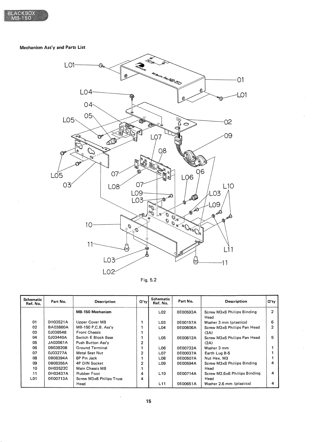
Mechanism Ass'y and Parts List
LOS
09
03
Schematic
Ref. No.
01
02
03 OJ03654B
04 OJ03440A
05
06 OB03920B
07 OJ03277A Metal Seat
08 OB08394A
09 OB08355A
10
11
L01 OE00713A
Part
No.
OH03521A
BA03860A
JA03061A
OH03522C
OH03437A Rubber
10---
Description
MB-150 Mechanism
Upper Cover MB
MB-150 P.C.B. Ass'y
Front
Chassis
Switch E
Push
Ground
SP
4P
Main
Screw
Head
Button
Pin
DIN
Chassis
Block
Terminal
Nut
Jack
Socket
Foot
M3x6
Base
Ass'y
MB
Philips Truss
Fig. 5.2
Schematic
O'ty
Ref. No.
L02
1
1
1
1
2
1
2 L07 OE00037A
1
2
1
4
L03
L04
L05
LOS
LOS
L09
L10
4
L11
Part No.
OE00593A
OE00157A
OE00606A
OE00612A
OE00732A
OE00507A
OE00594A
OE00714A
OEOOS51A
---11
Screw
Head
Washer 3
Screw
(3A)
Screw M3xS
(2A)
Washer 3
Earth Lug B-5
Nut
Hex.
Screw
Head
Screw
Head
Washer 2.6
L10
~
L11
Description
M3x6
mm
M3x6
mm
M3
M3x8
M2.6x6
mm
Phi
lips
(plastics)
Philips
Philips
Philips
Philips
(plastics)
Binding
Pan
Head
Pan
Head
Binding
Binding
O'ty
2
6
2
5
1
1
1
4
4
4
15
Page 17

Schematic Diagram
!INPUT
LEFT
lOUTPUT
llNPUT
RIGHT
lOUTPUT
WHT
BLK
YEL
BLK
BLK
BLU
BLK
RED
(
I
I
I
I
I
I-
I
I
I
I
I
I
I
I
I
I
I
I
I
I
.,1.
~/:
I
I
I
I
I
I
I
....
~~~~~~~~~~
Mounting Diagram and Parts List
0101-0110
.___._~+----+~_._~.___._~..._---+~i--....:..i....J.,,,,...4~
2SA991x10
~
R118
Fig.
5.3
R117
Schematic
Ref. No.
0101-113
Part No. Description
BA03860A
OB07722A
OB06120A
MB-150 P.C.B. Ass'y
MB
P.C.B.
Transistor
2SA991 (26 pcs.)
201-213
R115
!5.6
R116
47K
C112
0.01
0114,214
0115,215
0116-128
216-228
0129,229
VR101,201
R101,201
R102,202
91F
R103,104
203,204
R105,106
OB06062A Transistor
OB01872A Transistor 2SC945
OB06119A Transistor
OB06121A
OB07159A
OB05587A
OB01885A
Transistor
Semi-fixed Volume
Carbon Resistor
Carbon Resistor
OB05511A Carbon Resistor 820
OB01793A Carbon Resistor
2SC1222 (2)
2SC1844 (26pcs.)
2SA990
500
ERD-25V
56
ERD-25V
39K
ERD-25V
ERD-25V
3.3K
J
J
J
J
205,206
R107,108
OB05649A Carbon Resistor 150
ERD-25V
J
207,208
R109, 110
OB05558A
Carbon Resistor
100
ERD-25V
J
209,210
R111,112
OB05545A Carbon Resistor
18
ERD-25V
J
211,212
R113,213
R114,214
R115,215
R116,216
R117,217
OB05661A Carbon Resistor
OB01879A Carbon Resistor
OB05818A Carbon Resistor
OB05562A Carbon Resistor
OB05952A Metal Film Resistor
22K
33K
5.6
47K
91
ERD-25V
ERD-25V
ERD-25V
ERD-25V
ER0-25VK
J
J
J
J
F
R222
¢ I
R118,218
R119,219
R120,220
R121,122
221,222
R123,124
OB05746A Carbon Resistor
OB05854A Carbon Resistor
OB01920A Carbon Resistor 100K
OB05567A Carbon Resistor
OB01833A Carbon Resistor
6.8
33
10K
1
ERD-25V
ERD-25V
ERD-25V
ERD-25V
ERD-25V
J
J
J
J
J
223,224
C101,201
C102,103
OB01914A
OB01289A
Capacitor 3300P
Ceramic Capacitor 220P
50V
50V
Mylar
202,203
C104,105
106,107
OB05884A
Electrolytic
Capacitor
470µ
10V
110,111
113,114
204,205
(TR P.C.B.)
206,207
210,211
213,214
C108,109
208,209
C112,212
SW1
CN1
Fig 5.5
OB01288A
Ceramic Capacitor
100P
OB01290A Ceramic Capacitor 0.01µ
OB07167A
OB08236A
OB08366A Shield
OB07738A
Push
Switch SVE
4P-T
Post
Case
TR
MB
P.C.B.
(2 pcs.)
(2 pcs.)
50V
50V
Fig. 5.4
16
Page 18

6.
EC-100 ELECTRONIC
CROSSOVER
General
EC-100, a
and
output
Each
power
A
combination
to
drive. a 3-way
The
by
combination
an
adder, separates an
and
a low-passed
of
the
two
amplifier
transfer
the
function
formula:
of
a high-pass filter, a phase
input
output.
output
for
of
or
signals
driving a 2-way speaker system.
two
or
more EC-100's makes
4-way speaker system.
GH
(s)
52
GH(s) =
The
transfer function GP(s)
as:
Gp(s)
Further,
The
transfer function
pass filter circuit. Therefore
signal
The
crossover frequency setting
from
Frequency Control VR001.
The
positions
Frequency Control
These frequencies are 66,
370,
5.4
k, 7 k,
the
filters
EC-100 has
band filter circuits; however, in
switching system
systems
nal
tance simultaneously
resistance.
(S+wol2
S-w
0
S+wo
the
added
output
of
lower frequency range.
66
Hz
to
7.4 kHz
Frequency
440,
Control
in
total,
including
and
530,
660,
and
and
7.4 kHz.
is
12
dB/oct.
the
same characteristics
of
EC-100
that
have
....................
of
...................
(Eq. 1 + Eq.
of
Eq. 3 accords with
the
is
is
interlocked at
9 positions
68,
880
The
is
to
change
to
the
shifter
signal into a high-passed
is
delivered
of
a high pass filter
to
a respective
it
possible
is
1
a phase shifter
is
expressed
2
2)
of
the
adder
3
that
of
output
of
of
EC-100
the
adder
at
19
possible by adjusting
19
frequency
10
positions marked
at
the
middle
78, 95, 120, 170,
Hz and 1.4
attenuation
the
k,
characteristic
as
conventional multi-
crossover
or1
of
250,
2.4 k,
frequency
improved from conventio-
the
resistance
system changing
and
only
capaci-
given
is:
a low
is
steps
the
the
them.
320,
3.9
k,
of
the
Specifications
Maximum Power Consumption . . 2
Current Consumption . . . . . . . 100
Attenuation . . . . . . . 12 dB/oct.
Crossover Frequencies .
Distortion . . . • . . . . . . .
Signal-to-Noise Ratio . . . . better than
Ref.
Input
Ref.
Impedance
Maximum
Mute Function
Dimensions
Weight
Level/Input Impedance . 1 V /50
Output
Level/Output
.........
Input
....•..•......
................
• . . • . . . 66, 68, 78, 95,
...
.
.
.
Level
.....
VA
mA
250,320,370,440,530;
660, 880 Hz, 1.4
3.9 k, 5.4
less
than 0.005%
20 kHz)
Network)
kn
V/5600
1
4V
Furnished
7-1/2(W) x 2-3/8(H) x
3-.15/16(D) inches
190(W)
x60(H) x 100(D)mm
2.4 lb,
.
1.1
120,
170,
k,
k,
kg
2.4
7 k, 7 .4
kH~
(20
Hz
110 dB (I HF-A
k,
-
System Diagram
.,._
____
,------------,
I I
I
I ( I
.....
/-
._
__
i _
__,
'>...._.-+---+-------"'__,olum;:.e
I
I High
------,
I
I
I
I
I
, I
_____
Adder
I
_J
____
Mute
(£))
High
Output
Pass
Schematic Diagram
a
I
E.c.
P.c.e.
I
I
2SC900~3
R10S
10
>
~~
~Ii
-tOV
"')!!.:!!..__.(())
r--{'.4).!!b!L.---{41))
Lchl
High Pass
Output
Rchj
Lchl
Low Pass Output
R
chj
Note:
Resistors and capacitors marked with
*will
be
accurate crossover frequencies when frequency
positions.
The standard
value
of
these resistors and capacitors are shown
adjusted in
volume
is
order
to
interlocked
in
the
achieve
at
19
figure.
INPUT
Reh
Fig. 6.2
17
',~
:
\0205
I
I
I
I
! R224
Page 19

Mounting Diagram and Parts List
Fig. 6.3
Schematic
Ref. No.
IC001,101
201
I
I
0101.102
103,201
202,203 R123, 124
0104,204
0105,106
205,206 201,207
0101,102
103,201
202,203
VR001 OB07182A
VR002,003
R101,201
R102,202
R103,203
R104,204
R105,205
R106,206
R107, 117
121,207
217,221
R108,109
208,209
301,302
R110,112
210,212
R111,113
211,213
Part No.
BA03868A
08077398
0806124A
0801910A
0806066A
0801872A
OB01909A
OB07181A
0805700A
OB01564A
0805608A
0805593A
0805606A
0805688A
OB01833A Carbon Resistor
0805663A
0801830A
0805641A
EC-100 P.C.B.
EC
IC
Transistor
Transistor
Transistor
Silicon
Volume
Volume
Carbon Resistor
Carbon Resistor
Carbon Resistor
Carbon Resistor
Carbon Resistor 22
Carbon Resistor
Carbon Resistor 10
Carbon Resistor
Carbon Resistor
Description
Ass'y
P.C.8.
Diode 1S1555
4558
2SC900 (E)
2SD471
2SC945
200K
(C)
10K
(B)
470K
ERD-25V
ERD-25V
82K
ERD-25V
220
ERD-25V
150K
ERD-25V
ERD-25V
390
ERD-25V
10K
ERD-25V
ERD-25V
1.8K
47K
ERD-25V
Schematic
Ref.
R114,115
R116,120
I
I
C101,107
C102,103
202,203
301,302
C104,105
204,205
J
C106,206
J
C108,208
J
J
C109,209 OB01913A
J
CN1,2,3
J
J
J
J
J
No.
118,119
214,215
218,219
122,216
220,222
223,224
Part
0805955A
0805566A
I
I
0805678A
OB01412A
OB05884A
OB05843A
OB05681A
OB01862A
0808236A.
No.
Metal
Film
Carbon Resistor
I
I
Carbon Resistor
Electrolytic
Electrolytic
Mylar
Capacitor
Mylar
Capacitor
Electrolytic
Mylar
Capacitor
4P-T Post
Description
Resistor
560
Capacitor
Capacitor
470µ
0.012µ
0.01µ
Capacitor
1800P
10K
2.2K
10µ
22µ
ER0-25VK
D
ERD-25V
ERD-25V
16V
10V
J
J
16V
J
J
J
18
Page 20
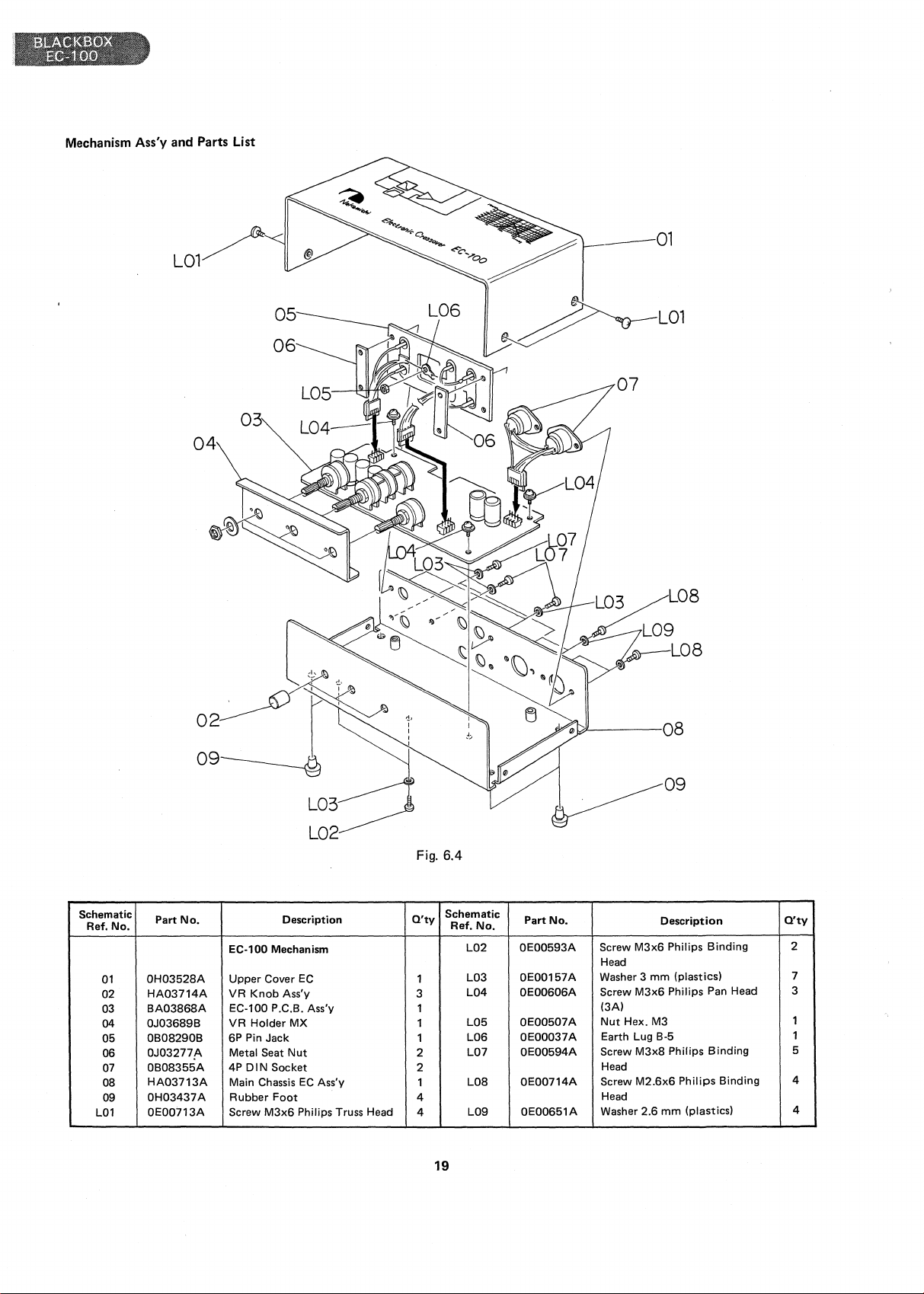
Mechanism Ass'y
and
Parts List
---01
05
03
04
02~
~L01
07
Schematic
Ref. No.
01
02
03
04
05
06
07
08
09
L01
Part
No.
OH03528A
HA03714A
BA03868A
OJ03689B
OB08290B
OJ03277A
OB08355A
HA03713A
OH03437A
OE00713A
09~
EC-100 Mechanism
Upper
VR
Knob
EC-100 P.C.B. Ass'y
VR
Holder
6P Pin Jack
Metal Seat
4P
DIN
Main Chassis
Rubber
Screw
L03~
L02~
Description
Cover
EC
Ass'y
MX
Nut
Socket
EC
Ass'y 1
Foot
M3x6
Philips Truss Head
Fig. 6.4
O'ty
1
3
1
1
1
2
2
4
4
19
Schematic
Ref.
No.
L02
L03
L04
L05
L06
L07
LOS
L09
~09
Part
No.
OE00593A
OE00157A
OE00606A
OE00507A
OE00037A
OE00594A
OE00714A
OE00651A
Screw
M3x6
Head
Washer 3
Screw
(3A)
Nut
Earth Lug B-5
Screw
Head
Screw
Head
Washer 2.6
mm
M3x6
Hex. M3
M3x8
M2.6x6
Description
Philips
Binding
(plastics)
Philips
Pan
Philips
Binding
Philips
mm
(plastics)
Head
Binding
Q'ty
2
7
3
1
1
5
4
4
Page 21

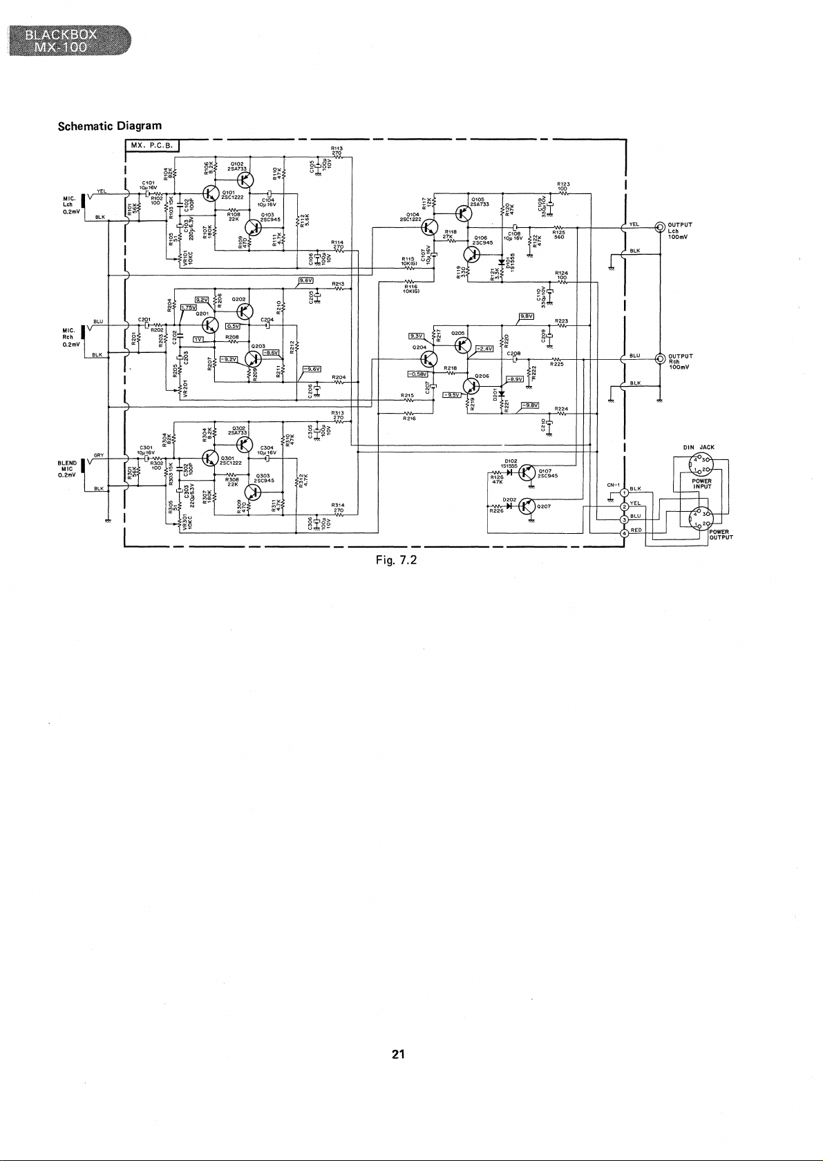
7.
MX-100 MICROPHONE MIXER
General
MX-100
for
use
terminals
to a PA
an Aux.
Further,
is
a mixing
L-channel, R-channel,
as
a simple
on a tape
unit
having three microphone inputs
microphone
deck,
and
Blend.
In
mixer connected
the
unit
allows
addition
(public address) amplifier directly connected
input
of
a preamplifier, etc.
connection
of
this
unit
to
Nakamichi
to
line
the
application
to
input
600
the
cassette console) makes microphone recording by Nakamichi
600
possible.
In
addition,
system, such as Nakamichi 70011, 1000l I
connection
to
the line
input
or
of
500,
a
c~ssette
allows
recording using six microphones.
In
Fig.7.1,
is
given by
the
the
gain of
formula:
the
L-channel microphone amplifier
Av(L)
the
gain
of
and
Av(B)
The
gains
Av(ML) R5/R3 (for L·channel mic. amp.
Av(
MB)
blend microphone amplifier:
=--RY"--"--2
R
of
the
__
+ Rx2 + Ry2
2
_
mixing amplifier:
.............
= R5 /R4 (for Blend mic. amp.
2
output),
output).
to
(a
Therefore the
Av(LO)
Similar
is
mixed
output
= Av(L)
to
the L-channel,
in
the R-channel.
of
the
=:
+ Av(B)
L-channel
the
signal
is
expressed as:
=:
of
blend microphone
Specifications
Maximum
Current Consumption . . . . . . . . 50
Total Harmonic
Input
Input
Output
Maximum
Mute Function . . . . . . . . . . . . Furnished
Dimensions
Weight . . . . . . . . . . . . . . . . . 2.7 lb, 1.2 kg
Power Consumption . . . 1
Distortion
Sensitivity • . . . . . . . . • . 0.2
Impedance
Level/Output Impedance
...........
Input
Level . . . . . . . . 1 V
..............
.....
0.05% (10
1 V
10
..
100
7-1/2(W) x 3-3/S(H) x
4-5/16(D) inches
190(W) x
VA
mA
kHz,
Input)
mV
kn
mV/560
(+
74
dB)
60(H) x 110(D)mm
1 V
Output,
n
System Diagram
Lejt
Blend
Rig It
r-t------1
R1
R2
Mic. L
Volume
Blend Mic.
Volume
Mic.R
Volume
R3
R4
Fig.
7.1
RS
7-----..------t<!JI
Mute
Mute
L Channel
Output
R Channel
Output
20
Page 22
I
R123
<OO
BLEND
MIC
0.2mV
Fig.
R116
10KIG)
7.2
~~!.
R125
N<
N,
ii•
"
o~
Ci§
~~l
~
.
0107
2SC945
560
R124
R224
YEL
OUTPUT
Loh
100mV
BLK
WO
BLU
OUTPUT
Roh
100mV
BLK
DIN
JACK
21
Page 23

Mounting Diagram
and
Parts List
Fig. 7.3
Mechanism Ass'y
L01
and
Parts List
01
~""O-L01
07
Schematic
Ref. No.
0101,104
201,204
Part No.
BA03866A
OB07724A
OB06062A
MX-100
MX
Transistor
Description
P.C.B. Ass'y
P.C.B.
2SC1222 (2)
301
0102,105
202,205
302
0103,106
107,203
206,207
303
0101,102
201,202
VR101,201
301
R101,201 OB05563A
301
R102,123 OB05558A
124,202
223,224
302 201,204
R103,203
303
R104,204 OB01564A
304
R105,205
305
R106,206 OB01878A
306
R107,207 OB05669A
307
R108,208 OB05661A
308
OB06013A
OB01872A
OB01909A
0B07175A
OB05591A
OB05847A
Transistor 2SA733
Transistor
Silicon
Diode
Volume
Carbon Resistor
Carbon Resistor 100
Carbon Resistor
Carbon Resistor
Metal
Film
Resistor
Carbon Resistor
Carbon Resistor
Carbon Resistor 22K
2SC945
1S1555
10K (C)
56K
15K
82K
51
8.2K
180K
ERD-14V
ERD-14V
ERD-14V
ERD-14V
ER0-25VK
F
ERD-14V
ERD-14V
ERD-14V
Schematic
Ref. No.
R109,209 OB01792A
309
R110,120 OB05562A
122,126
210,220
222,226
I
310
I
R111,211
311,312
R112,212 OB05673A
R113,114 OB05645A
213,214
313,314
R115,116 OB05895A
215,216
R117,217
R118,218 OB05538A
J
R119,219 OB01789A
R121,221 OB01793A
J R125,225 OB05678A
C101,104
107,108
J 207,208
301,304
J
C102,202 OB01288A
302
C103,203 OB01394A
303
J C105,106
205,206
J 305,306
C109,110
J 209,210
CN1
Part
No.
OB01795A
OB05650A
OB01412A
OB05885A
OB05841A
OB08236A
Description
Carbon Resistor
Carbon Resistor
I
1
c . R .
Carbon Resistor
Carbon Resistor
Metal
Carbon Resistor
Carbon Resistor
Carbon Resistor
Carbon Resistor
Carbon Resistor
Electrolytic
Ceramic Capacitor 100P
Electrolytic
Electrolytic
Electrolytic
4P-T Post
aroon
Film
es1stor
Resistor
470
4
5.6K
270
330
3.3K
560
Capacitor
Capacitor
220µ
Capacitor
100µ
Capacitor
330µ
47K
""Tl/
·'"'
10K
12K
27K
10µ
ERD-14V J
ERD-14V J
ERD-14V J
ERD-14V J
ERD-14T
ER0-25VK
G
ERD-14V J
ERD-14V J
ERD-14V
ERD-14V
ERD-14V J
16V
6.3V
10V
10V
J
J
J
Schematic
Ref.
01
02
03
04
05
06
07
08
09
L01 OE00713A
No.
Part
No.
OH03526A
HA03714A
BA03866A
OJ03689B
OB03882A
OB08362A
OB08355A
HA03711A
OH03437A
Description
MX-100
Upper
VR
MX-100
VR
Headphone Jack
2P
4P
Main Chassis
Rubber
Screw
Head
Mechanism
Cover
Knob
P.C.B. Ass'y
Holder
Pin Jack
DIN
Socket
Foot
M3x6
MX
Ass'y
MX
MX
Philips Truss
I
o~
Ass'y
~L03
--..___L02
Fig.
Q'ty
1
3
3
1
2
4
4
7.4
Schematic
No.
Ref.
L02
L03
L04
LOS
L06
L07
Part
No. Description
Screw
OE00593A
OE00157A
OE00606A
OE00766A
OE00714A
OE00651A
Head
Washer
Screw
(3A)
Screw
Head
Screw
Head
Washer
TP
M3x6
3 mm (plastics)
M3x6
M3x8
M2.6x6
2.6
Philips
Philips
Philips
mm
Binding
Pan
Binding
Philips
(plastics)
Head
Binding
Q'ty
2
4
3
2
4
4
22
 Loading...