

Nakamichi PDP-42 Service Manual
Service Manual
PDP-42
Plasma Display System
|
|
|
|
|
PDP-42 |
|
|
Plasma Display System |
|
Power |
|
CONTENTS |
|
|
1. |
GENERAL ............................................................................................................. |
2 |
2. |
DISPLAY PANEL ................................................................................................... |
3 |
|
2-1 Location of Major Parts ................................................................................. |
3 |
|
2-2 Removal Procedures ..................................................................................... |
4 |
3. |
VIDEO PROCESSOR / CONTROL UNIT .............................................................. |
6 |
|
3-1 Location of Major Parts ................................................................................. |
6 |
|
3-2 Removal Procedures ..................................................................................... |
6 |
|
3-3 A/D Converter Level Adjustment .................................................................. |
7 |
4. |
MECHANICAL ASS’Y and PARTS LIST (Display Unit) ...................................... |
8 |
5. |
ELECTRICAL PARTS LIST (Display Unit)......................................................... |
11 |
6. |
MECHANICAL ASS’Y and PARTS LIST (Control Unit) .................................... |
12 |
7. |
ELECTRICAL PARTS LIST (Control Unit) ......................................................... |
14 |
8. |
PACKAGE ASS’Y AND ACCESSORY KIT ......................................................... |
17 |
9. |
DESK TOP STAND PARTS LIST ........................................................................ |
17 |
10. |
RECOMMENDED SPAER PARTS LIST ............................................................. |
18 |
11. |
IC BLOCK DIAGRAMS ....................................................................................... |
19 |
12. |
SPECIFICATIONS ............................................................................................... |
27 |
For Schematic Diagrams, and Mounting Diagrams, see the separate volume.
1
1.GENERAL
1.1 Product Code
R535: PDP-42
R554: PDP-42 Display Unit
R555: PDP-42 Control Unit
N935: PDP-42 Accessory Kit
N225: PDP-42 Stand Ass’y
1.2 Destinations
CAN, CH, DA, EP, HK, JPN, OTR, TW, UK, USA,
Abbreviations |
|
CAN - Canada |
CH - China |
DA - South America |
EP - Europe |
HK - Hong Kong |
JPN - Japan |
OTR - Other |
TW - Taiwan |
UK - United Kingdom |
USA - U.S.A. |
1.3 Cautions / Warnings
(1) Product Safety Notice
Parts marked with the symbol  in the schematic diagram have critical characteristics.
Use ONLY replacement parts recommended by the manufacturer. It is recommended that the unit be operated from a suitable DC supply or batteries during initial check-out procedures.
(2) Leakage Current Check / Resistance Check
Before returning the unit to the customer, make sure you make either (1) a leakage current check or (2) a line to chassis resistance check. If the leakage current exceeds 0.5 miliamp, or if the resistance from chassis to either side of the power cord is less than 240 k ohms, the unit is defective.
1.4 Precoutions in Repairing
1.When the base is removed for repair or adjustment, be sure that there are no metal objects in the narrow gap between the P.C.B. assembly or the mechanical part and the base.
2.When soldering the Microprocessor and Video signal processing ICs, use a ceramic soldering iron or a soldering iron whose metal part is grounded since they are not resistant to static electricity.
3.Make sure that wires do not contact heat producing parts.
4.Check that replaced wires do not contact sharp edged or pointed parts.
5.Make sure that foreign object (screws, solder droplets etc.) do not remain inside the set.
1.5 Precautions concerning the DISPLAY PANEL
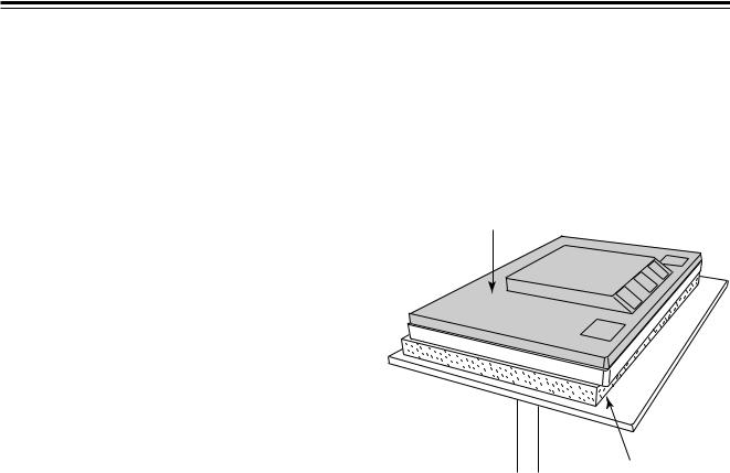
1.Never lay the DISPLAY PANEL directly on a table. Placing the display panel directly on the table may cause serious damage to the DISPLAY TUBE. You must place a sponge pad (or some other soft material) on the table first then place the DISPLAY PANEL on top of the pad.
DISPLAY PANEL
SPONGE PAD
2.Never carry or move the DISPLAY PANEL alone. At least two people should be used to move it. Adding too much stress to the DISPLAY PANEL may cause serious damage to the DISPLAY TUBE. Use extreme caution when handling.
3.As the DISPLAY TUBE is a vaccum tube, never damage the neck (protruding) part of the tube. Use exreme caution when handling (the DISPLAY BLOCK is an extremely expensive piece of equipment).
2

2. DISPLAY PANEL
2-1 Location of Major Parts
DISPLAY TUBE
Fig.2-1 Front View
COOLING FAN |
COOLING FAN |
|
|
|
|
|
COOLING FAN |
|||||||||||||
|
FAN-A PCB |
|
|
FAN-B PCB |
||||||||||||||||
|
|
|
|
|
|
|
|
|
|
|
|
|
|
|
|
|
|
|
|
|
|
|
|
|
|
|
|
|
|
|
|
|
|
|
|
|
|
|
|
|
|
|
|
|
|
|
|
|
|
|
|
|
|
|
|
|
|
|
|
|
|
|
|
|
|
|
|
|
|
|
|
|
|
|
|
|
|
|
|
|
|
|
|
|
|
|
|
|
|
|
|
|
|
|
|
|
|
|
|
|
|
|
|
|
|
|
|
|
|
|
|
|
|
|
|
|
|
|
|
|
|
|
|
|
|
|
|
|
|
|
|
|
|
|
|
|
|
|
|
|
|
|
|
|
|
|
|
|
|
|
|
|
|
|
|
|
|
|
|
|
|
|
|
|
|
|
|
|
|
|
|
|
|
|
|
|
|
|
|
|
|
|
|
|
|
|
|
|
|
|
|
|
|
|
|
|
|
|
|
|
|
|
|
|
|
|
|
|
|
|
|
|
|
|
|
|
|
|
|
|
|
|
|
|
|
|
|
|
|
|
|
|
|
|
|
|
|
|
|
|
|
|
|
|
|
|
|
|
|
|
|
|
|
|
|
|
|
|
|
|
|
|
|
|
|
|
|
|
|
|
|
|
|
|
|
|
|
|
|
|
|
|
|
|
|
|
|
|
|
|
|
|
|
CONNECTION PCB POWER SW PCB FILTER PCB
POWER SUPPLY-2 |
POWER SUPPLY-1 |
REMOTE SENSOR-2 |
PCB |
PCB |
PCB |
Fig.2-2 Front View (under the DISPLAY BLOCK)
3
DISPLAY PANEL
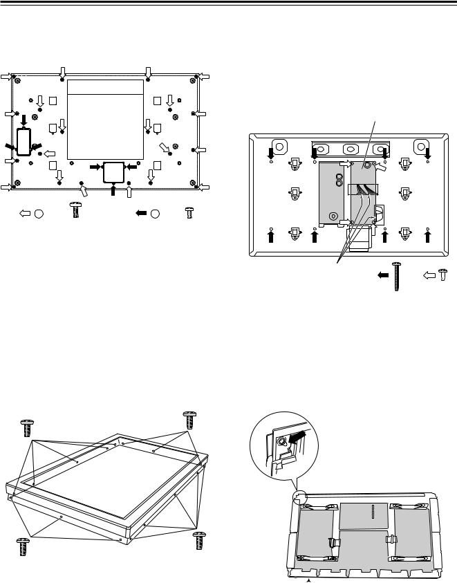
2-2 Removal Procedures
2-2-1. REAR COVER
2-2-3. Removal of the DISPLAY BLOCK
1)Place the DISPLAY PANEL on the sponge pad so that the front is facing down.
2)Remove the 4 retaining screws ( marked) on the left side POWER SUPPLY-2 PCB and move the PCB to remove the 3 connectors on the base.
POWER SUPPLY-2 PCB
: A SCREW |
: B SCREW |
Fig.2-3
(1)Remove the 20 a screws ( marked) on the REAR COVER.
(2)Remove the 6 b screws ( marked) on the REAR COVER.
(3)Carefully remove the REAR COVER from the DISPLAY PANEL.
2-2-2. FRONT COVER
1)Place the DISPLAY PANEL face up on the sponge pad.
2)Remove the 16 retaining screws (top & bottom : 5 each, left & right : 3 each).
CONNECTOR
: : 
Fig.2-5
3)Remove the 8 retaining screws ( marked) that secure the DISPLAY BLOCK.
4)Carefully lift the chassis straight up to remove the DISPLAY BLOCK.
5)If DISPLAY BLOCK replacement is necessary, use extreme caution not to break the protruding part of the DISPLAY TUBE.
Protruding part of the tube
Fig.2-4
3) Carefully lift up and remove the FRONT COVER. |
|
DISPLAY BLOCK |
|
Fig.2-6
4
2-2-4. Reassembling the DISPLAY BLOCK
1) Reassemble in the reverse order for installation.
Special notes before placing the chassis on the DISPLAY BLOCK !
When placing the chassis on the DISPLAY BLOCK, use extreme caution not to break the protruding part of the DISPLAY TUBE as shown in Fig.2-6.
2)When placing the FRONT COVER on the display block, connect the lower side first (taking care to avoid damaging the REMOTE SENSOR-2 PCB), but do not push all the way down yet.
Then connect the upper side of the FRONT COVER to the display block by inserting the two thin metal plates (they look like a pair of bookends) between the chassis and the FRONT COVER (a and b part).
FRONT COVER
A |
B |
CHASSIS OF
DISPLAY BLOCK
Fig.2-7
Next carefully press the upper and lower FRONT COVER until the FRONT COVER completely engages to the chassis of DISPLAY BLOCK.
Cautions:
1)When moving the DISPLAY BLOCK, do not hold the glass section of the DISPLAY TUBE when doing so as this may damage the glass.
2)Please be sure to wipe off any dust that may have collected on top of the DISPLAY TUBE before attaching the FRONT COVER to the DISPLAY BLOCK.
5
3. VIDEO PROCESSOR / CONTROL UNIT
3-1 Location of Major Parts
INLET PCB |
DIGITAL PCB |
POWER SUPPLY PCB |
MAIN PCB |
|
|
|
|
|
|
|
|
|
|
|
|
|
|
|
|
|
|
|
|
|
|
|
|
|
|
|
|
|
|
|
|
|
|
|
|
|
|
|
|
|
|
|
|
|
|
|
|
|
|
|
|
|
|
|
|
|
|
|
|
|
|
|
|
|
|
|
|
|
|
|
|
|
|
|
|
|
|
|
|
REMOTE SENSOR-1 PCB |
|
|
LED PCB |
|
|||||
|
|
|
|
|
|
|
|
|
|
INPUT PCB |
TACT SW PCB |
3-2 Removal Procedures
3-2-1. UPPER COVER
(1)Remove five screws and detach the Upper cover from the unit.
3-2-2. FRONT PANEL BLOCK
(1)Remove the five screws on the bottom.
(2)Disconnect the two flat cables from the P601 & P602 connectors on the INPUT PCB.
(3)Remove the three screws ( marked) on the INPUT PCB.
(4)Release the tabs on both sides snd remove the Front Panel Block by gently pulling it forward. The power button will be disengaged from the Power joint.
UPPER COVER
|
FRONT PANEL |
Release |
Release |
the tab |
the tab |
INPUT PCB
P602 P601
6
VIDEO PROCESSOR / CONTROL UNIT
3-3 A/D Converter Level Adjustment |
|
|
|
|
|
|
|
|
|
|
||||
3-3-1. Y level adjustment |
|
|
|
|
|
|
|
|
|
|
|
|
||
|
|
|
|
|
|
|
|
|
|
|
||||
1) |
Connect a color bar generator (PAL or NTSC) to |
|
|
200mV, 10 S |
|
|
|
|
|
|
|
|||
|
|
|
|
|
|
|
|
|
|
|||||
|
the AV4 composite video input and supply a PAL or |
|
|
|
|
|
|
|
|
|
|
|
|
|
|
|
|
|
|
|
|
|
|
|
|
|
|
|
|
|
|
|
|
|
|
|
|
|
|
|
|
|||
|
NTSC color bar signal (1.0 Vp-p output level, |
|
|
|
|
|
|
|
|
|
|
|
|
|
|
|
|
|
|
|
|
|
|
|
|
|
|||
|
100.0.75.0 colour bars). |
|
|
|
|
|
|
|
|
|
|
|
|
|
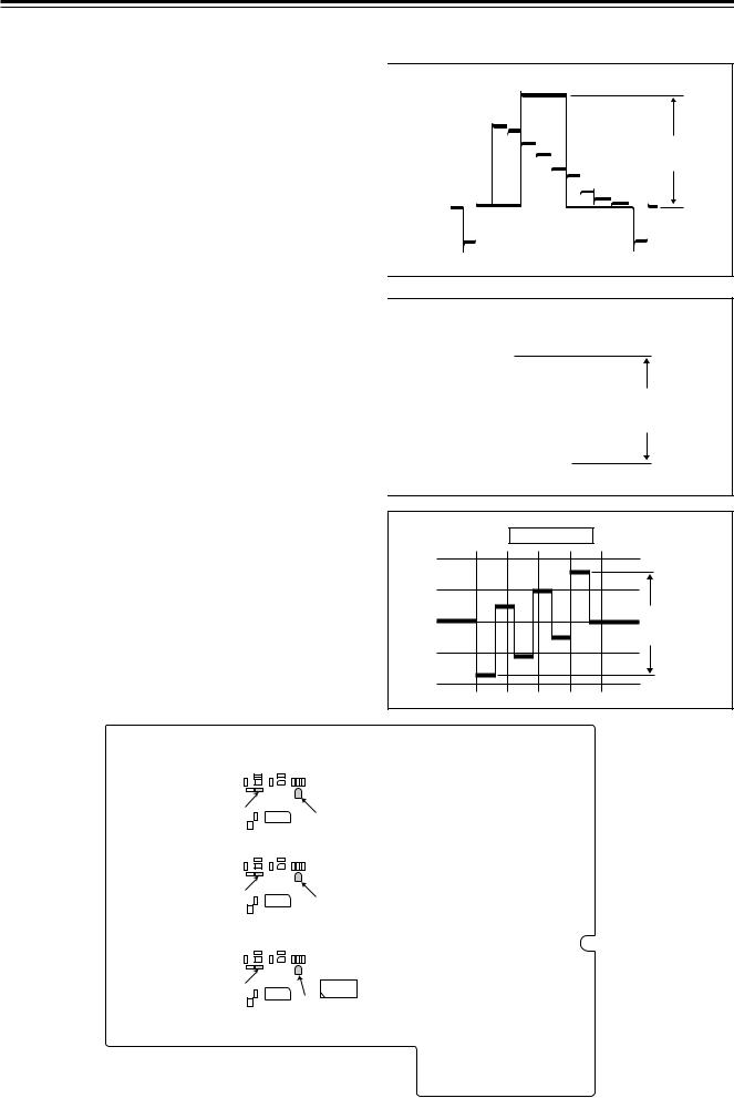
2) |
Connect an oscilloscope to TP41 then adjust VR41 |
|
|
|
|
|
|
|
|
|
|
|
|
|
|
so that the level between the white peak and the |
|
|
|
|
|
|
|
|
|
|
|
|
|
|
|
|
|
|
|
|
|
|
|
|
|
|||
|
pedestal point is 0.86 Vp-p as shown. |
|
|
|
|
|
|
|
|
|
|
|
|
|
|
|
|
|
|
|
|
|
|
|
|
|
|||
|
|
|
|
|
|
|
|
|
|
|
|
|
|
|
|
|
|
|
|
|
|
|
|
|
|
|
|
|
|
|
|
|
|
|
|
|
|
|
|
|
|
|
|
|
<![endif]>0.86V
3-3-2. R-Y level adjustment |
|
|
|
|
|
|
|
|
|
||||||
1) |
Connect a color bar generator (PAL or NTSC) to |
|
200mV, 10 S |
|
|
||||||||||
|
the AV4 composite video input and supply a PAL or |
|
|
|
|
|
|
|
|
|
|
|
|
|
|
|
|
|
|
|
|
|
|
|
|
|
|
|
|
||
|
|
|
|
|
|
|
|
|
|
|
|
|
|
||
|
NTSC color bar signal (1.0 Vp-p output level, |
|
|
|
|
|
|
|
|
|
|
|
|
||
|
|
|
|
|
|
|
|
|
|
|
|
||||
|
|
|
|
|
|
|
|
|
|
|
|
||||
|
|
|
|
|
|
|
|
|
|
|
|
||||
|
100.0.75.0 colour bars). |
|
|
|
|
|
|
|
|
|
|
|
|
|
|
|
|
|
|
|
|
|
|
|
|
|
|
|
|
||
2) |
Connect an oscilloscope to TP81 then adjust VR81 |
|
|
|
|
|
|
|
|
|
|
|
|
||
|
|
|
|
|
|
|
|
|
|
|
|||||
|
|
|
|
|
|
|
|
|
|
|
|||||
|
so that the waveform level is 0.66 Vp-p as shown. |
|
|
|
|
|
|
|
|
|
|
|
|
|
|
|
|
|
|
|
|
|
|
|
|
|
|
|
|
|
|
|
|
|
|
|
|
|
|
|
|
|
|
|
|||
|
|
|
|
|
|
|
|
|
|
|
|
|
|||
|
|
|
|
|
|
|
|
|
|
|
|
|
|
|
|
|
|
|
|
|
|
|
|
|
|
|
|
|
|
|
|
|
|
|
|
|
|
|
|
|
|
|
|
|
|
|
|
|
|
|
|
|
|
|
|
|
|
|
|
|
|
|
|
|
|
|
|
|
|
|
|
|
|
|
|
|
|
|
|
|
|
|
|
|
|
|
|
|
|
|
|
|
|
|
|
|
|
|
|
|
|
|
|
|
|
|
|
|
|
|
|
|
|
|
|
|
|
|
|
|
|
|
|
|
|
|
|
<![endif]>0.66V
3-3-3. B-Y level adjustment
1)Connect a color bar generator (PAL or NTSC) to the AV4 composite video input and supply a PAL or NTSC color bar signal (1.0 Vp-p output level, 100.0.75.0 colour bars).
2)Connect an oscilloscope to TP121 then adjust VR121 so that the waveform level is 0.66 Vp-p as shown.
TP41
VR41
TP121
VR121
TP81
VR81
DIGITAL PCB
200mV, 10 S
Y LEVEL ADJ
B-Y LEVEL ADJ
R-Y LEVEL ADJ
<![endif]>0.66V
7

4. MECHANICAL ASS’Y AND PARTS LIST (Display Unit)
4-1 DISPLAY PANEL Mechanical Ass’y
For main chassis parts list, please refer to Main Shassis Ass’y (A) on page 9 and Main Shassis Ass’y (B) on page 10.
L01 |
6 |
L01
|
|
|
|
|
L01 |
|
|
|
|
|
|
|
|
|
|
L01 |
|
|
|
|
7 |
8 |
L01 |
|
|
|
|
|
|
|
|
|
L02 |
|
|
|
|
|
|
|
|
|
|
|
|
|
L01 |
8 |
7 |
|
|
|
3 |
|
|
|
L02 |
|
|
|
|
|
|
5 |
|
|
|
|
|
|
L01 |
|
|
|
|
|
|
|
|
|
|
|
L01 |
|
|
1 |
|
|
|
|
|
|
|
|
|
|
|
|
L01 |
|
9 |
|
10 |
|
|
|
3 |
|
|
|
|
|
|
|
|
|
|
||
|
|
|
|
2 |
L02 |
|
|
|
|
|
|
|
|
|
|
|
|
|
|
|
|
|
|
|
|
8 |
|
|
|
|
|
|
L03 |
|
L01 |
L01 |
|
|
|
|
|
|
|
|
|
|
L03 |
|
|
|
|
|
4 |
|
|
|
|
|
|
|
|
|
|
L03 |
|
|
|
|
|
|
|
|
|
|
7 |
|
|
|
|
Ref. No. |
Part No. |
Description |
Q'ty |
Ref. No. |
Part No. |
Description |
|
Q'ty |
|
1 |
0H08889A |
P.Flame (C) R554 |
1 |
9 |
0H08894A |
Power Button R554 |
|
1 |
|
2 |
0H08890A |
P.Flame (D) R554 |
1 |
10 |
0J08677A |
Power Button Spring |
|
1 |
|
3 |
0H08891A |
P.Flame (E) R554 |
2 |
L01 |
0E04251A ST |
3x6 + Binding CMT |
|
|
|
4 |
0H08823A |
N.Plate R554 |
1 |
L02 |
0E04257A BT |
3x10 + Binding CMT |
|
|
|
5 |
0B90989A |
Optical Filter PDF-69 |
1 |
L03 |
0E04302A |
TRS40x06SUS BDY |
|
|
|
6 |
0B90990A |
PDP Unit R554 |
1 |
|
|
|
|
|
|
7 |
0H08892A |
Panel Corner R554 |
4 |
|
|
|
|
|
|
8 |
0J08683A |
Angle Panel R554 |
4 |
|
|
|
|
|
|
8
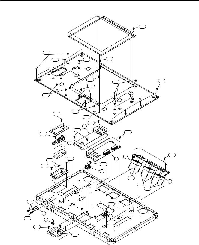
4-1-1 DISPLAY PANEL Main Shassis Ass’y (A)
L04
L05 |
L04 |
L03
L05
L04
L04
L08
L03
L01
1
L01
L03
6
L03
L09
L03
L11 |
|
|
3 |
L10 |
5 |
|
|
|
L07 |
L07
L02
L04
L04 |
L04 |
|
L01
L03
2
1
L12
4
L06
2
L06
L06
L12
4
Ref. No. |
Part No. |
Description |
Q'ty |
|
|
Ref. No. |
Part No. |
Description |
Q'ty |
A-1 |
0B50432A |
P.Supply RPS-8247 |
1 |
|
|
L04 |
0E04276A |
BID40x06STL BNI |
|
|
|
||||||||
A-2 |
0B90988A |
Motor Fan |
3 |
|
|
L05 |
0E04271A |
BID30x06STL BNI |
|
A-3 |
0B85756A |
Inlet ZUG2210-11 |
1 |
|
|
L06 |
0E04280A |
BID40x30STL CMT |
|
A-4 |
0J08674A |
Sapcer Stand |
6 |
|
|
L07 |
0E04251A ST |
3x6 + Binding CMT |
|
A-5 |
0B90984A |
Clamp TL-20S |
1 |
|
|
L08 |
0E04273A |
BID30x08STL BNI |
|
A-6 |
BK10471A |
Filter P.C.B. Ass'y R554 |
1 |
|
|
L09 |
0E04275A |
BID30x12STL BZN |
|
L01 |
0E04278A |
BID40x08STL CMT |
|
|
|
L10 |
0E04285A |
N30STL CMT 3 |
|
L02 |
0E04295A ST |
BID30x05STL BNI |
|
|
|
L11 |
0E04291A |
PW32x080x100NYL |
|
L03 |
0E04251A ST |
3x6 + Binding CMT |
|
|
|
L12 |
0E04283A |
CTS30x06STL CMT |
|
9
 Loading...