

Nakamichi OMS-3A, OMS-3E, OMS-30 Service Manual
~
Nakamichi
Service Manual
Nal<amichi
OMS-3
OMS-3A OMS-3E OMS-30
CONTENTS
1. |
GENERAL . . . . . . . . . . . . . . . . . . . . . . . . . . . . . . . . . . . . . . . . . . . . . . . . |
3 |
|
2. |
REMOVAL PROCEDURES . . . . . . . . . . . . . . . . . . . . . . . . . . . . . . . . . . . . . . |
4 |
|
|
2.1 TOP COVER ASS'YAND BOTTOM COVER ASS'Y . . . . . . . . . . . . . . . . . . . . |
4 |
|
|
2.2 |
SERVO P.C.B. ASS'Y . . . . . . . . . . . . . . . . . . . . . . . . . . . . . . . . . . . . . . |
4 |
|
2.3. |
FRONT PANEL ASS'Y . . . . . . . . . . . . . . . . . . . . . . . . . . . . . . . . . . . . . |
4 |
|
2.4. |
CONTROL&DISPLAYP.C.B.ASS'Y ............................ |
4 |
|
2.5. MAIN P.C.B. ASS'YAND DISC MECHANISM ASS'Y ................... |
4 |
|
|
2.6. |
CHUCK ARM ASS'YAND DISC TRAY ASS'Y ....................... |
5 |
|
2.7. |
LASER PICKUP ASS'Y . . . . . . . . . . . . . . . . . . . . . . . . . . . . . . . . . . . . . |
5 |
|
2.8. |
DISC MOTOR . . . . . . . . . . . . . . . . . . . . . . . . . . . . . . . . . . . . . . . . . . |
5 |
3. |
ADJUSTMENT PROCEDURES . . . . . . . . . . . . . . . . . . . . . . . . . . . . . . . . . . . . |
6 |
|
|
3.1. |
INSTRUMENTS AND GAUGE ................................ |
6 |
|
3.2. PARTS LOCATION FOR ADJUSTMENT .......................... |
6 |
|
|
3.3. |
LASER POWER CHECK . . . . . . . . . . . . . . . . . . . . . . . . . . . . . . . . . . . . |
7 |
|
3.4. VCO ADJUSTMENT ON MAIN P.C.B. ASS'Y . . . . . . . . . . . . . . . . . . . . . . . . |
7 |
|
|
3.5. |
ADJUSTMENT OF SERVO P.C.B. ASS'Y . . . . . . . . . . . . . . . . . . . . . . . . . . |
8 |
|
3.6. |
DISTORTION ADJUSTMENT . . . . . . . . . . . . . . . . . . . . . . . . . . . . . . . . . |
9 |
|
3.7. |
OPERATION CHECK ...................................... |
10 |
4. |
MECHANISM ASS'YAND PARTS LIST ............................... |
11 |
|
|
4.1. |
SYNTHESIS ........................................... |
11 |
|
4.2. |
CHASSIS ASS'Y ......................................... |
12 |
|
4.3. |
FRONT PANEL ASS'Y ..................................... |
13 |
|
4.4. |
TOP COVER ASS'Y....................................... |
13 |
|
4.5. |
BOTTOM COVER ASS'Y.................................... |
13 |
|
4.6. |
DISC MECHANISM ASS'Y................................... |
14 |
|
4.7. |
LOADING GEAR ASS'Y .................................... |
15 |
|
4.8. |
CHUCK ARM ASS'Y ...................................... |
15 |
5. |
MOUNTING DIAGRAMS AND PARTS LIST ............................ |
16 |
|
|
5.1. |
MAIN P.C.B. ASS'Y ....................................... |
16 |
|
5.2. |
SERVO P.C.B. ASS'Y ...................................... |
18 |
|
5.3. |
CONTROL AND DISPLAY P.C.B. ASS'Y .......................... |
20 |
|
5.4. |
HEADPHONE AMP. P.C.B. ASS'Y .............................. |
21 |
|
5.5. |
TERMINAL P.C.B. ASS'Y ................................... |
21 |
|
5.6. |
PHOTO TRANSISTOR P.C.B. ASS'Y............................. |
21 |
|
5.7. |
PHOTO DIODE P.C.B. ASS'Y ................................. |
21 |
6. |
IC BLOCK DIAGRAMS ......................................... |
22 |
' |
7. |
SCHEMATIC DIAGRAM ........................................ |
31 |
|
8. |
WIRING DIAGRAM ........................................... |
32 |
|
9. |
BLOCK DIAGRAM ........................................... |
33 |
|
10. |
SPECIFICATIONS ............................................ |
34 |
|
- 2 -
1.GENERAL
1.1PACKING MATERIALS and OWNER'S MANUAL
The OMS-3/3A/3E/30 is equipped with the Remote Control Unit RM-3CD.
The Remote Control Unit RM-3CD will be supplied per unit as for space parts.
Part No. |
Description |
Q'ty |
OC81618A |
Carton Box OMS-3 |
1 |
OC81614A |
Carton Box OMS-3A |
|
OC81619A |
Carton Box OMS-3E |
|
OC81620A |
Carton Box OMS-30 |
|
OD04640B |
Owner's Manual (English) |
|
OD04642A |
Owner's Manual (Japanese) |
|
OD04641A |
Owner's Manual (English/German/French) |
|
CA80520A |
Remote Control Unit |
|
1.2WARNING
1.2.1IN SERVICE MANUAL
This unit uses an invisible semiconductor laser to pick up the digital signal on the disc. Since the laser can takes the signal without contact, there's no anxiety of rubbing down the disc and the Pickup Ass'y.
But you must treat the laser with the greatest of care. In servicing, please pay attention to the following.
1)Avoid direct exposure to beam.
Laser can be radiated when the interlocks fail or are defeated.
2)Do not break up the Laser Pickup Ass'y.
3)Refered to in itme 2.7 Laser Pickup Ass'y on page 5.
1.2.2LASER SPECIFICATION
The laser provided in the unit is GaAIAs semiconductor laser. The theory of the laser emitting is the same as the light emitting of LEDs. The difference is that the laser has only one wavelength and is coherent.
One of the characteristics of laser diodes is that the threshold level can be changed accordance with the surrounding temperature. To correct this characteristc, the laser diode used in this unit provides a monitor photo diode and controls the output power level of the laser to be constant.
The Laser Pickup Ass'y consists of a laser diode, 6-split photodiode, object lens, beam splitter and coils. The object lens moves forward or back by the focus servo coil and also moves left or right by the tracking servo coil. The laser passes through the prisms and the lenses and is emitted through the object lens. The power of it is decreased to 0.3mW passing through these optical instruments. The laser reflected by the disc passes through the optical instruments again and detected by the 6-split photo diode.
1.2.3CAUTION
Before returning the unit to the customer, make sure you make either (1) a leakage current check or
(2)a line to chassis resistance check. If the leakage current exceeds 0.5 milliamp, or if the resistance from the chassis to either side of the power cord is less than 240k ohms, the unit is defective. WARNING - DO NOT return the unit to the customer until the problem is located and corrected.
1.2.4Main P.C.B
The Main P.C.B. Ass'y C230, C231, C501 - C509, C510, C520, C351, C353, C215, are attached with Sony Bond SC12N.
After replacing any of these components, be certain to apply them with Sony Bond SC12N.
-3 -

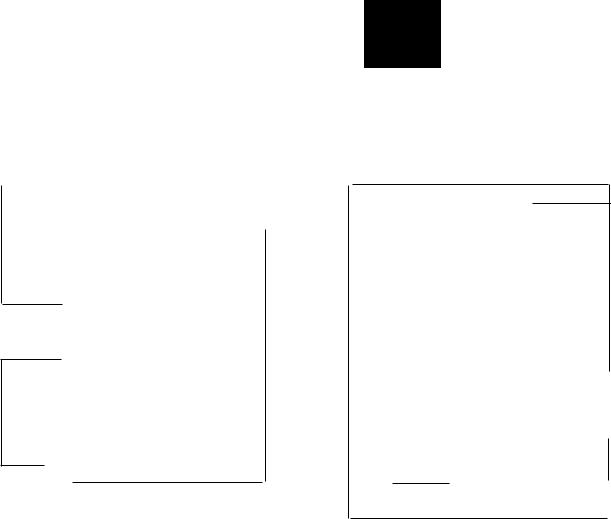
2. |
REMOVAL PROCEDURES |
|
|
2.3. |
Front Panel Ass'y |
|||||
2.1. |
Top Cover Ass'y and Bottom Cover Ass'y |
|
(1) |
Refer to Fig. 2.4 and Fig. 2.5. |
||||||
|
(2) Remove the Top Cover Ass'y and the Bottom Cover |
|||||||||
|
(1) |
Refer to |
Fig. 2.1. |
|
|
|
|
|
||
|
|
|
|
|
|
|
Ass'y refered to in item 2.1. |
|||
|
(2) |
Remove F01 and F02, then lift and remove F03 (Top |
|
|||||||
|
(3) |
Eject the Disc Tray Ass'y and remove F01 (Disc |
||||||||
|
|
Cover Ass'y). |
|
|
|
|
|
|||
|
|
|
|
|
|
|
|
Drawer Cover) by pressing it down with your fingers. |
||
|
(3) |
Remove |
F04, F05, F06 and |
F07, then |
lift and remove |
|
||||
|
|
F08 (Bottom Cover Ass'y). |
|
|
|
(4) |
Remove F02 and F03, then release the latches located |
|||
|
|
|
|
|
|
on both sides of the Chassis. |
||||
|
|
|
|
|
|
|
|
|
|
|
|
|
Front P~ |
Lift F03 |
|
F02 |
(5) |
Remove two connectors (CN-401 and CN-402), then |
|||
|
|
|
fJ |
|
1 |
|
F04 (Front Panel Ass'y). |
|||
|
|
|
|
|
|
|
|
|||
|
|
|
|
|
|
|
|
|
||
|
|
|
.I~, L-f----1 , |
F01 |
|
|
||||
|
|
F02~ |
FOB |
|
|
|
||||
|
|
|
' |
. |
---..:.. q |
|
|
|
|
|
|
|
|
:.____ |
i |
l |
:- l- F04 |
|
|
|
|
F07 ] |
- |
I |
|
|
I
i-F05
Fig. 2.1
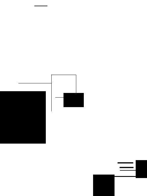
2.2.Servo P.C.B. Ass'y
(1) Refer to Fig. 2.2 and Fig. 2.3.
(2) Remove the Top Cover Ass'y and the Bottom Cover
Ass'y refered to in item 2.1.
F04
(3) Remove F01 and F02 (P.C.B. Support) and five connectors (CN-101, CN-102, CN-103, CN-202 and CN-203), then F03 (Servo P.C.B. Ass'y).
arrows using the index fingers.
Fig. 2.4
~--,,~~~~~F02
~
|
|
|
|
2.4. |
Control & Display P.C.B. Ass'y |
||
|
|
:J_ |
|||||
|
|
|
|
(1) |
Refer to Fig. 2.6. |
||
|
0 |
|
|
|
|
||
|
|
|
|
F01 |
(2) |
Remove the Front Panel Ass'y refered to in item 2.3. |
|
|
|
|
|
|
(3) |
Remove F01, then release the latches located on the |
|
|
|
|
|
|
|
||
|
|
|
|
|
|
|
Front Panel Ass'y, then F02 (Control & Display |
|
|
|
|
|
|
|
P.C.B. Ass'y). |
|
|
|
|
|
|
|
F02 |
|
|
|
|
|
|
|
|
|
|
|
|
|
|
|
|
Fig. 2.2
F03 |
'-F01 |
|
Fig. 2.6 |
2.5.Main P.C.B. Ass'y and Disc Mechanism Ass'y
(1)RefertoFig.2.7.
(2)Remove the Front Panel Ass'y refered to in ite111 2.3.
(3)Remove F03, F05, F06 and F07, then F08 (Main P.C.B. Ass'y).
(4)Remove F09, then F10 (Disc Mechanism Ass'vl.
- 4 - |
Fig. 2.7 |

2.6.Chuck Arm Ass'yand Disc Tray Ass'y
(1)Refer to Fig. 2.8.
(2)Remove the Front Panel Ass'yrefered to in item 2.3.
(3)Remove F01, then F02 (Chuck Arm Plate), F03 (Chuck Arm Spring), F04 and F05 then F06 (Chuck Arm Ass'y).
(4)Remove F07 and F08, then F09 (Disc Drawer Guide L), F10 (Disc Drawer Guide R), thenF11 (Disc Tray Ass'Y).
F01-f
Installing a new Laser Pickup Ass'y
(1)When installing a new Laser Pickup Ass'yyou must connect its three connectors (CN-101, CN-102 and CN-103) to the Servo P.C.B. Ass'yfirst.
(2)Then using a grounded tip soldering iron only, remove the short-circuiting solder in the area of the dotted circle as shown in Fig. 2.1 O; this small P.C.B. which is incorporated with the Laser Pickup Ass'y.
F02 ~ |
'fr--F01 |
r::~4-F02
,fl~F03
F06 |
/c |
|
|
|
F07 |
CAUTON: IF THE SHORT-CIRCUITING SOLDER IS REMOVED BEFORE THE THREE CONNECTORS (CN-101, CN-102 and CN-103) ARE CONNECTED, DAMAGE TO THE LASER DIODE OF THE LASER PICKUP ASS'YCOULD OCCUR IN A MATTER OF SECONDS, CAUSING FAILURE OF THE NEW LASER PICKUP ASS'Y.
NOTE: THE LASER PICKUP ASS'YSTOCKED AS SPARE
PART, MUST BE SHORTED TO DOTTED CIRCLE OF THE SMALL P.C.B. WHICH IS IN· CORPORATED WITH THE LASER PICKUP ASS'YAS SHOWN IN Fig. 2.10.
F09
F11
2.7.Laser Pickup Ass'y (1) Refer to Fig. 2.9.
(2)Remove the Disc Tray Ass'yrefered to in item 2.6.
(3)Remove the three connectors (CN-101, CN-102 and CN-103) from the Servo P.C.B. Ass'y.
(4)Remove F01, then F02 (Laser Pickup Ass'y)along with F03 (Pickup Guide Rail).
NOTE: IF IT IS NOT CERTAIN THAT THE LASER PICK-UP ASS'YIS DEFECTIVE, DO NOT REMOVE THE THREE CONNECTORS (CN-101, CN-102 and CN-103). IF YOU REMOVE THESE THREE CONNECTORS, THE LASER DIODE OF THE LASER PICKUP ASS'YWI LL BE DAMAGED.
0
Fig. 2.10
2.8.Disc Motor
(1)Refer to Fig. 2.11.
(2)Remove Disc Tray Ass'yrefered to in item 2.6.
(3)Remove F01, then pull up F02 (Turntable B Ass'y)
(4)Remove F03, then F04 (Disc Motor).
F02
Fig. 2.11
RE·ASSEMBLY OF THE DISC MOTOR:
(1)Refer to Fig. 2.12.
(2)When re-assembling the Disc Motor, adjust the hei1ht of the turntable using the Turntable Adjustment Gauge (OC82258A).
Turntable
Turntable Adjustment Gauge.
- 5 -
Fig.2.12
3.ADJUSTMENT PROCEDURES
3.1Meters and Gauge
(1)Oscilloscope (15 MHz or more)
(2)AC Voltmeter
(3)DC Voltmeter
(4)Optical Power Meter
(5)Phillips Test Sample Disc 5/5A
(6)Sony Test C.D. Type III (YEDS-7)
(7)Frequency counter
(8)Distortion Meter
(9)Turntable Adjustment Gauge (Fig. 3.1)
3.2Parts Location for Adjustment
@ |
0 |
0 0 |
0 |
@ |
|
VRIOl |
|
TP102 |
TPIOI |
VR104 |
|
|
(GND> |
IFocu1) |
|||
Tr1Ck1ng Ge1n |
T,.;lung |
||||
|
|
||||
|
TP104 |
TPlOJ |
|
Ottwt |
|
|
!Kick PuiNI |
fTrac:k1ngl |
|
||
0
TP1011CN'Ol
0 |
II |
VRlOI |
|
||
qPI08 |
~ |
Foc1.11 OffNt |
r-<J tTr.:k•nt Error) |
||
I TP106 |
JI |
VRHl'2 |
~"° |
~ |
E-F= S.19"CI |
TPI~
RIM |
Q TPI09 |
~ |
|
|
|
|
Q TPl!O |
NOTE: The above Semi-fixed VR positions are for initial presetting.
Turntable Adjustment Gauge (OC82258A)
Fig. 3.1
Main P.C.B.
|
|
l.201 Q TP2041GNO> |
|
0 ie';~s;gnou |
0 TP20J ~ |
|
|
9P202 I YM3811 |
|
s |
|
<GNO> ..______ Q |
|
||
|
|
TP2051VCO Frequenevl |
|
|
|
@oTPJOI |
|
|
|
VRJOI |
|
?..o 7516 |
0 TN02 IMPU Anet |
T•rm1MIJ |
|
|
|
||
QTP•OH+SVl
Fig. 3.2
- 6 -
3.3Laser Pickup Laser Power Check
(1)Remove the Top Cover Ass'y refered to in item 2.1 on page 4.
(2)Short-circuit TP105 and TP106 located or:i the Servo P.C.B. Ass'y.
(3)Place the optical power meter against the pickup (Fig. 3.3), and check that the laser power is between 0.15mW and 0.4mW.
Optical Power Meter
=~
Lens of Pickup Ass'y
Turntable
Fig. 3.3
00000
000
KSS-1238 |
|
|
lop |
0 |
0 |
0 |
|
|
|
Indication |
|||
|
|
|
|
|
|
|
|
|
|
|
10s |
1s |
Decimal |
|
|
|
|
|||
|
|
|
|
place |
place |
place |
|
|
|
|
|||
|
|
|
|
Units: mA; decimal places ommitted |
||
|
|
|
Laser Pickup Current Indication |
|||
|
|
|
|
|
||
|
Fig. 3.4 Location of Laser Pickup Nameplate |
|
||||
3.4Adjustment of VCO on Main P.C.B. Ass'y
3.4.1 VCO Frequency Adjustment (OMS-4 is No signal.)
(1)Connect the frequency counter to TP205 (VCO Frequency) and TP204 (GND).
(2)Remove CN-203 connector cord, turn the power switch on, and short-circuit TP201 and TP202.
(3)Rotate the L201 core and adjust so that the frequency counter shows a value of 4.322MHz.
(4)After adjusting, turn the power off and connect the CN-203 connector cord.
Frequency Counter
I I
Fig. 3.5
- 7 -

3.5Adjustment of Servo P.C.B. Ass'y
3-5-1 Setting of initial position of the semi-fixed volume Before adjusting, preset all semi-fixed volumes are their mechanicall center (VR101, 102, 103, 104).
3.5.2Tracking Offset Adjustment
(1)Rotate VR103 fully clockwise.
(2)Short circuit TP105 and TP106, and without inserting a disc adjust VR104 so that the voltage
of TP103 (Tracking Coil Output) and TP102 (GND) is 0 ± 5mV.
(3)Disconnect TP105 and TP106, then preset VR103 to mechanical center.
3.5.3Focus Offset Adjustment
(1)Connect a DC voltmeter across R184 (120.Q) on Servo P.C.B. Ass'y.
(2)Short circuit TP105 and TP106 (Laser Power On) on Servo P.C.B. Ass'y.
(3)Turn the power switch on, and calculate the cur·
rent from voltage on both ends of R184, and check that the difference compareted to the laser pickup indication (Fig. 3.6) is within ±10% for the negative side. Next turn the power switch off and disconnect the AC voltmeter.
(4)Turn the power back on, set the Philips Test Sample 5 test disc, and observe the TP201 output waveform (EFM signal).
(5)Adjust the VR101 so that the EFM signal level becomes high and the waveform becomes distinct, so that the lines are not thick (Fig. 3.6).
!
T
' 0i .5V/d1V r---~-n-===._~~--;.~_;__~__:~~,.....AL
:
Focus Offset VR (VR101) Adjustment
:
Focus Offset VR (VR 101) at Maximum (Level is high but waveform is unclear)
!
t
Focus Offset VR (VR101) at Minimum (Level is low and wavefrom is unclear)
Fig. 3.6 Focus Offset VR EFM Signal Waveforms
- 8 -
\
3.5.4E-F Balance Adjsutment (Supplementary Beam Balance Adjustment)
(1)Turn the power off and use a 1Ok.Q resistor to short TP105 and TP106.
(2)Connect the oscilloscope between TP201 (EFM signal) and TP202 (GND), and also between TP108 (Tracking Error) and TP107 (GND).
(3)Turn the power switch, load the Philips Test Sample 5 test disc and playback from the first selection.
(4)Connect TP402 (MPU Reset Terminal) and TP401 (+5V) on the Main P.C.B. Ass'y.
(As the microprocessor is in the Reset mode, the LED does not light)
(5)Rotate VR103 (Tracking) fully clockwise.
a)Oscilloscope Ranges
b)Voltage Range (AC): CH1 .... 1V
CH2 .... |
2V |
c)(Set trigger on CH2)
d)Sweep Range: 1mS
(6)Observe the trakcing error waveforms (Fig. 3.7) and adjust VR102 so that the GND line is positioned at exactly half the waveform P-P value.
(7)Turn the power switch off, disconnect the oscilloscope, TP401 (+5V) and TP402 (MPU Reset terminal), and set VR103 to the mechanical center.
EFM signal output |
lmS |
|
,......_ |
|
l 50% |
1+-..,._-iw-+-._.._ _,'""""-++..... |
+-++-+H~~-1 50%GND Line |
~Tracking Error Output
Fig. 3.7
3.6DISTORTION ADJUSTMENT
(Adjust after the Servo P.C.B. adjustment has been completed) Play the 20th selection on the Sony Type III test disc (1KHz - 60 dB). Connect the L.P.F. (20 kHz) to the AC voltmeter and the distortion
meter.
Adjust the VR301 so that distortion in the 3% range is as low as possible.
>Dynamic range is greater than 91 dB.
<Check to make sure that distortion is below 0.0085%.
3.5.5Tracking Gain Adjustment
(1) Load the Philips Test Sample 5 test disc (nonscratched), observe the noise voltage on the voltmeter, and adjust VR103 so that the noise voltage on TP103 (Tracking) and TP102 (GND) is 0.26V RMS ±0.01V (Fig. 3.8).
|
|
|
|
|
|
|
|
|
|
|
|
|
|
|
|
|
|
|
|
|
|
|
|
|
|
|
|
|
|
|
|
|
-- |
- |
|
|
>--- |
|
f -- |
|
|
|
|
|
|
|
|
|
|
|
|
|
|
|
|
|
|
|
|||||
|
|
|
|
|
|
|
|
|
|
|
|
|
|
|
|
|
|
|
|
|
|
|
|
|
|
|
|
|
|
|
|
|
|
|
|
|
|
|
|
|
|
|
|
|
11 - ~ |
-J |
1.- - |
|
I |
|
.I |
lo I. |
|
|
|
|
I |
||||||
|
|
|
|
|
|
|
|
|
|
|
|
|
|
|
|
.,... |
|
|
~..-"' |
|
|
|
|
|
|
|
|
||||
|
~~·. |
|
' .1.ll |
|
•r |
|
' |
|
|
~l!W |
|
·- |
|
|
|
|
I~ |
||||||||||||||
|
|
|
|
|
|
|
|
|
|
||||||||||||||||||||||
|
|
|
|
|
|
|
|||||||||||||||||||||||||
|
|
|
|
|
|
|
|
|
|
|
|
|
,, |
|
|||||||||||||||||
|
r•.. |
|
|
|
|
|
|
|
|
|
|
|
|
|
|
|
|
|
|
|
|
|
,._ |
|
|
|
|
||||
|
|
|
•"" |
|
|
|
|
|
|
|
I |
|
,I,~'•·.> |
|
''.t.,i |
|
.••.J~. |
|
|
|
|||||||||||
|
., |
|
II |
I |
f I' r |
..,... |
|
|
'f' |
|
I T I~· |
|
'If |
'1 r |
|
|
|
|
|
II I |
|
||||||||||
|
|
|
|
|
|
|
|
|
|
|
|
|
|
|
|
|
|
|
|
|
|
|
|
|
|
|
|
|
|
|
|
|
|
|
|
|
|
|
|
|
|
|
|
|
|
|
|
|
|
|
|
|
|
|
|
|
|
|
|
|
|
|
|
|
|
|
|
|
|
|
|
|
|
|
|
|
|
|
|
|
|
|
|
|
|
|
|
|
|
|
|
|
|
|
|
|
|
|
|
|
|
|
|
|
|
|
|
|
|
|
|
|
|
|
|
|
|
|
|
|
|
|
|
|
|
|
|
|
|
|
|
|
|
|
|
|
|
|
|
|
|
|
|
|
|
|
|
|
|
|
|
|
|
I |
|||||
|
|
|
|
|
|
|
|
|
|
|
|
|
|
|
|
|
|
|
|
|
|
|
|
|
|
L- |
|||||
|
|
|
|
|
|
|
|
|
|
|
|
|
|
|
|
|
|
|
|
|
|
|
|
|
|
|
|
|
|
|
|
|
|
|
|
|
|
|
|
|
|
|
|
|
|
|
|
|
|
|
|
|
|
|
|
|
|
|
|
|
|
|
|
|
|
|
|
|
|
|
|
|
|
|
|
|
|
|
Fig. 3.8 |
|
|
|
|
~ |
|
|
|
|
|
||||||
|
|
|
|
|
|
|
|
|
|
|
|
|
|
|
|
|
|
|
|
|
ims |
|
|
|
|
|
|
||||
|
|
|
|
|
|
|
|
|
|
|
|
|
|
|
|
|
|
|
|
|
|
|
|
|
|
|
|
|
|
||
3.5.6Lens Kick Gain Check
(1)Connect TP201 (EFM signal) and TP202 (GND) to CH1 on the oscilloscope, and TP104 (lens kick pulse) and TP102 (GND) to CH2.
(2)Insert the Philips Test Sample 5 test disc and check the size of the TP201 (EFM signal) outplJt waveform (Fig. 3.9).
(3)Pause at selection 10 on the Philips Test Sample 5 test disc.
Oscilloscope Range:
Voltage Range (AC): CH 1 ... 1V CH2 ... 2V
Sweep Range: 0.2ms
Set a trigger on the leading edge of the TP104 waveform on CH2 (Lens Kick) and observe the TP201 waveform (Fig. 3.10).
2.0V ±o.5Vp-p
Fig. 3.9 EFM Signal
- 9 -
|
|
Pause Waveform |
|
|
0.2ms/diV |
|
|
|
|
|
|
F.Skip |
Waveform |
|||||||||||||||||||||
|
|
|
|
|
|
|
|
|
|
|
|
|
|
|
|
|
|
|
|
|
|
|
|
|
|
|
|
|
||||||
|
|
|
|
|
|
|
|
|
|
|
|
|
|
|
|
|
|
|
|
|
f---i |
|
|
|
I |
|
|
|
|
|
|
|
|
|
|
|
|
|
|
|
|
|
|
|
|
|
|
|
|
|
|
|
|
|
|
|
|
|
|
|
|
|
|
|
|
|
TP201 Waveform |
||
|
|
|
- |
|
|
|
-·- |
|
|
|
|
|
|
|
TP201 Waveform |
|
1V/diV |
|
||||||||||||||||
|
|
|
|
|
|
|
|
|
|
|
|
|
|
|
|
|
|
|||||||||||||||||
|
|
|
|
|
|
|
|
|
|
|
|
|
|
|
|
|
|
|
|
- |
|
1. |
|
|
|
|||||||||
|
|
|
|
|
|
|
} |
|
|
|
|
|
|
|
|
|
|
|
|
|
|
|
|
|
|
|
|
|
|
|
|
|||
|
|
|
. |
|
I |
|
'"·-H+- |
|
|
|
|
|
|
|
|
|
|
|
|
|
|
|
|
|
|
|
|
|
||||||
|
|
|
|
|
|
|
|
|
|
|
|
|
|
|
|
|
|
|
|
|
|
|
|
|
|
|
|
|
|
|
|
|||
|
|
|
|
|
|
|
|
|
|
|
|
|
|
|
|
|
|
|
|
|
|
|
|
|
|
|
|
|
|
|
||||
|
|
|
|
|
|
|
|
|
|
|
|
|
|
|
|
|
|
|
|
|
|
|
|
|
|
|
|
|
|
|
||||
|
|
-L |
|
|
|
|
|
|
|
|
|
|
|
|
|
|
|
|
|
|
|
|
|
|
|
|
|
|
|
|
|
|||
|
|
|
|
|
|
|
|
|
|
|
|
|
|
|
|
|
|
|
|
|
|
|
|
|
|
|
|
|
|
|||||
|
|
|
|
|
|
|
|
|
|
|
|
|
|
|
|
|
|
|
|
|
|
|
|
|
|
|||||||||
|
|
|
|
|
|
|
|
|
|
|
|
|
|
|
|
|
|
|
|
|
|
|
|
|
|
|
|
|
|
|
|
|
|
|
|
|
|
|
|
|
|
|
|
|
|
|
I |
|
|
|
|
TP104 Waveform |
|
|
|
|
|
|
|
|
|
||||||||
|
|
|
|
|
|
|
|
|
|
|
|
|
|
|
|
|
|
|
|
|
|
|
|
|
||||||||||
|
|
|
|
|
|
|
|
|
|
|
|
|
|
|
I |
|
I |
I |
|
|
|
|
|
|
|
|
|
|||||||
|
|
|
|
|
|
|
|
|
|
|
|
|
|
|
|
|
I |
|
|
|
|
|
|
|
|
|
|
|
|
|
|
|
|
|
|
|
|
|
|
|
|
|
|
|
|
|
|
|
|
|
|
|
|
|
|
|
|
|
|
|
|
|
|
|
|
|
|
|
|
|
|
R.Skip Waveform |
|
|
|
|
|
|
|
|
|
|
|
|
|
|
Rev. Waveform |
|||||||||||||||||
TP201 Waveform
TP104 Waveform
TP201 Waveform
~--··
|
v} |
|
|
|
|
|
|
|
|
|
|
|
|
|
|
||
|
\. |
|
|
|
|
|
|
|
|
·- |
|||||||
|
|
|
|
|
|
|
|
|
|
||||||||
|
k-~1t-t++ |
|
-+H |
|
|
|
|
|
|
|
|
|
|||||
"----- |
|
|
|
|
|
|
|
|
|
|
|
|
|
|
|
|
|
|
|
|
|
|
|
|
|
|
|
|
|
|
|
|
|||
|
|
|
|
|
|
|
|
|
|
|
|
|
|
|
|
||
|
|
|
|
|
|
|
|
|
|
|
|
|
|
|
|
|
|
|
|
|
|
|
|
|
|
|
|
|
|
|
|
|
TP104 Waveform |
||
|
|
|
|
|
|
|
|
|
|
|
|
|
|
|
I I I |
||
|
|
|
|
|
|
|
|
|
|
|
|
|
|
|
|||
|
|
|
|
|
|
|
|
|
|
|
|
|
|
|
|
|
|
|
|
|
|
|
|
|
|
|
|
|
|
|
|
|
|
|
|
F. Fwd Waveform
|
|
|
I |
|
|
|
|
I |
I |
i |
|
|
|
I |
I |
|
|
I |
|
||||||
|
|
|
|
|
|
|
|
|
|
|
|
|
|||||||||||||
|
|
|
|
I |
|
|
|
I |
|
|
|
||||||||||||||
|
|
|
I |
I |
|
I |
|
T |
|
|
TP201 Waveform |
|
|||||||||||||
|
|
|
|
I |
..L ... |
|
....,,.,1u!• •"·~·· I , _, ..... . |
l ......_ |
|
|
|||||||||||||||
|
|
|
|
|
|
|
|
|
|
|
|
|
|
|
|
|
|
|
|
|
|
|
|
|
|
|
~.·...........llV........-..··: |
|
T |
|
I |
|
|
I |
|
|
|
|
|
|
|
||||||||||
|
\ |
|
|
|
|
I |
|
|
I |
± |
|
I |
I |
|
|
|
|
|
|
|
|||||
|
|
|
|
|
|
|
|
|
|
|
|
||||||||||||||
|
\ |
|
|
|
|
|
I |
|
|
I |
i |
|
· |
|
I |
I |
|
|
|
I . |
|
||||
|
|
|
|
|
|
|
|
|
|
|
|
|
|
|
|
|
|
|
|
|
|
|
|
||
|
_I |
|
~""'I |
:J.:JJJl,li.•J:/r•·""'"'"·J.;· |
•'.~. |
|
|
|
|
|
|
|
|
|
|
|
|||||||||
|
|
|
|
|
|
I |
|
t |
|
|
|
|
\ |
|
|
|
|
|
|
|
|||||
|
|
|
|
|
|
|
|
|
|
|
I |
|
|
|
|
|
|
I |
|
|
|
|
|
|
|
|
|
|
|
|
|
|
|
|
|
|
I |
- |
|
|
TP104 Waveform |
|
|||||||||
|
|
|
|
|
|
|
|
|
|
|
|
|
I |
|
|
|
I |
|
|||||||
|
|
|
|
|
|
|
|
|
|
|
|
|
|
|
|
|
|
|
|
|
|
|
|
|
|
|
|
|
|
|
|
|
|
|
|
I |
I |
~ |
I |
I |
I |
|
|
I |
|
||||||
|
|
|
|
|
|
|
|
|
|
|
|
|
|
|
|
|
|
|
|
|
|
|
|
|
|
|
|
|
|
|
|
|
|
|
|
|
|
|
|
|
|
|
|
|
|
|
|
|
|
|
|
|
|
|
|
|
|
|
|
|
|
|
|
|
|
|
|
|
|
|
|
|
|
|
|
|
|
|
|
|
|
|
|
|
|
|
|
|
|
|
|
|
|
Fig. 3.10 |
EFM Signal Waveforms Upon Track Jump |
||||||||
3.7 Operation Check
3.7 .1 Playability
Use the Philips Test 5A (scratched) test disc, play the following portions and make sure no tracks are jumped.
(1)Wedge (Interruption) Selection 6 O'00" - O'30"
(2)Black Spot (Black Dot)
Selection 12 1'1O" - Selection 13 O' 30"
(3)Fingerprint
Selection 19 O' 00" - O' 30"
-10-

4.MECHANISM ASS'YAND PARTS LIST
4.1.Synthesis
/
/
I
01
10"~
08
07
04
03
L06
Schematic |
Part No. |
|
|
|
|
Description |
|
Q'ty |
|
|||||
|
|
|
|
|
|
|||||||||
Ref. No. |
|
|
|
|
|
|
||||||||
|
|
|
|
|
|
|
|
|
|
|
|
|
||
|
|
|
|
|
|
|
|
|
Syntheela |
|
|
|
||
01 |
|
CA80511A |
|
|
|
|
|
Top Cover Ass'y |
|
1 |
|
|||
|
|
|
|
|
|
|
|
|||||||
|
|
|
|
|
|
|
|
|||||||
|
|
(0C81483Al |
|
|
|
|
|
Top Cover |
|
|
(1) |
|
||
|
|
|
|
|
|
|
|
|||||||
|
|
(0C81582Al |
|
|
|
|
|
Vibration Isolating Sheet A |
|
|
(1) |
|
||
|
|
(0C81598Al |
|
|
|
|
|
Top Cover Cushion |
|
|
(2) |
|
||
|
|
(0C81652Al |
|
|
|
|
|
Cushion |
|
|
(1) |
|
||
|
|
!OC82350A) |
|
|
|
|
|
Vibration Isolating Sheet B |
|
|
(2) |
|
||
|
|
(0C82352A) |
|
|
|
|
|
Rubber Cushion |
|
|
(1) |
|
||
|
|
(0M04377Bl |
|
|
|
|
|
Caution Label |
|
|
(1) |
|
||
02 |
|
OC81603A |
|
|
|
|
|
Disc Tray Cover |
|
|
|
1 |
|
|
|
|
|
|
|
|
|
|
|
||||||
03 |
|
CA80396A |
|
|
|
|
|
Volume Kncb Ass'y |
|
|
1 |
|
||
04 |
|
CA80512A |
|
|
|
|
|
Bottom Cover Ass'y |
|
|
1 |
|
||
|
|
(0C81561Al |
|
|
|
|
|
Bottom Cover |
|
|
(1) |
|
||
|
|
(OC81479Al |
|
|
|
|
Leg |
|
|
(4) |
|
|||
|
|
|
|
|||||||||||
|
|
(0M04377Bl |
|
|
|
|
Caution Label |
|
|
(1) |
|
|||
|
|
(0M04810A) |
|
|
|
|
Shipping Screw Caution Label |
|
|
(1) |
|
|||
05 |
|
OC82351A |
|
|
|
|
Top Cover Support |
|
|
2 |
|
|||
06 |
|
OC81651A |
|
|
|
|
Front Panel Spacer |
|
|
2 |
|
|||
07 |
|
CA80517A |
|
|
|
|
Front Panel Ass'yOMS-3 |
|
|
1 |
|
|||
|
|
CA80434A |
|
|
|
|
Front Panel Ass'yOMS-3A |
|
|
1 |
|
|||
|
|
|
|
|
|
|
|
|
||||||
|
|
CA80516A |
|
|
|
|
Front Panel Ass'yOMS-3E |
|
|
1 |
|
|||
|
|
CA80513A |
|
|
|
|
Front Panel Ass'yOMS-30 |
|
|
1 |
|
|||
|
|
|
|
|
|
|
|
|
||||||
08 |
|
CA80530A |
|
|
|
|
Chassis Ass'yOMS-3A |
|
|
1 |
|
|||
|
|
CA80531A |
|
|
|
|
Chassis Ass'yOMS-3E |
|
|
1 |
|
|||
|
|
CA80532A |
|
|
|
|
Chassis ASB'yOMS-30 |
|
|
1 |
|
|||
|
|
CA80533A |
|
|
|
|
Chassis Ass'yOMS-3(Canadal |
|
|
1 |
|
|||
|
|
CA80534A |
|
|
|
|
Chassis Ass'yOMS-3(Australial |
|
|
1 |
|
|||
|
|
CA80535A |
|
|
|
|
Chassis Ass'yOMS-3(0thersl |
|
|
1 |
|
|||
09 |
|
OC81515A |
|
|
|
|
Power Switch Kncb |
|
|
1 |
|
|||
10 |
|
OC81505A |
|
|
|
|
Power Switch Joint |
|
|
1 |
|
|||
11 |
|
OC81594A |
|
|
|
|
Adhesive Tape 3x30 |
|
|
1 |
|
|||
|
|
|
||||||||||||
- |
|
OM04813A |
|
|
|
UL Approval Label |
|
|
1 |
|
||||
- |
|
OM05608A |
|
|
|
Manufacturing Periodic Seal |
|
|
1 |
|
||||
- |
|
OM04113A |
|
|
|
LA Approval Label |
|
|
1 |
|
||||
- |
|
- |
|
|
|
|
|
CSA Approval Label |
|
|
1 |
|
||
- |
|
OM04434B |
|
|
|
EP Approval Label |
|
|
1 |
|
||||
- |
|
OM04814A |
|
|
|
Pass Label |
|
|
1 |
|
||||
|
|
|||||||||||||
- |
|
OM04816A |
|
|
|
Serial Number Seal |
|
|
1 |
|
||||
|
|
|
|
|
BT4x 12ffiWasher-Faced with washer |
|
|
4 |
|
|||||
|
|
|
|
|
|
|
|
|
|
|
|
|||
L01 |
OC81642A |
|
|
|
|
|
|
|||||||
|
|
|
|
|
|
|
|
|
!Black zinc) |
|
|
1 |
|
|
L02 |
OC81623A |
|
|
|
BT3 x 1SffiPan Projected (Black) |
|
|
|
||||||
L03 |
OE03368A |
|
|
|
BT3 x 12ffiBindlng with washer |
|
|
4 |
|
|||||
L04 |
OE00888A |
|
|
|
BT3 x 12ffiBlndlng |
|
|
1 |
|
|||||
LOS |
OE03391A |
|
|
BT3 x BffiBinding Projected |
|
|
1 |
|
||||||
L06 |
OE03365A |
|
|
BT3 x SffiBlndlng Projected |
|
|
1 |
|
||||||
|
|
|
|
|
|
|
|
|
(Black Chromate) |
|
|
|
|
|
L07 |
OE03399A |
|
|
BT3 x 12EBCountersunk |
|
|
2 |
|
||||||
LOS |
OE00921A |
|
|
BT3 x SffiBlnding (Black Chromate) |
|
|
2 |
|
||||||
|
|
|
|
|
|
|
|
|
|
|
|
|
|
|
|
|
|
|
|
|
|
|
|
|
|
|
|
|
|
|
|
|
|
|
|
|
|
|
|
|
|
|
|
|
-11 -
 Loading...