

Page 1
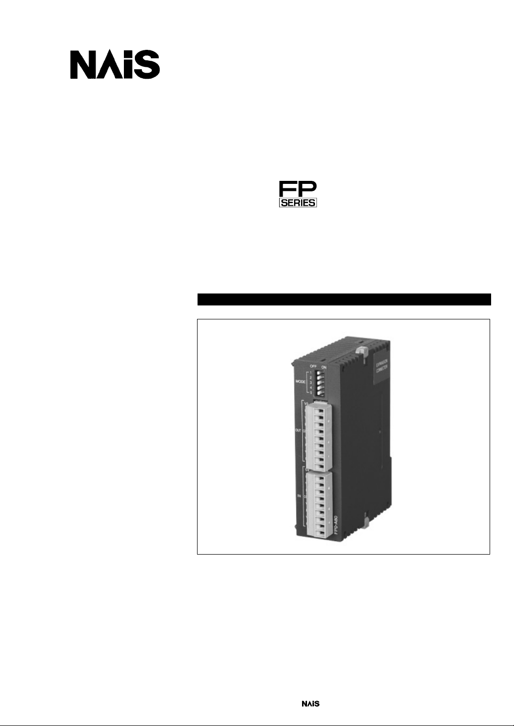
PROGRAMMABLE CONTROLLER
FP0
A/D Converter U nit
Technical Manual
is a global brand name of Matsushita Electric Works.
Page 2

BEFORE BEGINNING
This manual and everything described in it are copyrighted. You may not copy this
manual, in whole or part, without written consent of Matsushita Electric Works, Ltd.
Matsushita Electric Works, Ltd. pursues a policy of continuous improvement of the
design and performance of its products, therefore, we reserve the right to change the
manual/product without notice. In no event will Matsushita Electric Works, Ltd. be
liable for direct, special, incidental, or consequential damage resulting from any
defect in the product or its documentation, even if advised of the possibility of such
damages.
LIMITED WARRANTY
If physical defects caused by distribution are found, Matsushita Electric Works, Ltd.,
will replace/repair the product free of charge. Exceptions include:
D When physical defects are due to different usage/treatment of the
product other than described in the manual.
D When physical defects are due to defective equipment other than the
distributed product.
D When physical defects are due to modifications/repairs by someone
other than Matsushita Electric Works, Ltd.
D When physical defects are due to natural disasters.
MS-DOS and Windows are registered trademarks of Microsoft Corporation.
IBM Personal Computer AT is a registered trademark of the International Business
Machines Corporation.
Page 3

Table of Contents
Chapter 1 Parts and Terminology
1.1 Parts and Functions 1-2. . . . . . . . . . . . . . . . . . . . . . . . . . . . . . . . . . . . . . . . . . . .
1.2 Analog Input Terminal Block 1-3. . . . . . . . . . . . . . . . . . . . . . . . . . . . . . . . . . . . .
1.3 Expansion Limit 1-4. . . . . . . . . . . . . . . . . . . . . . . . . . . . . . . . . . . . . . . . . . . . . . . .
Chapter 2 Wiring and Input Range Setting Switch
2.1 Wiring 2-2. . . . . . . . . . . . . . . . . . . . . . . . . . . . . . . . . . . . . . . . . . . . . . . . . . . . . . . .
2.2 Input Range Setting (DIP) Switches 2-3. . . . . . . . . . . . . . . . . . . . . . . . . . . . . .
Chapter 3 A/D Conversion Characteristics
3.1 Current Range 3-2. . . . . . . . . . . . . . . . . . . . . . . . . . . . . . . . . . . . . . . . . . . . . . . . .
3.2 Voltage Range 3-3. . . . . . . . . . . . . . . . . . . . . . . . . . . . . . . . . . . . . . . . . . . . . . . . .
3.3 Averaging Function for Voltage and Current Ranges 3-6. . . . . . . . . . . . . . . .
Chapter 4 I/O Allocation and Program
4.1 I/O Number of A/D Converter Unit 4-2. . . . . . . . . . . . . . . . . . . . . . . . . . . . . . . .
4.2 Program of A/D Converter Unit 4-4. . . . . . . . . . . . . . . . . . . . . . . . . . . . . . . . . .
Chapter 5 Specifications and Dimensions
5.1 Specifications 5-2. . . . . . . . . . . . . . . . . . . . . . . . . . . . . . . . . . . . . . . . . . . . . . . . .
5.2 Dimensions 5-5. . . . . . . . . . . . . . . . . . . . . . . . . . . . . . . . . . . . . . . . . . . . . . . . . . .
Index
Record of Changes
Page 4

Table of Contents FP0 A/D Converter Unit
ii Matsushita Electric Works (Europe) AG
Page 5

Chapter 1
Parts and Terminology
Page 6
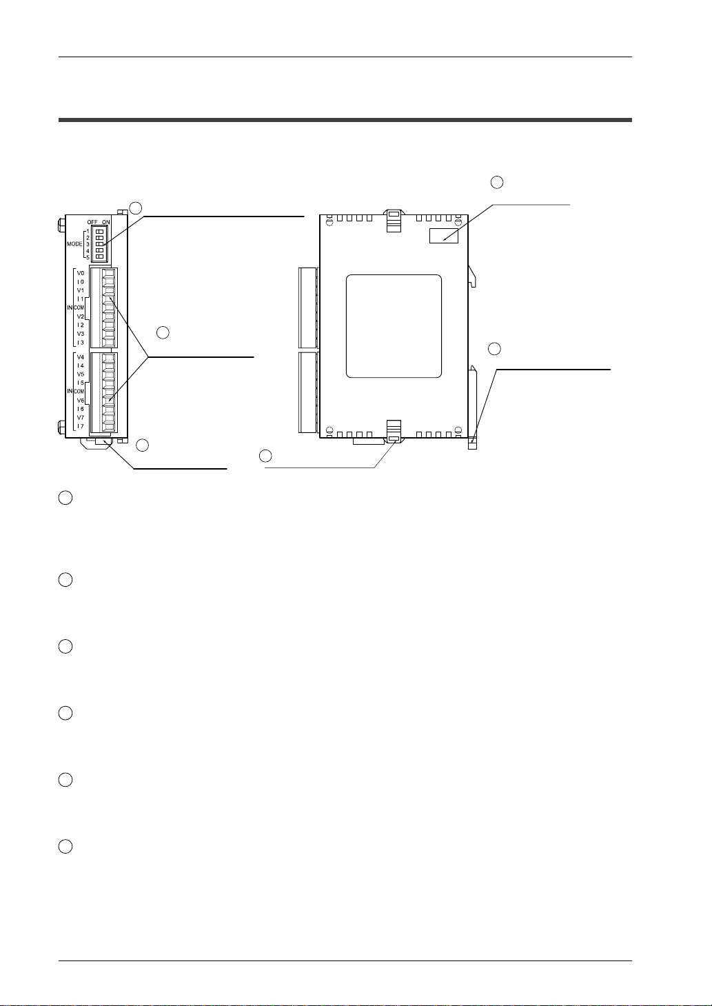
1.1 Parts and Functions
FP0–A80 A/D converter unit
1 Input range setting switches
2
Analog input
terminal block
FP0 A80
3
Power supply
connector
6
Expansion hook
FP0 A/D Converter UnitParts and Terminology
4
Expansion
connector
5
DIN rail attachment
lever
1
Input range setting (DIP) switches (voltage/current)
This switch is used to change the input mode (between voltage and current). All eight
input channels of the A/D converter unit operate at the same level. See page 2-3 for
details.
2
Analog input terminal block (9-pin)
Use a terminal block socket made by Phoenix Contact Co. (product number: 1840434).
(See FP0 Hardware Manual.)
3
Power supply connector
The power supply connector (supply 24V DC) is hooked up by using the power supply
cable (AFP0581) that comes with the unit.
4
Expansion connector
The expansion connector hooks up the expansion unit to the internal circuit of this unit.
(See FP0 Hardware Manual.)
5
DIN rail attachment lever
The DIN rail attachment lever allows simple attachment to a DIN rail. The lever is also
used for installation on a FP0 slim type mounting plate (AFP0803).
6
Expansion hook
The expansion hook is used to secure expansion units.
1-2
Matsushita Electric Works (Europe) AG
Page 7
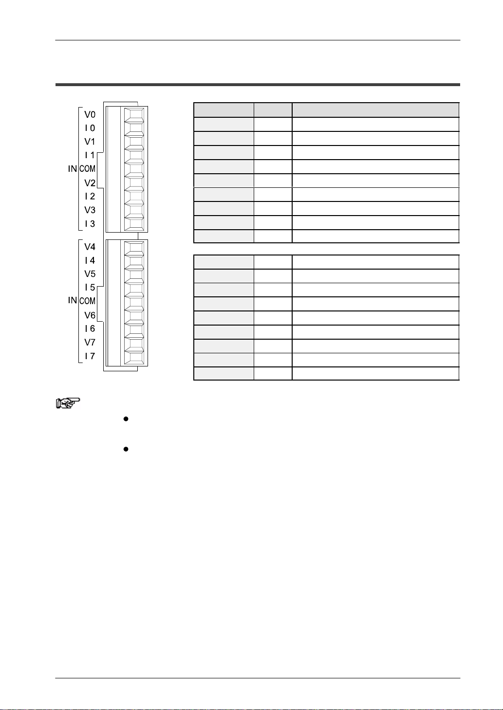
FP0 A/D Converter Unit 1.2 Analog Input Terminal Block
1.2 Analog Input Terminal Block
Pin number Name Description
1 V0 Analog input channel 0, voltage input
2 I0 Analog input channel 0, current input
3 V1 Analog input channel 1, voltage input
4 I1 Analog input channel 1, current input
5 COM Analog input, input common
6 V2 Analog input channel 2, voltage input
7 I2 Analog input channel 2, current input
8 V3 Analog input channel 3, voltage input
9 I3 Analog input channel 3, current input
1 V4 Analog input channel 4, voltage input
2 I4 Analog input channel 4, current input
3 V5 Analog input channel 5, voltage input
4 I5 Analog input channel 5, current input
5 COM Analog input, input common
6 V6 Analog input channel 6, voltage input
7 I6 Analog input channel 6, current input
8 V7 Analog input channel 7, voltage input
9 I7 Analog input channel 7, current input
Notes
When the analog input is a current signal, bridge the V and I
input pins externally.
The two COM terminals are connected internally.
1-3Matsushita Electric Works (Europe) AG
Page 8

FP0 A/D Converter UnitParts and Terminology
1.3 Expansion Limit
The unit can be connection to a combined maximum of three other expansion units and
intelligent units.
1-4
Matsushita Electric Works (Europe) AG
Page 9

Chapter 2
Wiring and Input Range Setting Switch
Page 10
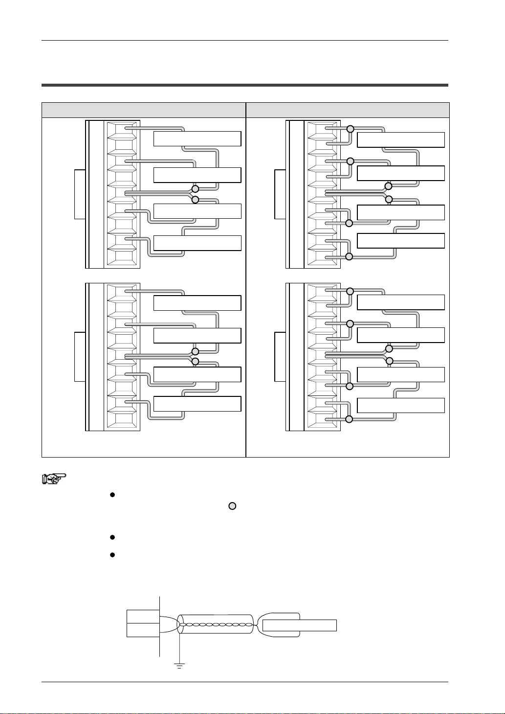
2.1 Wiring
Voltage input Current input
FP0 A/D Converter UnitWiring and Input Range Setting Switch
V0
I0
I0
V1
I1
COM
V2
I2
V3
I3
V4
I4
V5
I5
COM
V6
I6
V7
I7
Input instrument (ch0)
Input instrument (ch1)
Input instrument (ch2)
Input instrument (ch3)
Input instrument (ch4)
Input instrument (ch5)
Input instrument (ch6)
Input instrument (ch7)
V0
I0
V1
I1
COM
V2
I2
V3
I3
V4
I4
V5
I5
COM
V6
I6
V7
I7
Input instrument (ch0)
Input instrument (ch1)
Input instrument (ch2)
Input instrument (ch3)
Input instrument (ch4)
Input instrument (ch5)
Input instrument (ch6)
Input instrument (ch7)
Connect input instrument between V terminal and COM
terminal.
Notes
Tie the COM connectors for two channels together as indicated
by the gray circles (
than two wires go to each COM terminal.
The two COM terminals are connected internally.
We recommend that you use dual–core twisted pair shielded
wiring for the analog input wiring, and that you connect the
shield to earth.
V
COM
2-2
First, connect both V terminal and I terminal. And then
connect input instrument between it and COM terminal.
) in the diagram above so that no more
Input instrument
Matsushita Electric Works (Europe) AG
Page 11
FP0 A/D Converter Unit 2.2 Input Range Setting (DIP) Switches
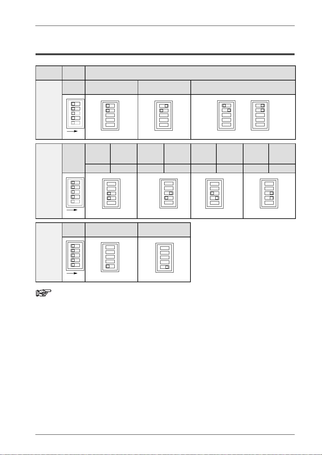
2.2 Input Range Setting (DIP) Switches
Mode Switch
Analog
input
range
Number
of input
channels
Averaging
function
number
1 and 2
1
2
ON
3 and 4
3
4
ON
5 No averaging
Range
0 to 5V 0 to 20mA
(see note 1)
Conversion
channel
ch0 and 1 2 ch0 to 3 4 ch0 to 5 6 ch0 to 7 8
Number
of input
channels
(see note 2)
–10 to 10V –100 to 100mV
Conversion
channel
With averaging
Number
of input
channels
(see note 3)
Conversion
channel
Number
of input
channels
or
Conversion
channel
Number
of input
channels
5
Notes
ON
1) It is possible to use the 0 to 5V range and 0 to 20mA range
together.
2) The A/D conversion data is set for the specified input contact
point area for each A/D conversion on each channel.
3) On each channel, for each A/D conversion, the maximum and
minimum values from the data of the last ten times are
excluded, and the data from the other eight times is averaged,
and the result set.
(Use when the environment contains a lot of noise.)
4) The switch reads only once when the power supply of FP0
control unit is turned on.
2-3Matsushita Electric Works (Europe) AG
Page 12

FP0 A/D Converter UnitWiring and Input Range Setting Switch
2-4
Matsushita Electric Works (Europe) AG
Page 13

Chapter 3
A/D Conversion Characteristics
Page 14
3.1 Current Range
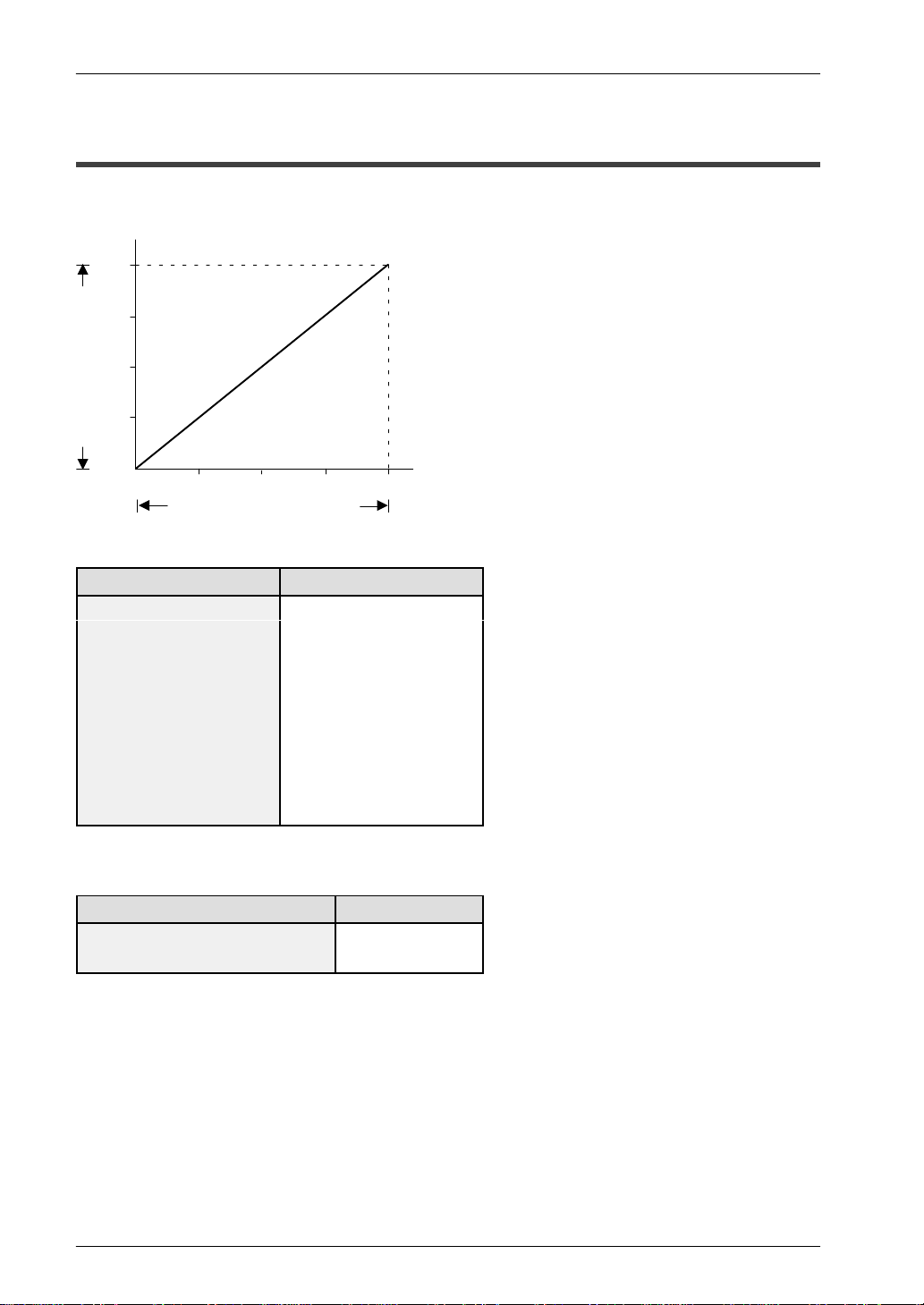
Current range: 0 to 20mA DC input
(K)
4000
3000
2000
1000
A/D conversion value
FP0 A/D Converter UnitA/D Conversion Characteristics
0
5 10 15 20(mA)
Analog input range
Corresponding table of A/D conversion values
Input current (mA) A/D conversion value
0.0 0
2.5 500
5.0 1000
7.5 1500
10.0 2000
12.5 2500
15.0 3000
17.5 3500
20.0 4000
Processing if the range is exceeded
Input value Converted value
0mA or less (including negative value) 0
20mA or more 4000
3-2
Matsushita Electric Works (Europe) AG
Page 15
FP0 A/D Converter Unit 3.2 Voltage Range
3.2 Voltage Range
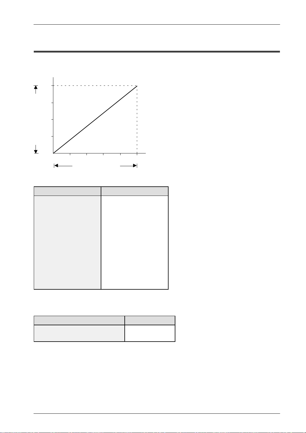
Voltage range: 0 to 5V DC input
(K)
4000
3000
2000
1000
A/D conversion value
0
1 2 3 4 5(V)
Analog input range
Corresponding table of A/D conversion values
Input voltage (V) A/D conversion value
0.0 0
0.5 400
1.0 800
1.5 1200
2.0 1600
2.5 2000
3.0 2400
3.5 2800
4.0 3200
4.5 3600
5.0 4000
Processing if the range is exceeded
Input value Converted value
0V or less (including negative value) 0
5V or more 4000
3-3Matsushita Electric Works (Europe) AG
Page 16
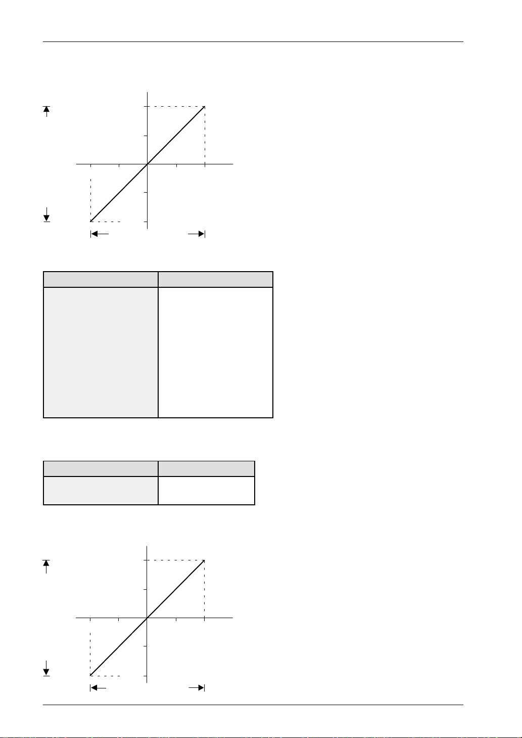
Voltage range: –10 to +10V DC input
(K)
2000
1000
0
–10 –5 5 10 (V)
FP0 A/D Converter UnitA/D Conversion Characteristics
A/D conversion value
–1000
–2000
Analog input range
Corresponding table of A/D conversion values
Input voltage (V) A/D conversion value
–10.0 –2000
–7.5 –1500
–5.0 –1000
–2.5 –500
0.0 0
+2.5 +500
+5.0 +1000
+7.5 +1500
+10.0 +2000
Processing if the range is exceeded
Input value Converted value
–10V or less –2000
+10V or more +2000
Voltage range: –100 to +100mV DC input
(K)
2000
1000
0
–100
A/D conversion value
3-4
–50 50 100 (mV)
–1000
–2000
Analog input range
Matsushita Electric Works (Europe) AG
Page 17
FP0 A/D Converter Unit 3.2 Voltage Range
Corresponding table of A/D conversion values
Input voltage (mV) A/D conversion value
–100.0 –2000
–75.0 –1500
–50.0 –1000
–25.0 –500
0.0 0
+25.0 +500
+50.0 +1000
+75.0 +1500
+100.0 +2000
Processing if the range is exceeded
Input value Converted value
–100mV or less –2000
+100mV or more +2000
3-5Matsushita Electric Works (Europe) AG
Page 18
FP0 A/D Converter UnitA/D Conversion Characteristics
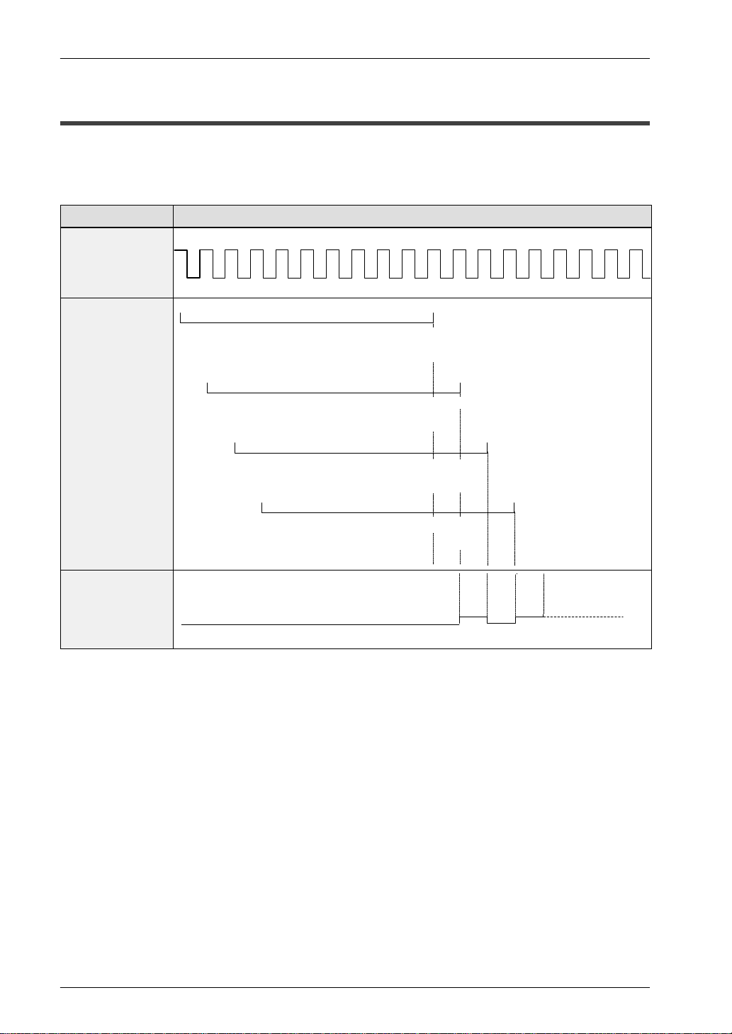
3.3 Averaging Function for Voltage and Current Ranges
When the averaging function is set to on, the internal processing of the A/D conversion
unit is as shown in the diagram below (in this example there are two input channels, and
the input range setting switch Nos. 3 and 4 are off).
Operation item Time chart
1ms
1ms
Analog input
value for ch0
(Reading time)
Internal processing for A/D conversion unit ch0
ch0
1800 1780 1820 1790 1800 1850 1900 1830 1870
1ms
ch1
ch1
ch1
ch1
ch1
ch1
ch1
ch1
ch1
ch1
ch0
ch0
ch0
ch0
ch0
ch0
ch0
ch0
ch0
ch0
1800
1780 1820 1790 1800 1850 1900 1830 1870 1910 1780 1810 1950
Averaging of results from 8 times, with
max/min values deleted.
(1800+1820+1790+1800+1850+1900+1830+
1910
1870)
min
deleted deleted
1780 1820 1790 1800 1850 1900 1830 1870
min
deleted
1820 1790 1800 1850 1900 1830 1870
1790 1800 1850 1900 1830 1870
max
1910
max
deleted
1910
max min
deleted
1910
1780
1780
deleted
1780
min
deleted
ch1
ch1
ch1
ch1
ch1
ch0
ch0
ch0
ch0
ch0
8=1832.50
→
(1820+1790+1800+1850+1900+1830+
1870+1780)
1810
1810 1950
8=1830.00
→
(1820+1790+1800+1850+1900+
1830+1870+1810) → 8=1833.75
(1790+1800+1850+1900+
1830+1870+1910+1810)
=1845
max
deleted
ch1
ch0
ch1
ch0
ch1
8
→
Digital output
value for ch0
K1832
K1833 K1845
K1830
Starting with the most recent data, the data from the last ten times is taken. The
maximum and minimum values are deleted, and the averaging is carried out on the
remaining eight items. The obtained values are output to WX2 and WX3. The values
output at this time always use the most recent averaged value (decimals are discarded).
3-6
Matsushita Electric Works (Europe) AG
Page 19

Chapter 4
I/O Allocation and Program
Page 20
4.1 I/O Number of A/D Converter Unit
I/O number of A/D converter unit
FP0 A/D Converter UnitI/O Allocation and Program
FP0 Control unit
First
expansion
WX2
WX3
WY2
WY3
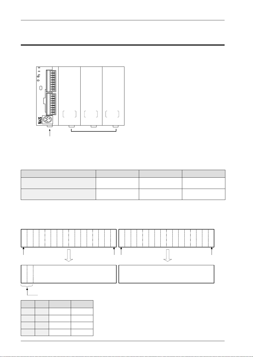
A combined maximum of three A/D converter
units and other expansion units can be connected to one control unit. WX and WY are
allocated two words each (2 x 16 bits each).
Second
expansion
WX4
WX5
WY4
WY5
Third
expansion
WX6
WX7
WY6
WY7
With the setup illustrated in the diagram above, the data for each channel is allocated
as I/O data as indicated in the table below.
A/D converter unit input channel First expansion Second expansion Third expansion
ch0, 2, 4, 6
(Each 16 points)
ch1, 3, 5, 7
(Each 16 points)
WX2
(X20 to X2F)
WX3
(X30 to X3F)
WX4
(X40 to X4F)
WX5
(X50 to X5F)
WX6
(X60 to X6F)
WX7
(X70 to X7F)
Example of I/O allocation
The diagram below shows you the allocation of each channel’s conversion data, WX2
and WX3 when this unit is connected to the first expansion.
X
X
X
X
X
X
X
X
X
3
3
3
3
3
3
3
3
3
F
E
D
C
B
A
9
8
7
Bit F
A1A
0
Conversion data of ch1, 3, 5, 7
(14 bit with sign)
Conversion data switch flag
A1 A0 WX3 WX2
0 0 ch1 data ch0 data
0 1 ch3 data ch2 data
1 0 ch5 data ch4 data
1 1 ch7 data ch6 data
4-2
X
X
X
X
X
X
X
X
X
X
X
X
X
X
X
X
X
X
X
X
X
X
X
3
3
3
3
3
3
3
2
2
2
2
2
2
2
2
2
2
2
2
2
2
2
2
6
5
4
3
2
1
0
F
E
D
C
B
A
9
8
7
6
5
4
3
2
1
0
Bit 0
Bit F
Conversion data of ch0, 2, 4, 6
(16 bit with sign)
Bit 0
Matsushita Electric Works (Europe) AG
Page 21
FP0 A/D Converter Unit 4.1 I/O Number of A/D Converter Unit
Conversion data switch flags
The resolution of the A/D converter unit is 12 bits, but when data is transferred to the
control unit, it is converted to 16–bit data. Therefore, although the WX2 data requires no
processing, for the WX3 data, the top two bits are used as conversion data switching
flags. Accordingly, the top two bits are processed as follows.
When the A/D conversion data is negative “–”, the WX2 and WX3 data become two’s
complement.
In other words, bit C to bit F of WX2 and bit C to bit D of WX3 become “1”.
Also, because the top two bits of WX3 are used as conversion data switch flags, masking
is required so that the bits are “00” when the conversion data is positive “+”, and “11”
when the conversion data is negative “–”.
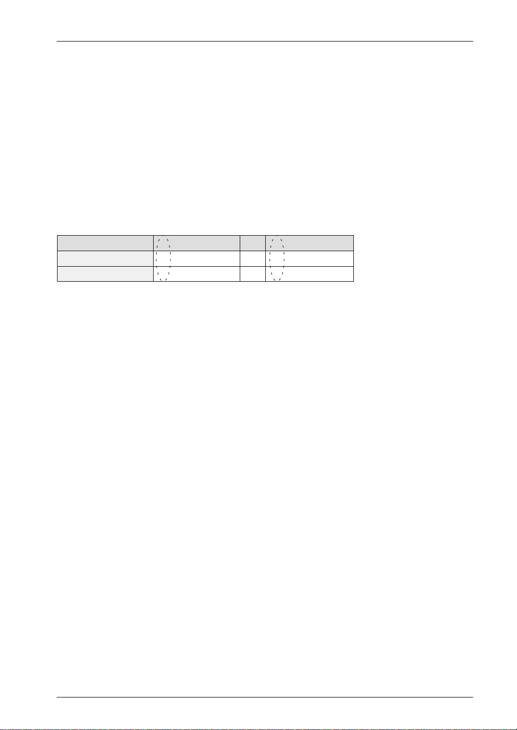
Ch3 data WX3 → Data after masking
1 0100000000000001
–1 0111111111111111
Conversion data switch flags Mask applied to the above values
0000000000000001
→
1111111111111111
→
4-3Matsushita Electric Works (Europe) AG
Page 22
FP0 A/D Converter UnitI/O Allocation and Program
4.2 Program of A/D Converter Unit
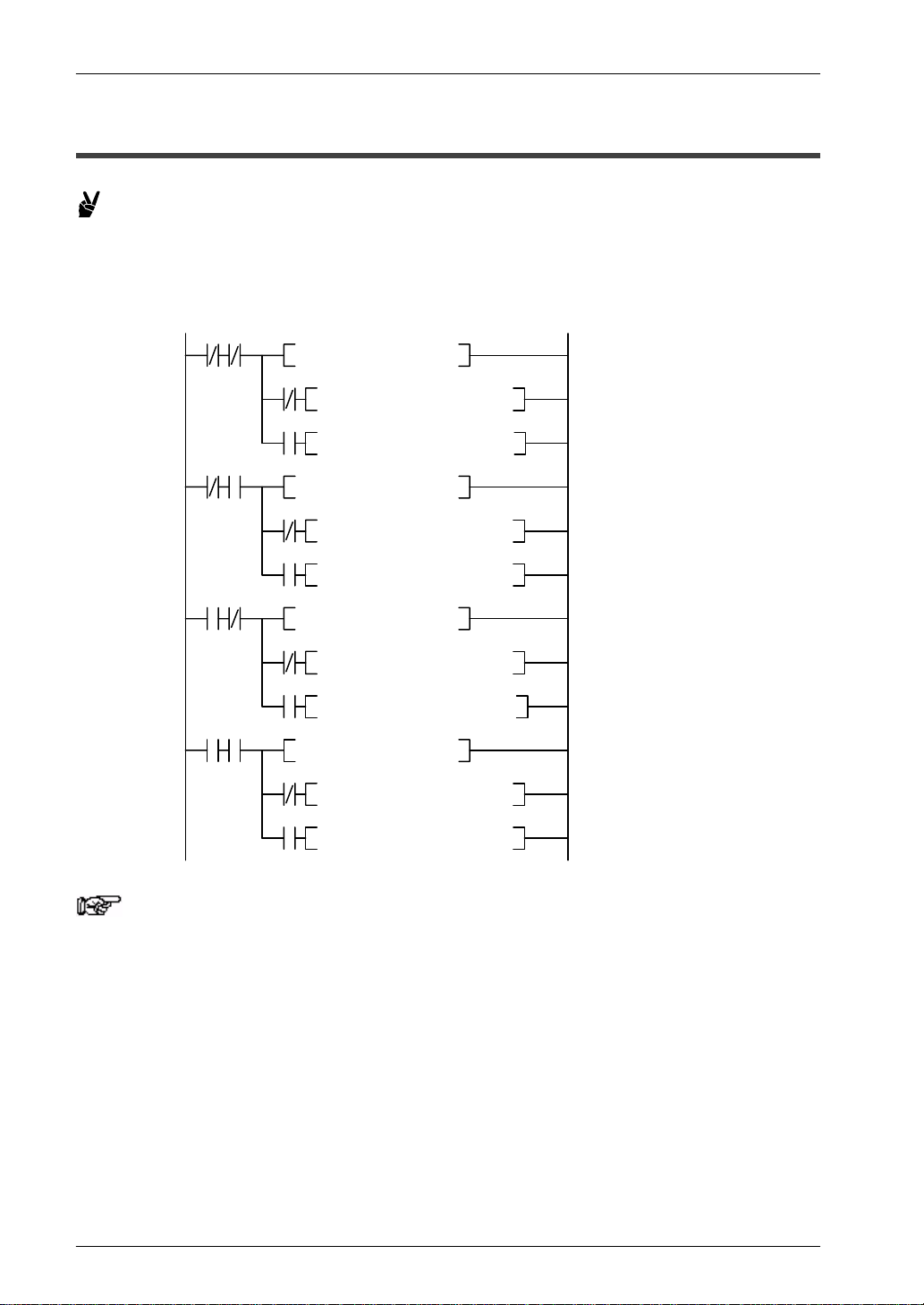
Programming example for FPWIN–GR
Ladder program example for loading data from each channel
Indicates the program that stores in data registers DT0 to DT7 the from ch0 to
ch7 A/D conversion data that is assigned to the first expansion.
X3FX3E
Load ch0 and
ch1 data
X3FX3E
Load ch2 and
ch3 data
X3FX3E
Load ch4 and
ch5 data
X3FX3E
Load ch6 and
ch7 data
F0 MV WX2, DT0
X3D
F65 WAN WX3, H FFF, DT1
X3D
F66 WOR HC000,
F0 MV WX2, DT2
X3D
F65 WAN WX3, H FFF, DT3
X3D
F66 WOR WX3, HC000,DT3
F0 MV WX2, DT4
X3D
F65 WAN WX3, H FFF, DT5
X3D
F66 WOR WX3, HC000,DT5
F0 MV WX2, DT6
X3D
F65 WAN WX3, H FFF, DT7
X3D
F66 WOR WX3, HC000, DT7
ch0 data –> DT0
When ch1 data is positive –> DT1
DT1WX3,
When ch1 data is negative –> DT1
ch2 data –> DT2
When ch3 data is positive –> DT3
When ch3 data is negative –> DT3
ch4 data –> DT4
When ch5 data is positive –> DT5
When ch5 data is negative –> DT5
ch6 data –> DT6
When ch7 data is positive –> DT7
When ch7 data is negative –> DT7
4-4
Note
If the expansion positions have changed, see page 4-2 and
change X3D, X3E, X3F, WX2 and WX3.
Matsushita Electric Works (Europe) AG
Page 23
FP0 A/D Converter Unit 4.2 Program of A/D Converter Unit
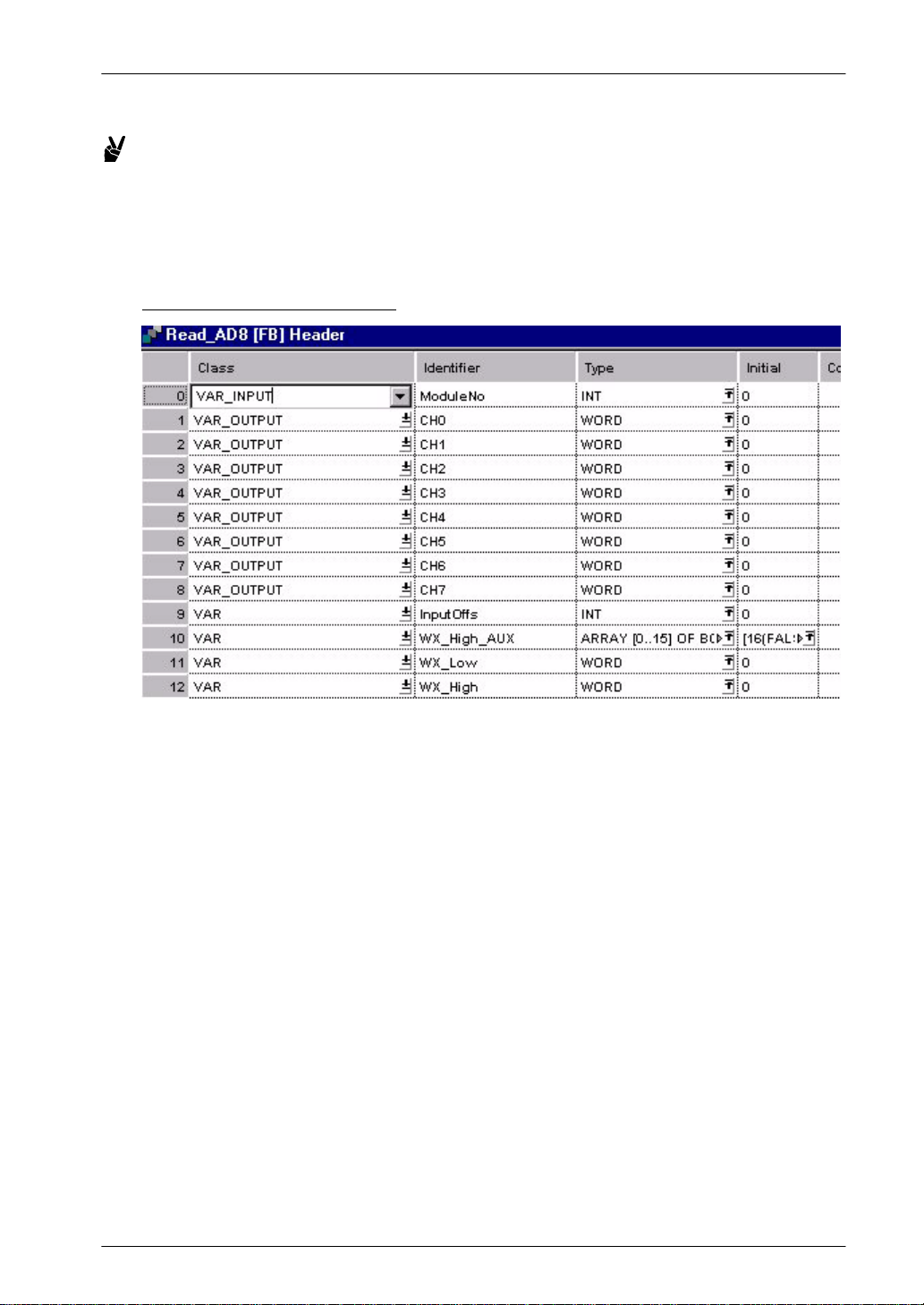
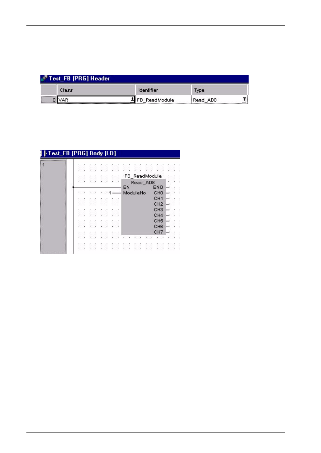
Programming example for Control FPWIN Pro
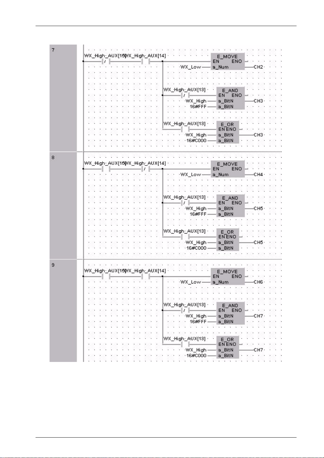
The following FPWIN Pro function block reads all 8 analog inputs of the FP0
AD8 unit and stores the result in 16–bit words.
The following example consists of the function block and the programming
example.
Header of the Function Block
4-5Matsushita Electric Works (Europe) AG
Page 24
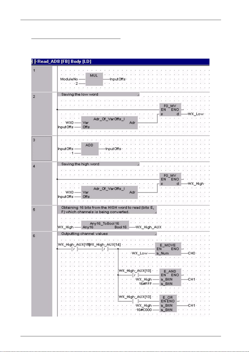
Ladder Diagram of the Function Block
FP0 A/D Converter UnitI/O Allocation and Program
4-6
Matsushita Electric Works (Europe) AG
Page 25
FP0 A/D Converter Unit 4.2 Program of A/D Converter Unit
4-7Matsushita Electric Works (Europe) AG
Page 26
FP0 A/D Converter UnitI/O Allocation and Program
POU Header
All input and output variables that are required for the program are declared in
the POU header.
Ladder Diagram Body
This example was created with the programming editor Ladder Diagram. In
Control FPWIN Pro, you can also write the program in Instruction List, Function
Block Diagram, or Sequential Function Chart.
4-8
Matsushita Electric Works (Europe) AG
Page 27

Chapter 5
Specifications and Dimensions
Page 28
FP0 A/D Converter UnitSpecifications and Dimensions
5.1 Specifications
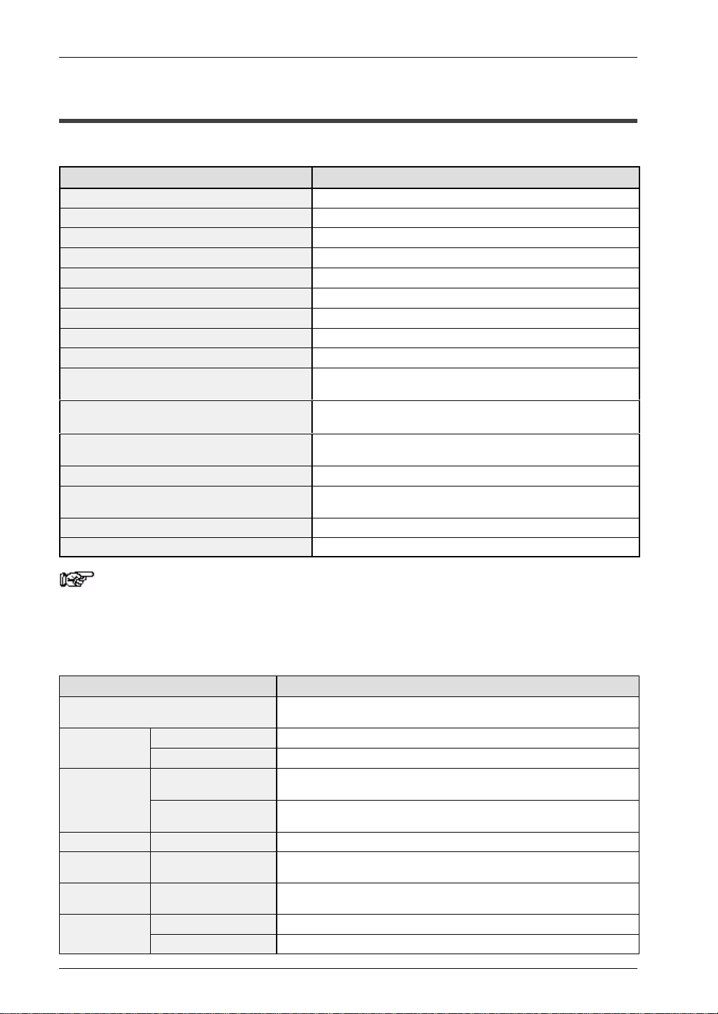
General specifications
Item Description
Rated operation voltage 24V DC
Operating voltage range 21.6 to 26.4V DC
Rated current consumption 60mA or less (at 24V DC)
Current consumption increase of control unit 20mA or less (at 24V DC) (see note)
Allowable instantaneous stop time 10ms
Ambient temperature 0 to +55°C/32 to + 131°F
Storage temperature –20 to +70°C/–4 to +158°F
Ambient humidity 30 to 85%RH (non–condensing)
Storage humidity 30 to 85%RH (non–condensing)
Breakdown voltage
Insulation resistance
Vibration resistance
Shock resistance Shock of 98m/s2 or more, 4 times on 3 axes
Noise immunity
Operating condition Free from corrosive gases and excessive dust
Weight Approx. 90g/3.175oz
500V AC for 1 minute between analog input terminal and power
supply/ground terminal
Min. 100MΩ (measured with a 500V DC megger) for between
analog input terminal and power supply/ground terminal
10 to 55Hz, 1 cycle/min: double amplitude of 0.75mm/ 0.030in.,
10 min on 3 axes
1,000 Vp-p with pulse widths 50ns and 1µs (based on in-house
measurements)
Note
For each additional A/D converter unit connected to a control
unit, the current consumption increases by 20mA (max.).
Analog input specifications
Item Description
Number of input points
Input range
Digital output
Resolution Voltage/Current range 1/4000 (12bits)
Conversion
speed
Overall preci-
sion
Input imped-
Input impedance
Voltage range 0 to 5V, –10 to +10V, –100 to +100mV
Current range 0 to 20mA
0 to 5V
0 to 20mA
–10 to +10V
–100 to 100mV
Voltage/Current range 1ms/channel (see note 2)
Voltage/Current range
Voltage range 1 MΩ or more
Current range 250Ω
8 channels/unit (the number of input points can be switched to 2, 4, 6 or
8 channels)
K0 to K4000 (H0000 to H0FA0, see note 1)
K –2000 to K +2000 (HF830 to H07D0 , see note 1)
±1%F.S. or less (at 0 to 55°C/32 to 131°F), ±0.6% F.S. or less
(at 25°C/77°F)
5-2
Matsushita Electric Works (Europe) AG
Page 29
FP0 A/D Converter Unit 5.1 Specifications
DescriptionItem
Absolute max-
Absolute maximum input
Insulation method (see note 3)
Number of FP0 input contact points
Averaging function Can be switched on and off
Voltage range ±15V
Current range +30mA
Between analog input terminal to FP0 internal circuit:
photocoupler insulation (non-insulated between analog inputs)
Between analog input terminal to A/D converter unit external power supply:
insulation-type DC/DC converter
32 input contact points
First half (16 points): analog input ch0, 2, 4 and 6 data (WX2)
(see note 4)
Second half (16 points): analog input ch1, 3, 5 and 7 data (WX3)
(see note 4)
32 output contact points (Not used)
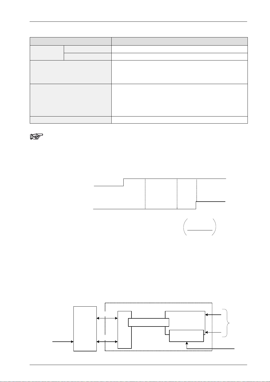
Notes
1) If the analog input value exceeds the upper/lower limit, the
digital value is held at the upper/lower limit.
2) The time noted below is required before the analog data is
reflected in the control unit input.
10V
Analog input
WX2
0V
K0
Conversion
time
Conversion time: 1ms to 1ms x number of input channels
Refresh standby time: 0ms to scan time x
Refresh time: 1ms x number of expansion units
Refresh
standby time
Refresh
time
number of
input channels
K2000
2
Set switch for the number of input channels.
The control unit loads two channels worth of data at each
control unit scan. In other words, if the switch for the number
of input channels is set to eight channels, the control unit data
is updated once every four scans.
3) Refer to the schematic diagram of insulation methods below.
A/D converter unit
Bus
Analog input circuit
DC/DC
converter insulation
24V DC
FP0
control unit
Photocoupler insulation
I/F
+5V
ch0 to ch7
24V DC
5-3Matsushita Electric Works (Europe) AG
Page 30

FP0 A/D Converter UnitSpecifications and Dimensions
4) The contact numbers change depending on the expansion
position. (These values represent when the unit is installed in
the closest position to the control unit.) For details,
see page 4-2.
5-4
Matsushita Electric Works (Europe) AG
Page 31
FP0 A/D Converter Unit 5.2 Dimensions
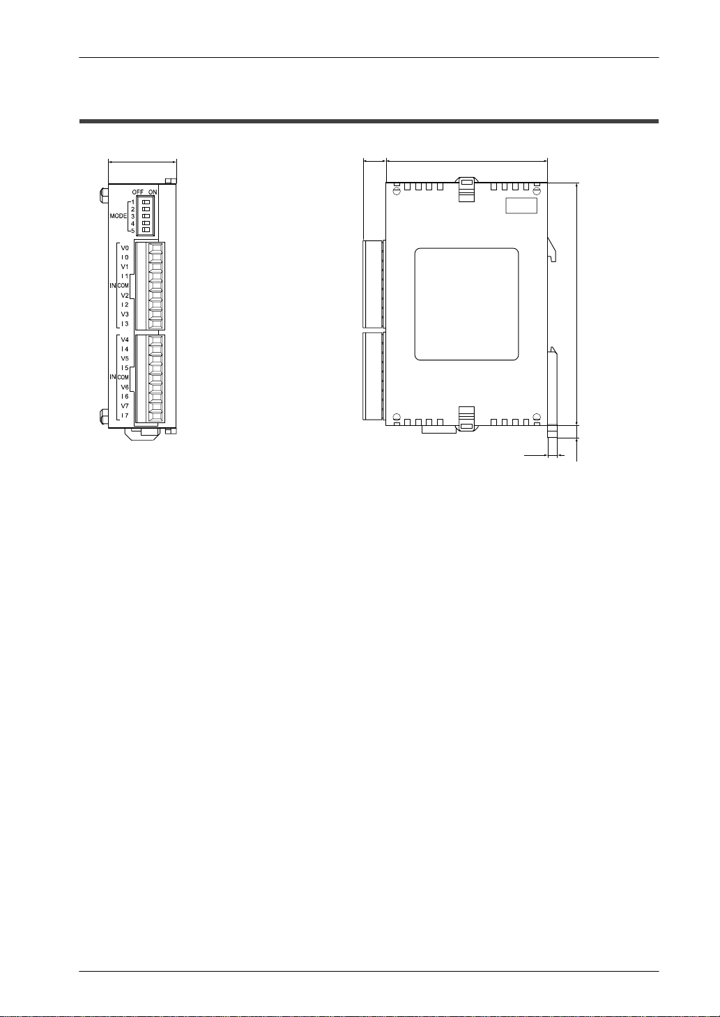
5.2 Dimensions
25.0/0.984
FP–A80
60.0/2.36210.0/0.394
3.5/0.138
90.0/3.543
4.5/0.177
(unit: mm/in.)
5-5Matsushita Electric Works (Europe) AG
Page 32

FP0 A/D Converter UnitSpecifications and Dimensions
5-6
Matsushita Electric Works (Europe) AG
Page 33

Index
A
A/D Conversion Characteristics, 3 - 2
Averaging Function, 3 - 6
Current Range, 3 - 2
Voltage Range, 3 - 3
Analog Input Terminal Block, 1 - 2, 1 - 3
D
Dimensions, 5 - 5
DIN Rail Attachment Lever , 1 - 2
DIP Switches. See Input Range Setting
Switches
E
Expansion Connector, 1 - 2
Expansion Hook, 1 - 2
Expansion Limit, 1 - 4
P
Parts, 1 - 2
Power Supply Connector, 1 - 2
S
Specifications, 5 - 2
Analog Input, 5 - 2
General, 5 - 2
W
Wiring, 2 - 2
F
Functions, 1 - 2
I
I/O Allocation, 4 - 2
Conversion Data Switch Flags, 4 - 3
I/O Number, 4 - 2
Program, 4 - 4
Input Instrument, 2 - 2
Input Range Setting Switch
Conversion Channel, 2 - 3
Number of Input Channels, 2 - 3
Input Range Setting Switches, 1 - 2, 2 - 3
Page 34

Index FP0 A/D Converter Unit
I-2
Matsushita Electric Works (Europe) AG
Page 35

Record of Changes
Manual No. Date Description of changes
ARCT1F321END JUNE 2001 First European Edition
Page 36

GLOBAL NETWORK
North America Europe Asia Pacific China Japan
Aromat
Corporation
Matsushita
Electric Works Group
Europe
H Austria Matsushita Electric Works Austria GmbH
H Benelux Matsushita Electric Works Benelux B. V.
H France Matsushita Electric Works France S.A.R.L.
H Germany Matsushita Electric Works Deutschland GmbH
H Ireland Matsushita Electric Works Ltd., Irish Branch Office
H Italy Matsushita Electric Works Italia s.r.l.
H Portugal Matsushita Electric Works Portugal, Portuguese Branch Office
H Scandinavia Matsushita Electric Works Scandinavia AB
H Spain Matsushita Electric Works España S.A.
H Switzerland Matsushita Electric Works Schweiz AG
H United Kingdom Matsushita Electric Works UK Ltd.
Stojanstraße 12, 2344 Maria Enzersdorf, Austria, Tel. (02236) 2 68 46, Fax (02236) 46133, http://www.matsushita.at
De Rijn 4, (Postbus 211), 5684 PJ Best, (5680 AE Best), Netherlands, Tel. (0499) 37 2727, Fax (0499) 372185, http://www.matsushita.nl
B.P. 44, 91371 Verrières le Buisson CEDEX, France, Tel. 01 60 13 57 57, Fax 01 60 13 57 58, http://www.matsushita–france.fr
Rudolf–Diesel–Ring 2, 83607 Holzkirchen, Germany, Tel. (08024) 648–0, Fax (08024) 648–555, http://www.matsushita.de
Waverley, Old Naas Road, Bluebell, Dublin 12, Republic of Ireland, Tel. (01) 460 09 69, Fax (01) 460 11 31
Via del Commercio 3–5 (Z.I. Ferlina), 37012 Bussolengo (VR), Italy, Tel. (045) 675 27 11, Fax (045) 670 04 44, http://www.matsushita.it
Avda 25 de Abril, Edificio Alvorada 5º E, 2750 Cascais, Portugal, Tel. (351) 1482 82 66, Fax (351) 1482 74 21
Sjöängsvägen 10, 19272 Sollentuna, Sweden, Tel. +46 8 59 47 66 80, Fax (+46) 8 59 47 66 90, http://www.mac–europe.com
Parque Empresarial Barajas, San Severo, 20, 28042 Madrid, Spain, Tel. (91) 329 38 75, Fax (91) 329 29 76
Grundstrasse 8, 6343 Rotkreuz, Switzerland, Tel. (041) 799 70 50, Fax (041) 799 70 55, http://www.matsushita.ch
Sunrise Parkway, Linford Wood East, Milton Keynes, MK14 6LF, England, Tel. (01908) 231 555, Fax (01908) 231 599,
http://www.matsushita.co.uk
Matsushita
Electric Works
(Asia Pacific)
Matsushita
Electric Works
Matsushita
Electric Works Ltd.
Automation Controls
Group
North & South America
H USA Aromat Corporation Head Office USA
629 Central Avenue, New Providence, N.J. 07974, USA, Tel. 1–908–464–3550, Fax 1–908–464–8513, http://www.aromat.com
Asia
H China Matsushita Electric Works, Ltd. China Office
H Hong Kong Matsushita Electric Works Ltd. Hong Kong
H Japan Matsushita Electric Works Ltd. Automation Controls Group
H Singapore Matsushita Electric Works Pte. Ltd. (Asia Pacific)
COPYRIGHT E 2001 All Rights Reserved ARCT1F0000ABC V1.x 12/99
Specifications are subject to change without notice. Printed in Europe
2013, Beijing Fortune, Building 5, Dong San Huan Bei Lu, Chaoyang Distric t, Beijing, China, Tel. 86–10–6590–8646, Fax 86–10–6590–8647
Rm1601, 16/F, Tower 2, The Gateway, 25 Canton Road, Tsimshatsui, Kowloon, Hong Kong, Tel. (852) 2956–3118, Fax (852) 2956–0398
1048 Kadoma, Kadoma–shi, Osaka 571–8686, Japan, Tel. 06–6908–1050, Fax 06–6908–5781, http://www.mew.co.jp/e–acg/
101 Thomson Road, #25–03/05, United Square, Singapore 307591,Tel. (65) 255–5473, Fax (65) 253–5689
ARCT1F321END V1.0 June 2001
 Loading...