

Ex. DSP
1
L DC12V R
Contact arrangement
1: 1a1b
1a: 1a
2a: 2a
Operating function
Nil: Single side stable
L2: 2 coil latching
Coil voltage
DC: 3, 5, 6,
9, 12, 24 V
Polarity
Nil: Standard polarity
R: Reverse polarity
(Note) Standard packing–Carton: 50 pcs.; Case: 500 pcs.
UL/CSA, VDE approved type is standard.
5 ×
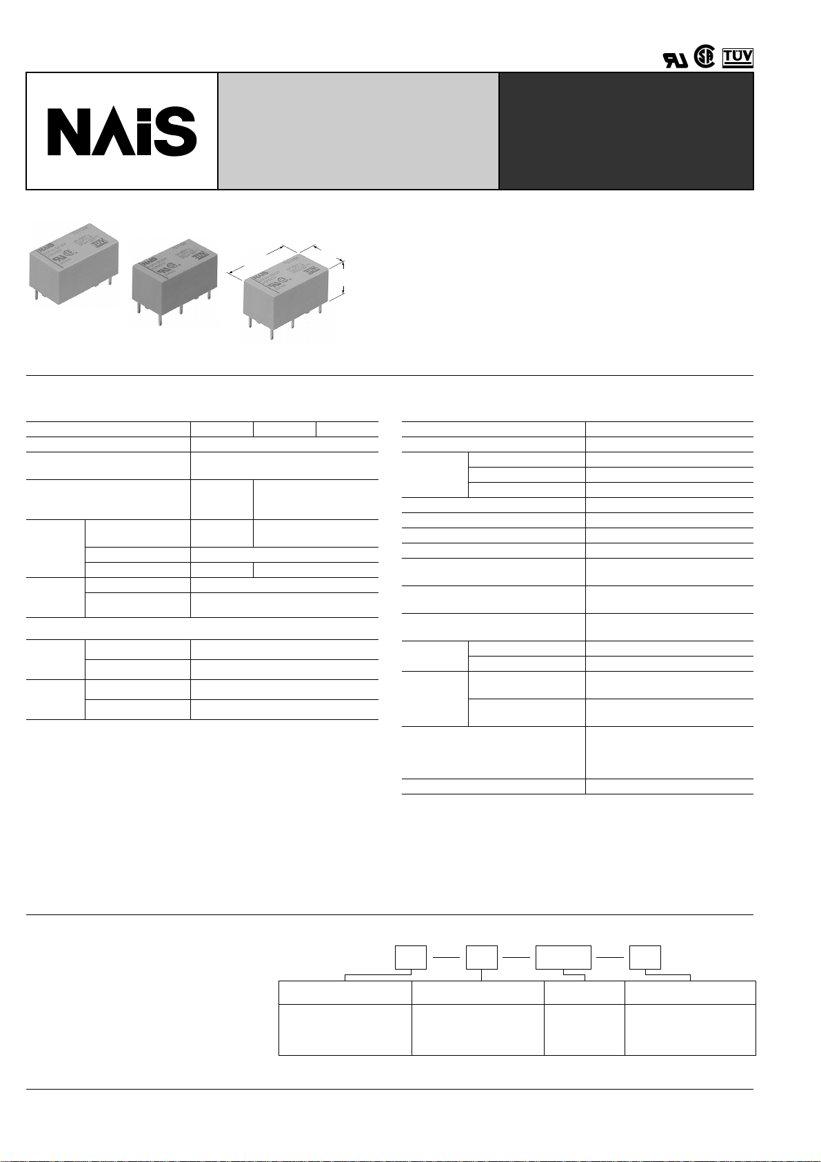
MINIA TURE PO WER RELAY
IN DS RELAY SERIES
11.0
.433
10.5
.413
DSP1a
DSP1
mm inch
20.2
.795
DSP2a
SPECIFICATIONS
Contact
Arrangement 1a 1a1b 2a
Contact material Gold flash over silver alloy
Initial contact resistance, max.
(By voltage drop 6 V DC 1A)
8A 250
Nominal switching capacity
VAC
5A 30 VDC
2,000 VA
150 W
8 A 5 A
Rating
(resistive)
Expected
life (min.
operations)
Max. switching power
Max. switching voltage
Max. switching current
Mechanical (at 180 cpm)
Electrical 10
Coil (polarized) (at 20 ° C 68 ° F)
Minimum
operating
power
Nominal
operating
power
Note: All specifications are based on the condition of 25 ° C 77°F, 50% R.H. unless
otherwise specified.
Single side stable 192 mW
2 coil latching 192 mW
Single side stable 300 mW
2 coil latching 300 mW
30 m Ω
5A 250 VAC
5A 30 VDC
1,250 VA
150 W
250 V AC, 30 V DC
7
10
5
DSPRELAYS
FEATURES
• Power types added to DS relay series
• High switching capacity: 1a: 8 A 250 V AC / 1a1b, 2a: 5 A 250 V AC
• High sensitivity: 190 mW pick-up power
• High contact welding resistance
• Latching types available
• High breakdown voltage 3,000 Vrms between contacts and coil
1,000 Vrms between open contacts Meeting FCC Part 68
• Sealed types are standard
Characteristics
Max. operating speed 30 cps. at rated load
Initial insulation resistance*
Initial
breakdown
voltage*
Between open contacts
Between contact sets 2,000 Vrms (1a1b, 2a)
2
Between contacts and coil
Surge voltage between contacts and coil
Set time*
Reset time*
Operate time*
3
(at nominal voltage) Max. 10 ms (Approx. 5 ms)
3
(at nominal voltage) Max. 10 ms (Approx. 4 ms)
3
(at nominal voltage) Max. 10 ms (Approx. 5 ms)
Release time(without diode)*
(at nominal voltage)
Temperature rise
Soldering temperature
Shock
resistance
Vibration
resistance
Conditions for operation, transport
and storage*
Functional*
Destructive*
Functional*
Destructive
7
(Not freezing and condensing at low
temperature)
Unit weight Approx. 4.3 g .15 oz
Remarks
* Specifications will vary with foreign standards certification ratings.
1
Measurement at same location as "Initial breakdown voltage" section
*
2
*
Detection current: 10mA
3
*
Excluding contact bounce time
4
Half-wave pulse of sine wave: 11ms; detection time: 10 µ s
*
5
*
Half-wave pulse of sine wave: 6ms
6
Detection time: 10 µ s
*
7
R
*
efer to 5. Conditions for operation, transport and storage mentioned in
AMBIENT ENVIRONMENT (Page 61).
1
Min. 1,000 M Ω at 500 V DC
1,000 Vrms
3,000 Vrms
Min. 5,000 V
3
Max. 5 ms (Approx. 4 ms)
Max. 40 ° C (1a1b type)
Max. 55 ° C (1a, 2a types)
250 ° C (10 s) 300 ° C (5 s),
350 ° C (3 s)
4
5
6
Min. 196 m/s
Min. 980 m/s
117.6 m/s
at double amplitude of 2 mm
205.8 m/s
2
{20 G}
2
{100 G}
2
{12 G}, 10 to 55 Hz
2
{21 G}, 10 to 55 Hz
at double amplitude of 3.5 mm
–40 ° C to +65 ° C – 40 ° F 149 ° F
TYPICAL APPLICATIONS
Office and industrial electronic devices
• Terminal devices of information processing equipment, such as printer, data recorder.
• Office equipment (copier, facsimile)
• Measuring instruments
• NC machines, temperature controllers
and programmable logic controllers.
234
ORDERING INFORMATION
8 1
+
–
16
5
6-1.2 dia.
6-.047 dia.
2.54×3
.100×3
2.54×3
.100×3
2.54×4
.100×4
8 1
+
–
16
5
912
TYPES AND COIL DATA (at 20 ° C 68 ° F)
Single side stable
Type Part No.
voltage,
V DC
DSP ❑ -DC3V 3 2.4 0.3 100 300 30 3.9
Nominal
Single
side
stable
DSP ❑ -DC5V 5 4.0 0.5 60 300 83 6.5
DSP ❑ -DC6V 6 4.8 0.6 50 300 120 7.8
DSP ❑ -DC9V 9 7.2 0.9 33.3 300 270 11.7
DSP ❑ -DC12V 12 9.6 1.2 25 300 480 15.6
DSP ❑ -DC24V 24 19.2 2.4 12.5 300 1,920 31.2
2 coil latching
Type Part No.
DSP ❑ -L2-DC3V 3 2.4 2.4 100 300 30 3.9
DSP ❑ -L2-DC5V 5 4.0 4.0 60 300 83 6.5
2 coil
latching
DSP ❑ -L2-DC6V 6 4.8 4.8 50 300 120 7.8
DSP ❑ -L2-DC9V 9 7.2 7.2 33.3 300 270 11.7
DSP ❑ -L2-DC12V 12 9.6 9.6 25.5 300 480 15.6
DSP ❑ -L2-DC24V 24 19.2 19.2 12.5 300 1,920 31.2
Note: Insert 1a, 1 or 2a in, 2 ❑ for contact form required.
Nominal
voltage,
V DC
Pick-up
voltage,
V DC (max.)
Set voltage,
V DC (max.)
Drop-out
voltage,
V DC (min.)
Reset
voltage,
V DC (max.)
Ω ( ±
Ω ( ±
DSP
Nominal
operating
current, mA
Nominal
operating
current, mA
Nominal
operating
power, mW
Nominal
operating
power, mW
Coil
resistance,
10%)
Coil
resistance,
10%)
Max. allowable
voltage, at 50 ° C,
V DC
Max. allowable
voltage, at 50 ° C,
V DC
DIMENSIONS
1a type (DSP1a)
Single side stable
1 coil latching 2 coil latching
1a1b type (DSP1)
Single side stable
1 coil latching 2 coil latching
0.8
.031
7.62
.300
20.2
.795
1.0
.039
20.2
.795
10.16
.400
7.2
.283
10.0
.394
0.3
.012
0.8
.031
1.21
.048
10.5
.413
3.5
.138
0.8
.031
20.2
.795
10.0
10.5
.394
.413
7.62
.300
1.0
.039
7.62
.300
7.2
.283
0.3
.012
0.8
.031
2.54
.100
1.21
.048
3.5
.138
General tolerance: ± 0.3 ± .012
20.2
.795
.039
1.0
11.0
.433
7.62
.300
11.0
.433
PC board pattern (Copper-side view)
Single side stable 2 coil latching
2.54
.100
0.3
.012
Single side stable
(Deenergized condition)
PC board pattern (Copper-side view)
Single side stable 2 coil latching
4-1.2 dia.
4-.047 dia.
2.54
.100
2.54
.100
Tolerance: ± 0.1 ± .004
Schematic (Bottom view)
8-1.2 dia.
8-.047 dia.
mm inch
6-1.2 dia.
6-.047 dia.
2.54
.100
2 coil latching
16
15
–
–
+
+
8 1
5 2
(Reset condition)
2.54×3
2.54×3
.100×3
.100×3
2.54
.100
10.0
.394
10.5
.413
10.0
.394
10.5
.413
2.54×3
.100×3
Tolerance: ± 0.1 ± .004
10.16
.400
7.2
.283
0.3
.012
0.8
.031
1.21
.048
3.5
.138
0.8
.031
1.0
.039
0.8
.031
7.62
.300
7.62
.300
1.0
.039
7.62
.300
7.2
.283
0.3
.012
0.8
.031
2.54
.100
1.21
.048
3.5
.138
General tolerance: ± 0.3 ± .012
.039
1.0
7.62
.300
0.3
.012
Single side stable
(Deenergized condition)
Schematic (Bottom view)
2 coil latching
912
85
(Reset condition)
16
15
–
–
+
+
1
2
235

DSP
6-1.2 dia.
6-.047 dia.
2.54×3
.100×3
2.54×3
.100×3
2.54×4
.100×4
8 1
+
–
16
5
912
2a type (DSP2a)
REFERENCE DATA
1. Max. switching capacity 2.-(1) Life curve (1a1b type) 2.-(2) Life curve (1a1b type)
1000
100
Voltage, V AC
10
Single side stable
1 coil latching 2 coil latching
7.62
.300
4
No. of operations, ×10
100
20.2
.795
10
1.0
.039
265 V·130 V AC
.031
0.8
7.62
.300
20.2
.795
1.0
.039
1a1b
2a
10.16
.400
.283
1a
7.2
10.0
.394
0.3
.012
0.8
.031
1.21
.048
10.5
.413
3.5
.138
0.8
.031
11.0
.433
10.0
10.5
.394
.413
7.62
.300
7.2
.283
0.3
.012
0.8
.031
2.54
.100
1.21
.048
3.5
.138
1.0
.039
7.62
.300
0.3
.012
General tolerance: ± 0.3 ± .012
265 V·130 V AC cosϕ = 1
cosϕ = 0.4
PC board pattern (Copper-side view)
Single side stable 2 coil latching
8-1.2 dia.
8-.047 dia.
2.54×3
.100×3
Tolerance: ± 0.1 ± .004
Schematic (Bottom view)
Single side stable
(Deenergized condition)
4
100
50
30 V DC L/R = 7 ms
No. of operations, ×10
10
(Reset condition)
2.54×3
2.54×3
.100×3
.100×3
2 coil latching
15
912
85
–
+
2
30 V DC resistive
mm inch
2.54
.100
16
–
+
1
0 0.1 1 10
Current, A
3.-(1) Coil temperature rise (1a type)
Sample: DSP1a-DC12V, 5 pcs.
60
50
40
30
Coil temperature rise, °C
20
10
0
80 100 120
Coil applied voltage, %V
4.-(1) Operate & release time
(without diode, 1a type)
Sample: DSP1a-DC12V, 5 pcs.
7
6
5
4
3
2
Operate & release time, ms
1
0
80 100 120
236
Coil applied voltage, %V
Operate time
Release time
8A
0A
Max.
x
Min.
Max.
x
Min.
012 43765
Switching capacity, A
3.-(2) Coil temperature rise (1a1b type)
Sample: DSP1-DC12V, 5 pcs.
60
50
40
30
Coil temperature rise, °C
20
10
0
80 100 120
Coil applied voltage, %V
4.-(2) Operate & release time
(without diode, 1a1b type)
Sample: DSP1-DC12V, 5 pcs.
9
8
7
6
5
4
3
Operate & release time, ms
2
1
0
80 100 110
Operate time
Release time
Coil applied voltage, %V
Max.
x
Min.
Max.
x
Min.
0.5 1 105
Switching capacity, A
3.-(3) Coil temperature rise (2a type)
Sample: DSP2a-DC12V, 5 pcs.
60
5A
0A
50
40
30
20
Coil temperature rise, °C
10
0
80 100 120
Coil applied voltage, %V
5A
0A
4.-(3) Operate & release time
(without diode, 2a type)
Sample: DSP2a-DC12V, 5 pcs.)
9
8
7
6
5
4
3
Operate & release time, ms
2
1
0
80 100 120
Operate time
Release time
Coil applied voltage, %V
Max.
x
Min.
Max.
x
Min.

4.-(4) Operate & release time
–40 –20 0
20
40
50
–50
Ambient
temperature, °C
Pick-up voltage
Drop-out
voltage
(%)
Rate of change
60 80
(with diode, 1a type)
Sample: DSP1a-DC12V, 5 pcs.
9
8
7
6
5
4
3
Operate & release time, ms
2
1
0
80 100 120
Operate time
Release time
Coil applied voltage, %V
Max.
x
Min.
Max.
x
Min.
4.-(5) Operate & release time
(with diode, 1a1b type)
Sample: DSP1-DC12V, 5 pcs.
9
8
7
6
5
4
3
Operate & release time, ms
2
1
0
80 100 110
Operate time
Release time
Coil applied voltage, %V
Max.
Max.
x
x
Min.
Min.
4.-(6) Operate & release time
(with diode, 2a type)
Sample: DSP2a-DC12V, 5 pcs.
9
8
7
6
5
4
3
Operate & release time, ms
2
1
0
80 100 120
Operate time
Release time
Coil applied voltage, %V
DSP
Max.
x
Min.
Max.
x
Min.
5.-(1) Change of pick-up and drop-out voltage
(1a type)
Sample: DSP1a-DC12V, 5 pcs.
(%)
Drop-out
voltage
Pick-up voltage
Ambient
temperature, °C
–40 –20 0
50
Rate of change
20 40 60 80
–50
6.-(1) Influence of adjacent mounting
(1a type)
Sample: DSP1a-DC12V, 5 pcs.
15
10
5
15
10
Rate of change, %
5
Pick-up voltage
Drop-out voltage
Inter-relay distance ( ), mm
ABC
A, C
relays
are not
energized
A, C
relays
are
energized
1050
5.-(2) Change of pick-up and drop-out voltage
(1a1b type)
Sample: DSP1-DC12V, 5 pcs.
(%)
50
Rate of change
Pick-up voltage
–40 –20 0
Drop-out voltage
20 40 60 80
Ambient
temperature, °C
–50
6.-(2) Influence of adjacent mounting
(1a1b type)
Sample: DSP1-DC12V, 5 pcs.
10
8
6
4
2
0
0
–2
–4
Rate of change, %
–6
–8
–10
Pick-up voltage
Drop-out voltage
123456
Inter-relay distance ( ), mm
ABC
A, C
relays
are not
energized
A, C
relays
are
energized
5.-(3) Change of pick-up and drop-out voltage
(2a type)
Sample: DSP2a-DC12V, 5 pcs.
6.-(3) Influence of adjacent mounting
(2a type)
Sample: DSP2a-DC12V, 5 pcs.
15
10
5
15
10
Rate of change, %
5
Pick-up voltage
Drop-out voltage
Inter-relay distance ( ), mm
ABC
A, C
relays
are not
energized
A, C
relays
are
energized
1050
NOTE
Soldering should be done under the follwing conditions:
250°C 482°F within 10 s
300°C 572°F within 5 s
350°C 662°F within 3 s
For Cautions for Use, see Relay Technical Information (Page 48 to 76).
9/1/2000 All Rights Reserved, © Copyright Matsushita Electric Works, Ltd.
237
Go To Online Catalog

DSP
SOCKETS FOR DSP RELAYS
TYPES AND APPLICABLE RELAYS
Type No.
DSP1a-PS DSP1a-PSL2 DSP2a-PS DSP2a-PSL2
SPECIFICATIONS
Item Specifications
3,000 Vrms between
Breakdown voltage
Insulation resistance
Heat resistance 150°C for 1 hour
Max. continuous
current
terminals
(Except for the portion
between coil terminals)
1,000 MΩ between
terminals at 500 V
1a: 8 A
2a: 5 A
Applicable relays
DSP1a relays OK OK OK OK
DSP1a-L2 relays OK OK
DSP1 relays OK OK
DSP1-L2 relays OK
DSP2a relays OK OK
DSP2a-L2 relays OK
For DSP1a For DSP1a, DSP1, DSP2a
DIMENSIONS
11±0.6
.433±.024
23±0.6
.906±.024
17±0.6
.669±.024
5.7±0.3
.224±.012
3.7
.146
0.3±0.1
.012±.004
7.62±0.3
.300±.012
10.16±0.3
.400±.012
0.8±0.1
.031±.004
2.54±0.3
.100±.012
2.61
.103
7.62±0.3
.300±.012
0.65±0.1
.026±.004
FIXING AND REMOVAL METHOD
1. Match the direction of relay and socket.
2. Both ends of relays are fixed so surely
that the socket hooks on the top surface of
relays.
3. Remo v e the rela y, applying force in the
direction shown below.
4. In case there is not enough space for
finger to pick relay up , use screw drivers in
the way shown below.
PC board pattern (Copper-side view)
DSP1a-PS, DSP1a-PSL2
15 16
2.54
.100
12
58
1.2 dia.
047 dia.
Terminal No.2 and 15 are for
DSP1a-PSL2 only.
2.54
.100
DSP2a-PS, DSP2a-PSL2
15 16
129
58
1.2 dia.
047 dia.
12
2.54
.100
Terminal No.2 and 15 are for
DSP2a-PSL2 only.
mm inch
2.54
.100
238
Good No good
 Loading...