

NAIS DS4E-SL2-DC9V, DS4E-SL2-DC6V, DS4E-SL2-DC5V, DS4E-SL2-DC48V, DS4E-SL2-DC3V Datasheet
...
186
DS-RELAYS
HIGHLY SENSITIVE 1500 V
FCC SURGE WITHST ANDING
MINIATURE RELAY
TESTING
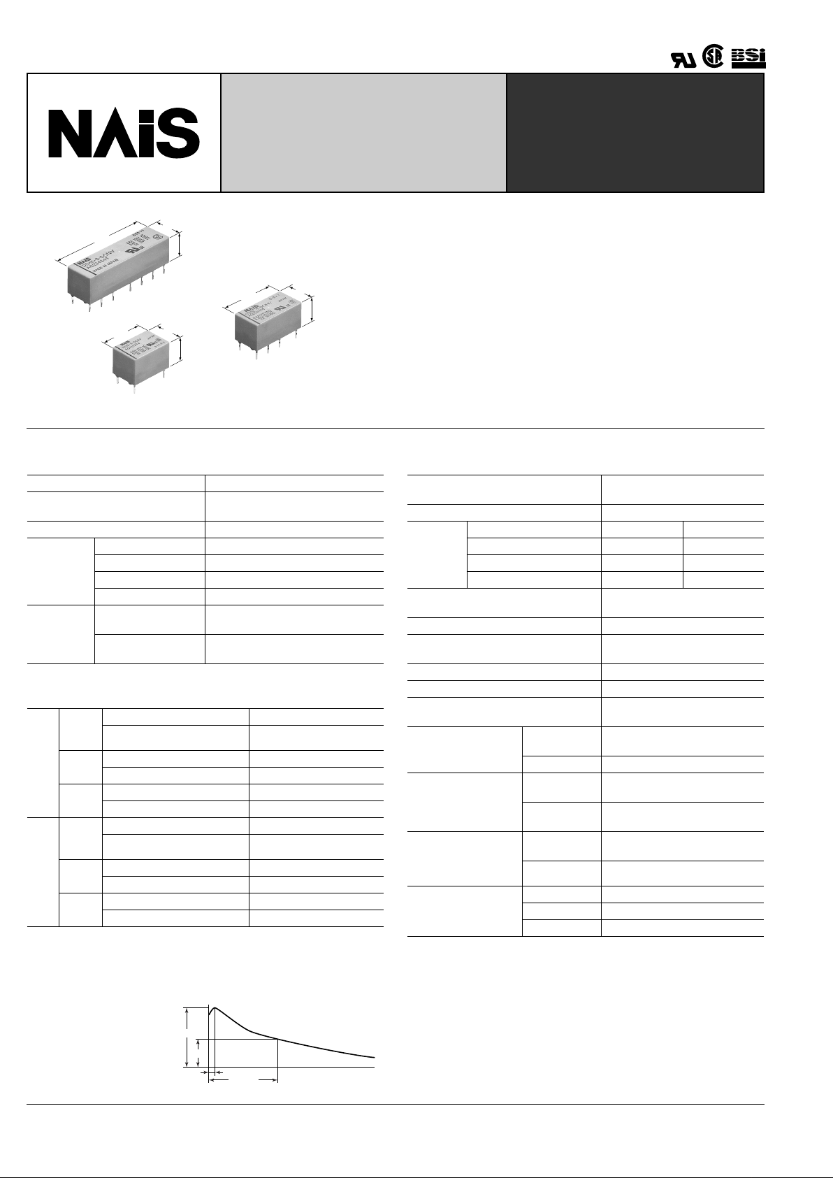
DS4E
35.24
1.387
9.9
.390
9.8
.386
DS1E
15
.590
9.9
.390
9.8
.386
DS2E
20
.787
9.9
.390
9.8
.386
FEATURES
• High sensitivity: 200 mW pick-up power
100 mW pick-up power types available
• Latching types available
• High switching capacity: 60 W, 125 V A
• High breakdown voltage: 1,500 V FCC surge between open contacts
1,000 V AC between open contacts
• DIP-1C type can be used with 14 pin IC socket
2C type can be used with 16 pin IC socket,
4C type can be used with 2 sets of 14 pin IC sockets
• Gold-cap silver palladium types available for 2 Form C type
• Bifurcated contacts are standard
SPECIFICATIONS
Contact
* Gold capped silver-palladium contact also available f or 2 F orm C 10
7
operations at
0.1 A 50 V DC resistive
Coil (polarized) (at 20 ° C 68 ° F)
* For 1 Form C high sensitive types.
Characteristics (at 20 ° C 68 ° F)
Arrangement 1 Form C, 2 Form C, 4 Form C
Initial contact resistance, max.
(By voltage drop 6 V DC 1 A)
50 m Ω
Contact material Gold-clad sliver
Rating
(resistive)
Max. switching power
60 W, 125 VA
Max. switching voltage
220 V DC, 250 V AC
Max. switching current
2 A DC, AC
Max. carrying current
3 A DC, AC
Expected
life (min.
operations)
Mechanical
(at 600 cpm)
10
8
(1 Form C 2 coil latching type: 10
7
)
Electrical
2 A 30 VDC resistive
5 × 10
5
M
type
Single
side
stable
Minimum operating power
Approx. 200 mW
Nominal operating power
Approx. 400 mW
1 coil
latching
Minimum set and reset power
Approx. 90 mW
Nominal set and reset power
Approx. 180 mW
2 coil
latching
Minimum set and reset power
Approx. 180 mW
Nominal set and reset power
Approx. 360 mW
S
type
Single
side
stable
Minimum operating power
Approx. 100 mW (128 mW)*
Nominal operating power
Approx. 200 mW
1 coil
latching
Minimum set and reset power
Approx. 45 mW (58 mW)*
Nominal set and reset power
Approx. 90 mW
2 coil
latching
Minimum set and reset power
Approx. 90 mW (115 mW)*
Nominal set and reset power
Approx. 180 mW
Max. operating speed
20 cpm at rated load
50 cps at low level load
Initial insuration resistance*
1
Min. 100 M Ω (at 500 V DC)
Initial
breakdown voltage*
2
Type of relay (DS1-S type) (Other types)
Between open contacts 500 Vrms 1,000 Vrms
Between contacts sets — 1,000 Vrms
Between contacts and coil
1,000 Vrms 1,500 Vrms
FCC surge voltage between contacts
and coil
1,500 V (Expect DS1-S type)
Operate time*
3
(at nominal voltage) Approx. 3 ms
Release time (without diode)*
3
(at
nominal voltage)
Approx. 2 ms
Set time*
3
(at nominal voltage) Approx. 3 ms
Reset time*
3
(at nominal voltage) Approx. 3 ms
Temperature rise
(at nominal voltage, Contact current: 2A)
Max. 65 ° C
Shock resistance
Functional*
4
1C, 2C:Min. 490 m/s
2
{50 G}
4C:Min. 294 m/s
2
{30 G}
Destructive*
5
Min. 980 m/s
2
{100 G}
Vibration resistance
Functional*
6
10 to 55 Hz
at double amplitude of 3.3 mm
Destructive
10 to 55 Hz
at double amplitude of 5 mm
Conditions for operation,
transport and storage*
7
(Not freezing and condensing at low temperature)
Ambient
temp.
–40 ° C to +70 ° C
–40 ° F to +158 ° F
Humidity 5 to 85% R.H.
Unit weight
1 Form C Approx. 3.2g .11oz
2 Form C Approx. 4g .14oz
4 Form C Approx. 7g .25oz
FCC (Federal Communication Commission) requests following standard as Breakdown Voltage
specification.
10 µs
1500V
750V
160 µs
Remarks
* Specifications will vary with foreign standards certification ratings.
*
1
Measurement at same location as "Initial breakdown voltage" section
*
2
Detection current: 10 mA
*
3
Excluding contact bounce time
*
4
Half-wave pulse of sine wave: 11ms; detection time: 10 µ s
*
5
Half-wave pulse of sine wave: 6ms
*
6
Detection time: 10 µ s
*
7
Refer to 5. Conditions for operation, transport and storage mentioned in
AMBIENT ENVIRONMENT (Page 61)
mm inch

DS
187
TYPICAL APPLICATIONS
• T elecomm unication equipment
• Office equipment
• Computer peripherals
• Security equipment
• Measuring instrumentation
ORDERING INFORMATION
Contact
arrangement
2Ex DS
1: 1 Form C
2: 2 Form C
4: 4 Form C
*Reverse polarity types available (add suffix-R). Standard packing: Carton: 50 pcs.; Case: 500 pcs.
E M R
*
L2 DC 48 V
Coil voltage
DC 1.5, 3,
5, 6, 9, 12,
24, 48 V
Classification
of type
E: Amber
sealed type
Sensitivity
M: 400 mW nominal
operating power
S: 200 mW nominal
operating power
Operating function
Nil: Single side stable
L: 1 coil latching
L2: 2 coil latching
TYPES
Single side stable
1 coil latching
2 coil latching
Notes:
1. Reverse polarity types available (add suffix-R).
2. Standard packing: carton: 50 pcs.; case: 500 pcs.
Nominal Voltage , V DC
Part No.
1 Form C 2 Form C 4 Form C
M
(400 mW)
type
1.5 DS1E-M-DC1.5V DS2E-M-DC1.5V DS4E-M-DC1.5V
3 DS1E-M-DC3V DS2E-M-DC3V DS4E-M-DC3V
5 DS1E-M-DC5V DS2E-M-DC5V DS4E-M-DC5V
6 DS1E-M-DC6V DS2E-M-DC6V DS4E-M-DC6V
9 DS1E-M-DC9V DS2E-M-DC9V DS4E-M-DC9V
12 DS1E-M-DC12V DS2E-M-DC12V DS4E-M-DC12V
24 DS1E-M-DC24V DS2E-M-DC24V DS4E-M-DC24V
48 DS1E-M-DC48V DS2E-M-DC48V DS4E-M-DC48V
S
(200 mW)
type
1.5 DS1E-S-DC1.5V DS2E-S-DC1.5V DS4E-S-DC1.5V
3 DS1E-S-DC3V DS2E-S-DC3V DS4E-S-DC3V
5 DS1E-S-DC5V DS2E-S-DC5V DS4E-S-DC5V
6 DS1E-S-DC6V DS2E-S-DC6V DS4E-S-DC6V
9 DS1E-S-DC9V DS2E-S-DC9V DS4E-S-DC9V
12 DS1E-S-DC12V DS2E-S-DC12V DS4E-S-DC12V
24 DS1E-S-DC24V DS2E-S-DC24V DS4E-S-DC24V
48 DS1E-S-DC48V DS2E-S-DC48V DS4E-S-DC48V
Nominal Voltage , V DC
Part No.
1 Form C 2 Form C 4 Form C
M
(180 mW)
type
1.5 DS1E-ML-DC1.5V DS2E-ML-DC1.5V DS4E-ML-DC1.5V
3 DS1E-ML-DC3V DS2E-ML-DC3V DS4E-ML-DC3V
5 DS1E-ML-DC5V DS2E-ML-DC5V DS4E-ML-DC5V
6 DS1E-ML-DC6V DS2E-ML-DC6V DS4E-ML-DC6V
9 DS1E-ML-DC9V DS2E-ML-DC9V DS4E-ML-DC9V
12 DS1E-ML-DC12V DS2E-ML-DC12V DS4E-ML-DC12V
24 DS1E-ML-DC24V DS2E-ML-DC24V DS4E-ML-DC24V
48 DS1E-ML-DC48V DS2E-ML-DC48V DS4E-ML-DC48V
S
(90 mW)
type
1.5 DS1E-SL-DC1.5V DS2E-SL-DC1.5V DS4E-SL-DC1.5V
3 DS1E-SL-DC3V DS2E-SL-DC3V DS4E-SL-DC3V
5 DS1E-SL-DC5V DS2E-SL-DC5V DS4E-SL-DC5V
6 DS1E-SL-DC6V DS2E-SL-DC6V DS4E-SL-DC6V
9 DS1E-SL-DC9V DS2E-SL-DC9V DS4E-SL-DC9V
12 DS1E-SL-DC12V DS2E-SL-DC12V DS4E-SL-DC12V
24 DS1E-SL-DC24V DS2E-SL-DC24V DS4E-SL-DC24V
48 DS1E-SL-DC48V DS2E-SL-DC48V DS4E-SL-DC48V
Nominal Voltage , V DC
Part No.
1 Form C 2 Form C 4 Form C
M
(360 mW)
type
1.5 DS1E-ML2-DC1.5V DS2E-ML2-DC1.5V DS4E-ML2-DC1.5V
3 DS1E-ML2-DC3V DS2E-ML2-DC3V DS4E-ML2-DC3V
5 DS1E-ML2-DC5V DS2E-ML2-DC5V DS4E-ML2-DC5V
6 DS1E-ML2-DC6V DS2E-ML2-DC6V DS4E-ML2-DC6V
9 DS1E-ML2-DC9V DS2E-ML2-DC9V DS4E-ML2-DC9V
12 DS1E-ML2-DC12V DS2E-ML2-DC12V DS4E-ML2-DC12V
24 DS1E-ML2-DC24V DS2E-ML2-DC24V DS4E-ML2-DC24V
48 DS1E-ML2-DC48V DS2E-ML2-DC48V DS4E-ML2-DC48V
S
(180 mW)
type
1.5 DS1E-SL2-DC1.5V DS2E-SL2-DC1.5V DS4E-SL2-DC1.5V
3 DS1E-SL2-DC3V DS2E-SL2-DC3V DS4E-SL2-DC3V
5 DS1E-SL2-DC5V DS2E-SL2-DC5V DS4E-SL2-DC5V
6 DS1E-SL2-DC6V DS2E-SL2-DC6V DS4E-SL2-DC6V
9 DS1E-SL2-DC9V DS2E-SL2-DC9V DS4E-SL2-DC9V
12 DS1E-SL2-DC12V DS2E-SL2-DC12V DS4E-SL2-DC12V
24 DS1E-SL2-DC24V DS2E-SL2-DC24V DS4E-SL2-DC24V
48 DS1E-SL2-DC48V DS2E-SL2-DC48V DS4E-SL2-DC48V

DS
188
COIL DATA
(at 20 ° C 68 ° F)
Single side stable
1 coil latching
2 coil latching
Nominal voltage,
V DC
Pick-up voltage, V DC (max.)
Drop-out
voltage, V DC
(min.)
Coil resistance, Ω ( ± 10%)
Maximum allowable,
V DC (at 50 ° C 122 ° F)
1 Form C 2, 4 Form C 1 Form C 2, 4 Form C
M
type
1.5 1.05 1.05 0.15 5.63 1.8 2.25
3 2.1 2.1 0.3 22.5 3.6 4.5
5 3.5 3.5 0.5 62.5 6 7.5
6 4.2 4.2 0.6 90 7.2 9
9 6.3 6.3 0.9 203 10.8 13.5
12 8.4 8.4 1.2 360 14.4 18
24 16.8 16.8 2.4 1440 28.8 36
48 33.6 33.6 4.8 5760 57.6 72
S
type
1.5 1.2 1.05 0.15 11.3 2.4 3
3 2.4 2.1 0.3 45 4.8 6
5 4.0 3.5 0.5 125 8.0 10
6 4.8 4.2 0.6 180 9.6 12
9 7.2 6.3 0.9 405 14.4 18
12 9.6 8.4 1.2 720 19.2 24
24 19.2 16.8 2.4 2880 28.4 48
48 38.6 33.6 4.8 11520 76.8 96
Nominal voltage, V DC
Reset Set, V DC (max.)
Coil resistance, Ω ( ± 10%)
Maximum allowable,
V DC (at 50 ° C 122 ° F)
1 Form C 2, 4 Form C 1 Form C 2, 4 Form C
M
type
1.5 1.05 1.05 12.5 1.8 2.25
3 2.1 2.1 50 3.6 4.5
5 3.5 3.5 139 6 7.5
6 4.2 4.2 200 7.2 9
9 6.3 6.3 450 10.8 13.5
12 8.4 8.4 800 14.4 18
24 16.8 16.8 3200 28.8 36
48 33.6 33.6 12800 57.6 72
S
type
1.5 1.2 1.05 25 2.4 3
3 2.4 2.1 100 4.8 6
5 4.0 3.5 278 8.0 10
6 4.8 4.2 400 9.6 12
9 7.2 6.3 900 14.4 18
12 9.6 8.4 1600 19.2 24
24 19.2 16.8 6400 38.4 48
48 38.4 33.6 25600 76.8 96
Nominal voltage, V DC
Reset Set, V DC (max.) Coil resistance, Ω ( ± 10%)
Maximum allowable,
V DC (at 50 ° C 122 ° F)
1 Form C 2,4 Form C Coil l Coil ll 1 Form C 2,4 Form C
M
type
1.5 1.05 1.05 6.25 1.8 2.25
3 2.1 2.1 25 3.6 4.5
5 3.5 3.5 69.4 6 7.5
6 4.2 4.2 100 7.2 9
9 6.3 6.3 225 10.8 13.5
12 8.4 8.4 400 14.4 18
24 16.8 16.8 1600 28.8 36
48 33.6 33.6 6400 57.6 72
S
type
1.5 1.2 1.05 12.5 2.4 3
3 2.4 2.1 50 4.8 6
5 4.0 3.5 139 8.0 10
6 4.8 4.2 200 9.6 12
9 7.2 6.3 450 14.4 18
12 9.6 8.4 800 19.2 24
24 19.2 16.8 3200 38.4 48
48 38.4 33.6 12800 76.8 96

DS
189
DIMENSIONS
mm inch
1 Form C
Single side stable, 1 coil latching, 2 coil latching
General tolerance: ± 0.3 ± .012
7.62
.300
5.6
.221
0.6
.024
5.08
.200
0.6
.024
3.4
.134
9.9
.340
9.3
.366
15
.590
5.08
.200
0.6
.024
15
.590
9.9
.390
7.62
.300
7.62
.300
PC board pattern (Copper-side view)
Single side stable, 1 coil latching 2 coil latching
Tolerance: ± 0.1 ± .004
2.54
.100
7.62
.300
2.54
.100
5-0.9 dia
5-.035 dia
2.54
.100
7.62
.300
2.54
.100
6-0.9 dia
6-.035 dia
Schematic (Bottom view)
Single side stable
Deenergized condition
1 coil latching
Diagram shows the "reset" position when terminals 1
and 6 are energized.
Energize with reverse polarity to transfer contacts.
2 coil latching
Diagram shows the "reset" position when terminals 3
and 6 are energized.
Energize terminals 1 and 3 to transfer contacts.
N.O.
12
1
+
6
–
N.C.10COM
7
•
A polarity bar showing the relay direction
can replace the schematic.
SET
12
1
–
6
+
RST10COM
7
SET
12
SET RST
1+3–6
+
RST10COM
7
2 Form C
Single side stable, 1 coil latching, 2 coil latching
General tolerance: ± 0.3 ± .012
5.08
.200
5.08
.200
0.6
.024
3.4
.134
9.9
.340
9.3
.366
20
.787
7.62
.300
9.9
.390
0.6
.024
7.62
.300
5.6
.221
5.08
.200
5.08
.200
5.08
.200
2.54
.100
0.6
.024
20
.787
PC board pattern (Copper-side view)
Single side stable, 1 coil latching 2 coil latching
Tolerance: ± 0.1 ± .00
4
2.54
.100
7.62
.300
2.54
.100
8-0.9 dia
8-.035 dia
matching 16 pin IC socket
2.54
.100
7.62
.300
2.54
.100
10-0.9 dia
10-.035 dia
Schematic (Bottom view)
Single side stable
Deenergized condition
1 coil latching
Diagram shows the "reset" position when terminals 1
and 16 are energized.
Energize with reverse polarity to transfer contacts.
2 coil latching
Diagram shows the "reset" position when terminals 2
and 15 are energized.
Energize terminals 1 and 16 to transfer contacts.
N.O.
8
9
N.O.13COM16–
N.C.6COM
4
11
N.C.
+
1
•
A polarity bar showing the relay direction
can replace the schematic.
SET
8
9
SET13COM16+
RST6COM
4
11
RST
–
1
Set
Reset
SET
8
9
SET13COM15–
RST6COM
4
11
RST
+
2
16
–
+
1

DS
190
4 Form C
Single side stable, 1 coil latching, 2 coil latching
General tolerance: ± 0.3 ± .012
2.54
.100
5.08
.200
5.08
.200
5.08
.200
5.08
.200
5.08
.200
0.6
.024
3.4
.134
9.9
.340
9.3
.366
35.24
1.387
7.62
.300
9.9
.390
0.6
.024
7.62
.300
5.6
.221
5.08
.200
5.08
.200
5.08
.200
5.08
.200
5.08
.200
5.08
.200
0.6
.024
35.24
1.387
PC board pattern (Copper-side view)
Single side stable, 1 coil latching 2 coil latching
Tolerance: ± 0.1 ± .004
7.62
.300
2.54
.100
2.54
.100
2.54 × 2
.100 × 2
2.54 × 2
.100 × 2
2.54 × 2
.100 × 2
2.54 × 2
.100 × 2
2.54 × 2
.100 × 2
2.54 × 3
.100 × 3
14-0.9 dia
14-.035 dia
7.62
.300
2.54
.100
2.54
.100
2.54 × 2
.100 × 2
2.54 × 2
.100 × 2
2.54 × 2
.100 × 2
2.54
.100
2.54 × 2
.100 × 2
2.54 × 2
.100 × 2
2.54 × 2
.100 × 2
16-0.9 dia
16-.035 dia
Schematic (Bottom view)
Single side stable
Deenergized condition
1 coil latching
Diagram shows the "reset" position when terminals 1
and 16 are energized.
Energize with reverse polarity to transfer contacts.
2 coil latching
Diagram shows the "reset" position when terminals 2
and 15 are energized.
Energize terminals 1 and 16 to transfer contacts.
N.O.
7
10
N.O.
N.O.
8
9
N.O.13COM16–
N.C.
5
COM
4
14
COM
COM
3
12
N.C.
N.C.
6
11
N.C.
+
1
•
A polarity bar showing the relay direction
can replace the schematic.
SET
7
10
SET
SET
8
9
SET13COM16–
RST
5
COM
4
14
COM
COM
3
12
RST
RST
6
11
RST
+
1
SET
7
10
SET
SET
8
9
SET13COM16–
RST
5
COM
4
14
COM
Reset
Set
COM
3
12
RST
RST
6
11
RST
+
1
15
–
+
2
REFERENCE DATA
1. Maximum switching capacity 2. Life curve (Resistive load) 3. Contact reliability for AC loads
Sample: DS2E-M-DC24V 10 pcs.
Cycle rate: 20 cpm.
Detection level: 200 mΩ
10mV
10V
100V
1,000V
10µA 100mA 1A
Switching current
Contact voltage
10
100
1,000
102
Switching current, A
No. of operations, ×10
4
30 V DC
125 V DC
0.1
0.2
0.5
1.0
2.0
5.0
10.0
30.0
50.0
70.0
95.0
99.0
99.9
100 100 1,000
1A 125V AC
0.5A 250V AC
0.3A 250V AC
0.5A 125V AC
No. of operations, ×10
4
Weibull
probability data
F(t), %
mm inch

DS
191
4-(1). Coil termperature rise
(2 Form C single side stable type)
Point measured: Inside the coil
Ambient temperature: 18° to 19°C 64° to 66°F
4-(2). Coil tempeature rise
(4 Form C single side stable type)
Point measured: Inside the coil
Ambient temperature: 17° to 18°C 63° to 64°F
4-(3). Coil temperature rise
(2 Form C 2 coil latching type)
Point measured: Inside the coil
Ambient temperature: 20° to 21°C 68° to 70°F
10
20
30
40
50
60
0
100 110
3A
2A
0A
Coil applied voltage, %V
Temperature rise, °C
10
20
30
40
50
60
0
100 110
3A
2A
0A
Coil applied voltage, %V
Temperature rise, °C
10
20
30
40
50
60
0
100 110
3A
2A
0A
Coil applied voltage, %V
Temperature rise, °C
Reset coil
Set coil
4-(4). Coil temperature rise
(4 Form C 2 coil latching type)
Point measured: Inside the coil
Ambient temperature: 20°C 68°F
5. Operate and release time characteristics
(2 Form C single side stable type)
T est condition: Without diode connected to coil in parallel
6-(1). Influence of adjuacent mounting
(1 Form C)
10
20
30
40
50
60
0
100 110
3A
2A
0A
Coil applied voltage, %V
Temperature rise, °C
Reset coil
Set coil
1
2
3
4
0
80 100 120
Release time (mean)
Operate time (mean)
Coil applied voltage, %
Operate and release time, ms
–10
0
10
–10
0
10
5
.197
10
.394
Inter-relay distance , mm inch
Pick-up voltage
Drop-out voltage
(1) (2) (3)
OFF OFF
ON ON
OFF OFF
ON ON
Rete of change, % Rete of change, %
6-(2). Influence of adjacent mounting
(2 Form C)
6-(3). Influence of adjacent mounting
(4 Form C)
–10
0
10
–10
0
10
5
.197
10
.394
OFF OFF
ON ON
OFF OFF
ON ON
Inter-relay distance , mm inch
Pick-up voltage
Drop-out voltage
(1) (2) (3)
Rete of change, % Rete of change, %
–80
–60
–40
–20
0
20
40
60
80
10
.394
20
.787
OFF OFF
ON ON
OFF OFF
ON ON
Inter-relay distance , mm inch
Pick-up voltage
(1) (2) (3)
Rete of change, %
–80
–60
–40
–20
0
20
40
60
80
10
.394
20
.787
OFF OFF
ON ON
OFF OFF
ON ON
Inter-relay distance , mm inch
Drop-out voltage
(1) (2) (3)
Rete of change, %
For Cautions for Use, see Relay Technical Information (Page 48 to 76).
9/1/2000 All Rights Reserved, © Copyright Matsushita Electric Works, Ltd.
Go To Online Catalog
 Loading...