

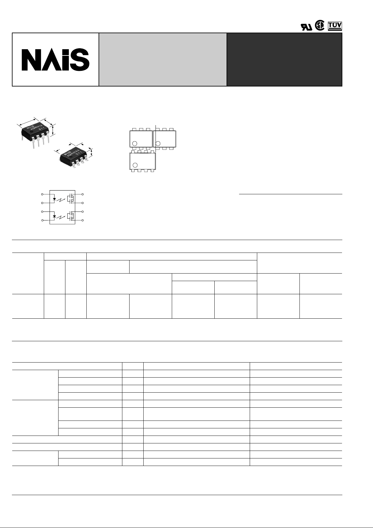
NAIS AQW414AZ, AQW414AX, AQW414A, AQW414 Datasheet
72
1
2
3
4
8
7
6
5
GU (General Use) Type
[2-Channel (Form B) Type]
mm inch
9.78
.385
6.4
.252
3.6±0.2
.142±.008
6.4
.252
9.78
.385
3.9±0.2
.154±.008
FEATURES
1. Approx. 1/2 the space compared
with the mounting of Two 1 Form B
photo MOS units
2. Applicable for 2 Form B use as well
as two independent 1 Form B use
3. Low thermal electromotive force
(Approx. 1 µ V)
4. Eliminates the need for a counter
electromotive force pr otection diode in
the drive circuits on the input side
Two 1 Form B units
2 Form B type
5. Controls load currents up to 0.13 A
with an input current of 5 mA
6. High speed switching: operate time
typical of 300 µ s
7. Eliminates the need for a po wer supply to drive the power MOSFET
8. Extremely low closed-circuit offset
voltages to enable control of small analog signals without distortion
9. Surface-mount model available
TYPICAL APPLICATIONS
• High-speed inspection machines
• T elephone equipment
• Computer
TYPES
*Indicate the peak AC and DC values.
Note: For space reasons, the package type indicator "X" and "Z" are omitted from the seal.
Type
Output rating* Part No.
Packing quantity
Load
voltage
Load
current
Through hole
terminal
Surface-mount terminal
Tube packing style
Tape and reel packing style
Tube Tape and reel
Picked from the
1/2/3-pin side
Picked from the
4/5/6-pin side
AC/DC type 400 V 100 mA AQW414 AQW414A AQW414AX AQW414AZ
1 tube contains
40 pcs.
1 batch contains
400 pcs.
1,000 pcs
RATINGS
1. Absolute maximum ratings (Ambient temperature: 25 ° C 77 ° F)
Item Symbol AQW414(A) Remarks
Input
LED forward current I
F
50 mA
LED reverse voltage V
R
3 V
Peak forward current I
FP
1 A f = 100 Hz, Duty factor = 0.1%
Power dissipation P
in
75 mW
Output
Load voltage V
L
400 V
Continuous load current I
L
0.1 A (0.13 A)
Peak AC, DC
( ): in case of using only 1 channel
Peak load current I
peak
0.3 A 100 ms (1 shot), V
L
= DC
Power dissipation P
out
800 mW
Total power dissipation P
T
850 mW
I/O isolation voltage V
iso
1,500 V AC
Temperature limits
Operating T
opr
–40 ° C to +85 ° C –40 ° F to +185 ° F Non-condensing at low temperatures
Storage T
stag
–40 ° C to +100 ° C –40 ° F to +212 ° F
PhotoMOS
RELAYS
AQW414
73
2. Electrical characteristics (Ambient temperature: 25 ° C 77 ° F)
Note: Recommendable LED forward current I
F
= 5 mA. For type of connection, see page 33.
*Operate/Reverse time
■
For Dimensions, see Page 27.
■
For Schematic and Wiring Diagrams, see Page 33.
■
For Cautions for Use, see Page 36.
Item Symbol AQW414(A) Condition
Input
LED operate (OFF) current
Typical
I
Foff
0.7 mA
I
L
= 100 mA
Maximum 3 mA
LED reverse (ON) current
Minimum
I
Fon
0.4 mA
I
L
= 100 mA
Typical 0.64 mA
LED dropout voltage
Typical
V
F
1.14 V (1.25 V at I
F
= 50 mA)
I
F
= 5 mA
Maximum 1.5 V
Output
On resistance
Typical
R
on
26 Ω
I
F
= 0 mA
I
L
= 100 mA
Within 1 s on time
Maximum 50 Ω
Off state leakage current Maximum I
Leak
1 µ
A
I
F
= 5 mA
V
L
= 400 V
Transfer
characteristics
Operate (OFF) time*
Typical
T
off
0.46 ms
I
F
= 0 mA ➝ 5 mA
I
L
= 100 mA
Maximum 1 ms
Reverse (ON) time*
Typical
T
on
0.40 ms
I
F
= 5 mA ➝ 0 mA
I
L
= 100 mA
Maximum 1 ms
I/O capacitance
Typical
C
iso
0.8 pF
f = 1 MHz
V
B
= 0
Maximum 1.5 pF
Initial I/O isolation resistance Minimum R
iso
1,000 M Ω
500 V DC
Toff
Input
Output
10%
90%
Ton
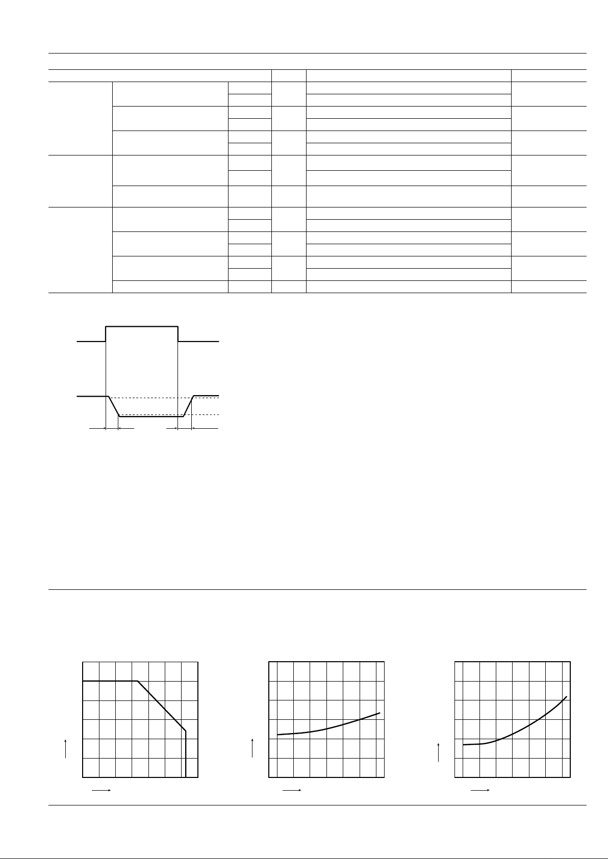
REFERENCE DATA
1. Load current vs. ambient temperature characteristics
Allowable ambient temperature: –40 ° C to +85 ° C
–40 ° F to +185 ° F
2. On resistance vs. ambient temperature characteristics
Measured portion: between terminals 5 and 6, 7 and 8;
LED current: 0 mA;
Continuous load current: 100 mA (DC)
3. Operate (OFF) time vs . ambient temper ature
characteristics
LED current: 5 mA;
Load voltage: 400 V (DC);
Continuous load current: 100 mA (DC)
0–20 20 40 60 100
100
80
60
40
20
0
–40 8085
Load current, mA
Ambient temperature, °C
0–20 20 40 60 8085
60
50
40
30
20
10
0
–40
On resistance, Ω
Ambient temperature, °C
0–20 20 40 60 8085
1.2
1.0
0.8
0.6
0.4
0.2
0
–40
Operate (OFF) time, ms
Ambient temperature, °C
 Loading...