

NAIS AQW227NAZ, AQW227NAX, AQW227NA, AQW227N, AQW225NAZ Datasheet
...
155
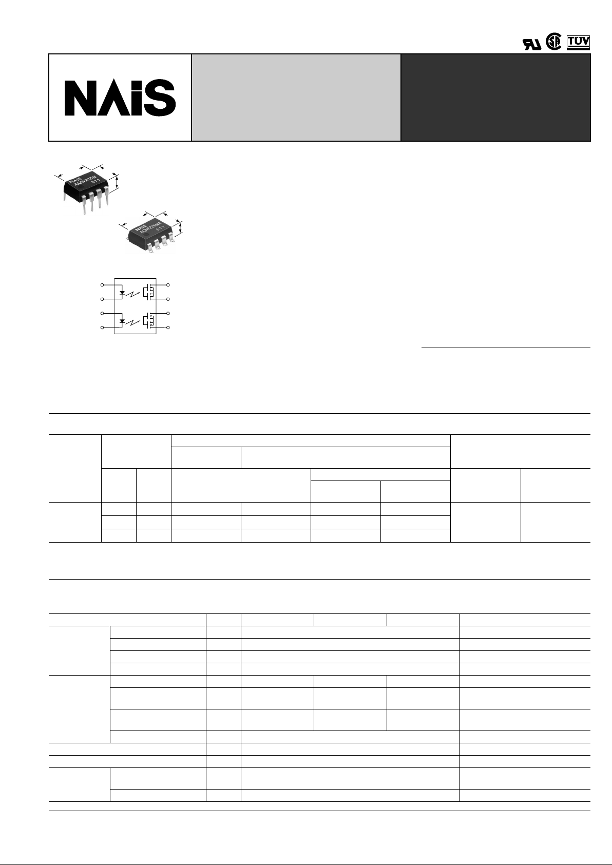
1
2
3
4
8
7
6
5
RF (Radio Frequency) Type
[2-Channel (Form A) Type]
—Low On resistance—
9.78
.385
6.4
.252
3.9±0.2
.154±.008
mm inch
9.78
.385
6.4
.252
3.6±0.2
.142±.008
FEATURES
1. PhotoMOS relay 2-channels (Form
A) type with high response speed, low
leakage current and low On resistance.
2. Applicable for 2 Form A use as well
as two independent 1 Form A use
3. Compact 8-pin DIP size
The device comes in a compact (W)
6.4 × (L) 9.78 × (H) 3.9 mm (W) .252 × (L)
.385 × (H) .154 inch , 8-pin DIP size
(through hole terminal type).
4. Low capacitance between output
terminals ensures high response
speed:
The capacitance between output terminals is small, typically 10 pF. This enables
for a fast operation speed of 200 µ s.
5. High sensitivity and low On resistance:
Maximum 0.16 A of load current can be
controlled with input current of 5 mA
(AQW225N). The 10 Ω On resistance is
less than our conventional models. With
no metallic contacts, the PhotoMOS relay
has stable switching characteristics.
6. Low-level off state leakage current:
The SSR has an off state leakage current
of several milliamperes , whereas the PhotoMOS relay has only 30 pA ev en with the
rated load voltage of 80 V (AQW225N).
7. Controls low-level analog signals:
PhotoMOS relay features extremely low
closed-circuit offset voltages to enable
control of small analog signals without
distortion.
8. Low terminals electromotive force:
(approx. 1 µ V)
TYPICAL APPLICATIONS
• Measuring equipment
• Scanner, IC checker, Board tester
TYPES
*Indicate the peak AC and DC values.
Note: For space reasons, the package type indicator "X" and "Z" are omitted from the seal.
Type
Output rating*
Part No.
Packing quantity
Through hole
terminal
Surface-mount terminal
Load
voltage
Load
current
Tube packing style
Tape and reel packing style
Tube Tape and reel
Picked from the
1/2/3-pin side
Picked from the
4/5/6-pin side
AC/DC type
80 V 120 mA AQW225N AQW225NA AQW225NAX AQW225NAZ
1 tube contains
40 pcs.
1 batch contains
400 pcs.
1,000 pcs.
200 V 50 mA AQW227N AQW227NA AQW227NAX AQW227NAZ
400 V 40 mA AQW224N AQW224NA AQW224NAX AQW224NAZ
RATING
1. Absolute maximum ratings (Ambient temperature: 25 ° C 77 ° F)
Item Symbol AQW225N(A) AQW227N(A) AQW224N(A) Remarks
Input
LED forward current I
F
50 mA
LED reverse voltage V
R
3 V
Peak forward current I
FP
1 A f = 100 Hz, Duty factor = 0.1%
Power dissipation P
in
75 mW
Output
Load voltage (peak AC) V
L
80 V 200 V 400 V
Continuous load current I
L
0.12 A
(0.16 A)
0.05 A
(0.07 A)
0.04 A
(0.05 A)
Peak AC, DC
( ): in case of using only 1 channel
Peak load current I
peak
0.36 A 0.15 A 0.12 A
A connection: 100 ms (1 shot),
V
L
= DC
Power dissipation P
out
800 mW
Total power dissipation P
T
850 mW
I/O isolation voltage V
iso
1,500 V AC
T emperature
limits
Operating T
opr
–40 ° C to +85 ° C –40 ° F to +185 ° F
Non-condensing at low
temperatures
Storage T
stg
–40 ° C to +100 ° C –40 ° F to +212 ° F
PhotoMOS
RELAYS

AQW22 ❍ N
156
2. Electrical characteristics (Ambient temperature: 25 ° C 77 ° F)
Note: Recommendable LED forward current I
F
= 5mA. For type of connection, see page 32.
*Turn on/Turn off time
■
For Dimensions, see Page 27.
■
For Schematic and Wiring Diagrams, see Page 32.
■
For Cautions for Use, see Page 36.
Item Symbol AQW225N(A) AQW227N(A) AQW224N(A) Remarks
Input
LED operate current
Typical
I
Fon
0.9 mA
I
L
= Max.
Maximum 3.0 mA
LED turn off current
Minimum
I
Foff
0.4 mA
I
L
= Max.
Typical 0.8 mA
LED dropout voltage
Typical
V
F
1.14 V (1.25 V at I
F
= 50 mA)
I
F
= 5 mA
Maximum 1.5 V
Output
On resistance
Typical
R
on
7 Ω
30 Ω
70 Ω
I
F
= 5 mA
I
L
= Max.
Within 1 s on time
Maximum 10 Ω
50 Ω
100 Ω
Output capacitance
Typical
C
out
10 pF
I
F
= 0
V
B
= 0
f = 1 MHz
Maximum 15 pF
Off state leakage current Maximum I
leak
10 nA
I
F
= 0
V
L
= Max.
Transfer
characteristics
Switching
speed
Turn on time*
Typical
T
on
0.20 ms
I
F
= 5 mA
I
L
= Max.
Maximum 0.5 ms
Turn off time*
Typical
T
off
0.08 ms
I
F
= 5 mA
I
L
= Max.
Maximum 0.2 ms
I/O capacitance
Typical
C
iso
0.8 pF
f = 1 MHz
V
B
= 0
Maximum 1.5 pF
Initial I/O isolation resistance Minimum R
iso
1,000 M Ω
500 V DC
Ton
Input
Output 10%
90%
Toff
REFERENCE DATA
1. Load current vs. ambient temperature characteristics
Allowable ambient temperature: –40 ° C to +85 ° C
–40 ° F to +185 ° F
2.-(1) On resistance vs. ambient temperature
characteristics
Measured portion: between terminals 5 and 6,
7 and 8; LED current: 5 mA; Load voltage: Max. (DC);
Continuous load current: Max. (DC)
2.-(2) On resistance vs. ambient temperature
characteristics
Measured portion: between terminals 5 and 6,
7 and 8; LED current: 5 mA; Load voltage: Max. (DC);
Continuous load current: Max. (DC)
0
60
80
140
0204060–20
8085
100–40
40
20
100
120
AQW225N
AQW227N
AQW224N
Load current, mA
Ambient temperature, °C
0
4.0
6.0
8.0
10.0
–40
12.0
0–20 20 40 60
8085
2.0
AQW225N
Ambient temperature, °C
On resistance, Ω
0
40
60
80
100
–40
120
0–20 20 40 60
8085
20
AQW224N
AQW227N
Ambient temperature, °C
On resistance, Ω
 Loading...