

1
P/N:PM0591 REV. 0.3, APR. 09, 1999
MX10C805X
SINGLE-CHIP 8-BIT MICROCONTROLLER
ADVANCED INFORMATION
FEATURE
• High performance CMOS ROM CPU
• Operation Voltage 5V
• Up to 40MHz operation (3.5MHz to 40MHz)
• Three 16-bit timer/counters
• 256 Bytes of on-chip data RAM
• 4/8/16/32/64 Kbytes on-chip Program memory
• 32 Programmable I/O lines
• On-chip Watch-Dog-Timer (WDT)
• 6 interrupt Sources
• ROM Code protection
• Two priority levels
• Power saving Idle and power down modes
• 64 K external program memory space
• 64 K external data memory space
• Available in PLCC, PQFP, and PDIP package
• Four 8-bit I/O ports
• Full-duplex enhanced UART compatible with the standard 80C51 and the 80C52
• Extended Temperature Range (-40°C to +85°C)
GENERAL DESCRIPTION
The single-chip 8-bit microcontroller is manufactured in
MXIC's advanced CMOS process. This de vice uses the
same powerful instruction set, has the same architecture, and is pin-to-pin compatible with the existing 80C51.
The added features make it an even more powerful
microcontroller for applications that require clock output, and up/down counting capabilities such as motor
control. It also has a more v ersatile serial channel that
facilitates multi-processor communications .
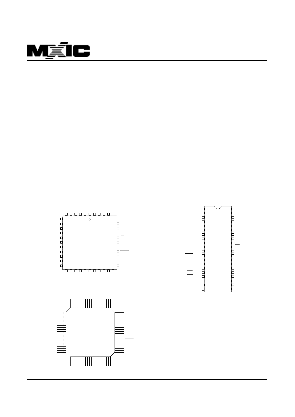
PIN CONFIGURATIONS
40 PDIP
44 PLCC
44 PQFP
MX10C805X
1
2
3
4
5
6
7
8
9
10
11
12
13
14
15
16
17
18
19
20
(T2) P1.0
(T2EX) P1.1
P1.2
P1.3
P1.4
P1.5
P1.6
P1.7
RESET
(RXD) P3.0
(TXD)P3.1
(INT0) P3.2
(INT1) P3.3
(T0) P3.4
(T1) P3.5
(WR) P3.6
(RD) P3.7
XTAL2
XTAL1
VSS
40
39
38
37
36
35
34
33
32
31
30
29
28
27
26
25
24
23
22
21
VCC
P0.0 (AD0)
P0.1 (AD1)
P0.2 (AD2)
P0.3 (AD3)
P0.4 (AD4)
P0.5 (AD5)
P0.6 (AD6)
P0.7 (AD7)
EA
ALE
PSEN
P2.7 (A15)
P2.6 (A14)
P2.5 (A13)
P2.4 (A12)
P2.3 (A11)
P2.2 (A10)
P2.1 (A9)
P2.0 (A8)
MX10C805X
P1.5
P1.6
P1.7
RST
P3.0
N.C.
P3.1
P3.2
P3.3
P3.4
P3.5
P0.4
P0.5
P0.6
P0.7
EA
N.C.
ALE
PSEN
P2.7
P2.6
P2.5
P1.4
P1.3
P1.2
P1.1
P1.0
N.C.
VCC
P0.0
P0.1
P0.2
P0.3
P3.6
P3.7
XTAL2
XTAL1
VSS
N.C.
P2.0
P2.1
P2.2
P2.3
P2.4
64440
39
34
29
7
12
17
18 23 28
1
1
11
12 22
23
33
34
44
P0.4
P0.5
P0.6
P0.7
EA
N.C.
ALE
PSEN
P2.7
P2.6
P2.5
P1.5
P1.6
P1.7
RST
P3.0
N.C.
P3.1
P3.2
P3.3
P3.4
P3.5
P1.4
P1.3
P1.2
P1.1
P1.0
N.C.
VCC
P0.0
P0.1
P0.2
P0.3
P3.6
P3.7
XTAL2
XTAL1
VSS
N.C.
P2.0
P2.1
P2.2
P2.3
P2.4
MX10C805X
2
P/N:PM0591
REV. 0.3, APR. 09, 1999
MX10C805X
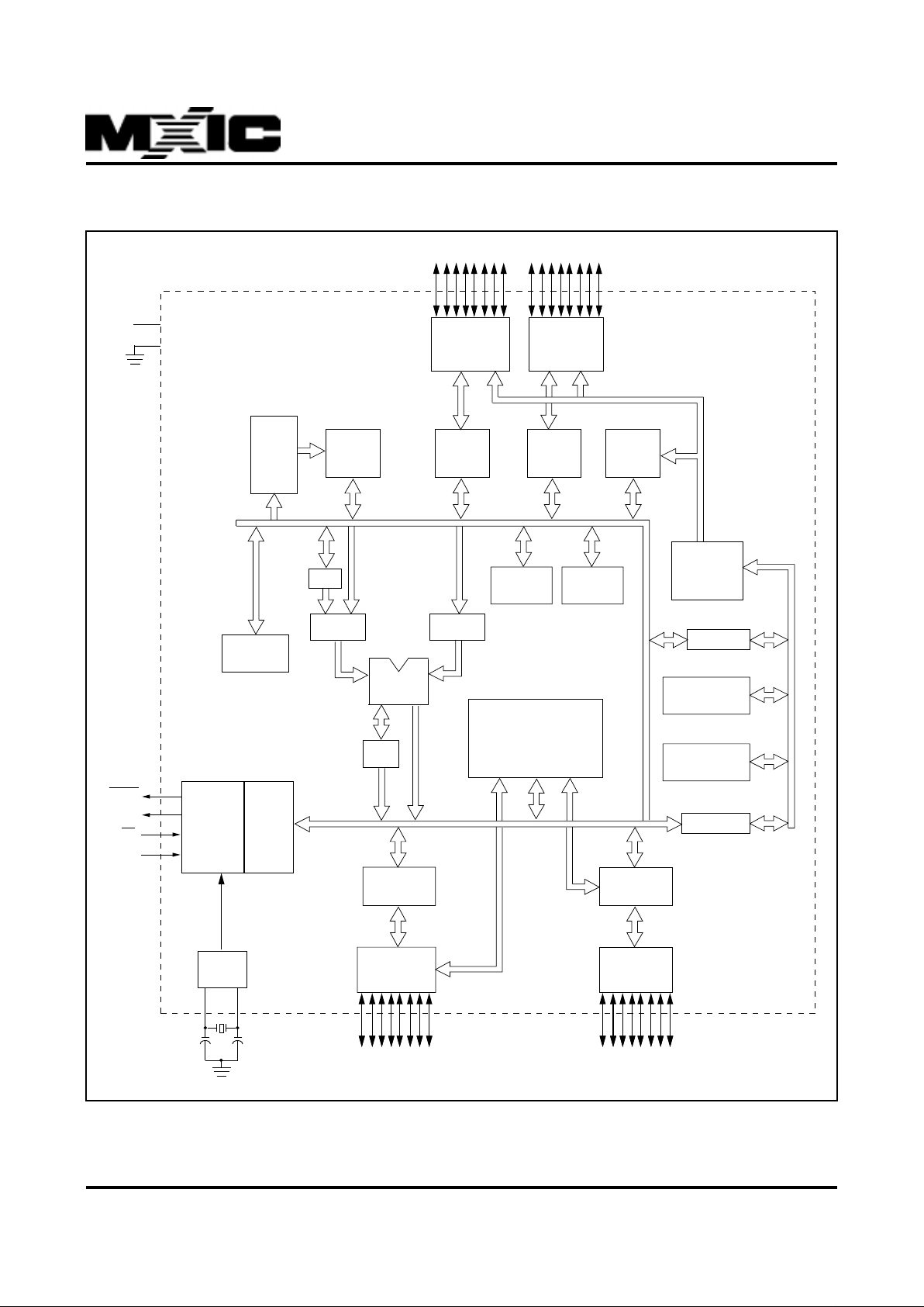
BLOCK DIAGRAM
PORT 0
DRIVERS
PORT 0
LATCH
ACC
PSW
TMP2
PORT 1
LATCH
PORT 1
DRIVERS
P1.0-P1.7
XTAL2
XTAL1
OSC.
TMP1
ALU
B
REGISTER
TIMING
AND
CONTROL
RAM
Vcc
Vss
RAM ADDR.
REGISTER
INSTRUCTION
REGISTER
PORT 2
LATCH
STACK
POINTER
ROM
PORT 2
DRIVERS
BUFFER
DPTR
PROGRAM
ADDR.
REGISTER
T0/T1/T2
SFRs
TIMERS
PORT 3
LATCH
PORT 3
DRIVERS
PC
INCREMENTER
PROGRAM
COUNTER
P0.0-P0.7 P2.0-P2.7
P3.0-P3.7
PSEN
ALE
EA
RST
T3
WATCHDOG
TIMER
3
P/N:PM0591
REV. 0.3, APR. 09, 1999
MX10C805X
PIN DESCRIPTIONS
VCC : Supply v oltage.
VSS : Circuit ground.
Port 0 : Port 0 is an 8-bit, open drain, bidirectional I/O
port. As an output port each pin can sink several LS
TTL inputs. Port 0 pins that have 1's written to them
float, and in that state can be used as high-impedance
inputs.
Port 0 is also the multiplex ed low-order address and data
bus during accesses to external Program and Data
Memory. In this application it uses strong internal pullups
when emitting 1's, and can source and sink serveral LS
TTL inputs.
Port 1 : P ort 1 is an 8-bit bidirectional I/O port with internal pullups. The port 1 output buffers can drive LS TTL
inputs. Port 1 pins that have 1's written to them are
pulled high by the internal pullups, and in that state can
be used as inputs. As inputs, P ort 1 pins that are externally pulled low will source current (IIL, on the data sheet)
because of the internal pullups.
In additional, Port 1 serves the functions of the following
special features of the MX10C805X :
Port Pin Alternate Function
P1.0 T2 (Exter nal Count Input to Timer/
Counter 2), Clock-Out
P1.1 T2EX (Timer/Counter 2 Capture/Reload
Trigger and Direction Control)
Port 2 : P ort 2 is an 8-bit bidirectional I/O port with internal pullups. The port 2 output buffers can drive LS TTL
inputs. Port 2 pins that have 1's written to them are
pulled high by the internal pullups, and in that state can
be used as inputs. As inputs, P ort 2 pins that are externally pulled low will source current (IIL, on the data sheet)
because of the internal pullups.
Port 2 emits the high-order address byte during fetches
from external Program Memory and during accesses to
external Data Memory that use 16-bit addresses (MOVX
@DPTR). In this application it uses strong internal
pullups when emitting 1's. During accesses to external
Data Memory that use 8-bit addresses (MOVX @Ri),
Port 2 emits the contents of the P2 Special Function
Register.
Port 3 : P ort 3 is an 8-bit bidirectional I/O port with internal pullups. The port 3 output buffers can drive LS TTL
inputs. Port 3 pins that have 1's written to them are
pulled high by the internal pullups, and in that state can
be used as inputs. As inputs, P ort 3 pins that are externally pulled low will source current (IIL, on the data sheet)
because of the internal pullups.
Port 3 also serves the function of various special features of the 8051 Family, as listed below :
Port Pin Alternate Function
P3.0 RXD (serial input port)
P3.1 TXD (serial output port)
P3.2 INT0 (external interrupt 0)
P3.3 INT1 (external interrupt 1)
P3.4 T0 (Timer 0 external input)
P3.5 T1 (Timer 1 external input)
P3.6 WR (external data memory write sttobe)
P3.7 RD (external data memory read strobe)
PROCESS INFORMATION
This device is manuf actured on a MXIC CMOS process.
P A CKAGES
MX10C805 1 P C
T emperature
C=0°C to 70°C
I=-40°C to 85°C
Package
P=PDIP
Q=PLCC
F=PQFP
ROM Size
0=64K Bytes
1=4K Bytes
2=8K Bytes
4=16K Bytes
8=32K Bytes
4
P/N:PM0591
REV. 0.3, APR. 09, 1999
MX10C805X
RST : Reset input. A high on this pin for two machine
cycles while the oscillator is running resets the device.
The port pins will be driven to their reset condition when
a minimum VIHI voltage is applied whether the oscillator is running or not. An internal pulldown resistor permits a power-on reset with only a capacitor connected
to VCC.
ALE : Address Latch Enable output pulse for latching
the low byte of the address during accesses to external
memory .
In normal operation ALE is emitted at a constant rate of
1/6 the oscillator frequency, and may be used for e xternal timing or clocking purposes. Note, however, that
one ALE pulse is skipped during each access to external Data Memory .
If desired, ALE operation can be disabled by setting bit
5 of SFR location 87H (PCON). With this bit set, the pin
is weakly pulled high. Howe ver, the ALE disab le feature
will be suspended during a MOVX or MO VC instruction,
idle mode, power do wn mode. The ALE disable f eature
will be terminated by reset. When the ALE disable f eature is suspended or terminated, the ALE pin will no
longer be pulled up weakly. Setting the ALE-disable bit
has no affect if the micrcontroller is in external execution mode.
Throughout the remainder of this data sheet, ALE will
refer to the signal coming out of the ALE pin, and the pin
will be referred to as the ALE pin.
PSEN : Progr am Store Enable is the read strobe to external Program Memory.
When the MX10C805X is executing code from e xternal
Program memory, PSEN is activated twice each machine cycle, except that two PSEN activations are
skipped during each access to external Data memory.
EA/VPP : Extrernal Access enable. EA must be str apped
to VSS in order to enable the twiceto fetch code from
external Program Memory locations 0000H to 0FFFFH.
EA will be internally latched on reset.
EA should be strapped to VCC f or internal program executions.
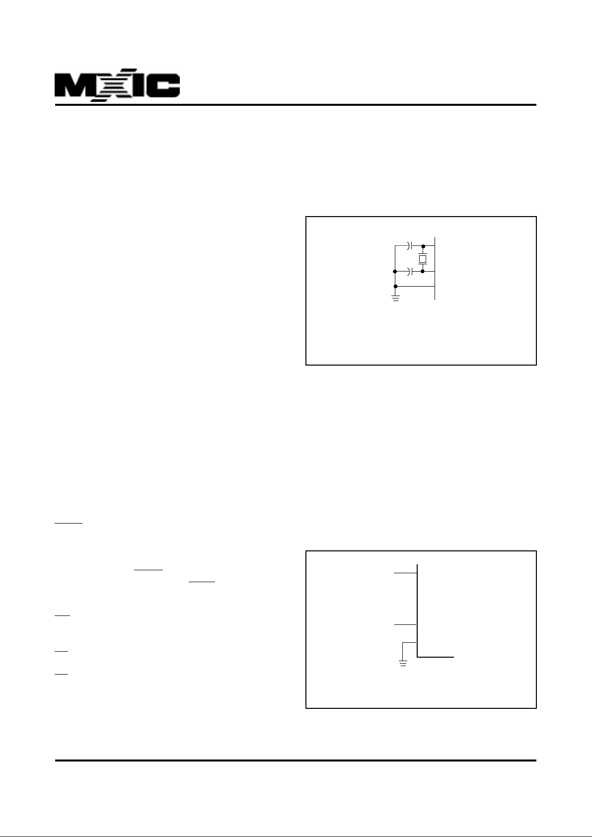
XTAL1 : Input to the inverting oscillator amplifier.
XTAL2 : Output from the inverting oscillator amplifier.
T o drive the de vice from an external clock source, XTAL1
should be driven, while XTAL2 floats, as shown in Figure 4. There are no requirememts on the duty cycle of
the external clock signal, since the input to the internal
clocking circuitry is through a divide-by-two flip-flop, b ut
minimum and maximum high and low times specified
on the data sheet must be observed.
An external oscillator may encounter as much as a 100
pF load at XTAL1 when it starts up. This is due to interaction between the amplifer and its feedback capacitance. Once the e xternal signal meets the VIL and VIH
specifications the capacitance will not exceed 20 pF.
C2
XTAL2
XTAL1
VSS
Figure 3. Oscillator Connections
C1, C2 = 30 pF is equal to or less than 10 pF for Crystal
For Ceramic Resonators,contact resonator manufacture.
C1
N/C
XTAL1
VSS
XTAL2
EXTERNAL
OSCILLATOR
SIGNAL
Figure 4. External Clock Drive Configuration
OSCILLA T OR CHARA CTERISTICS
XT AL1 and XTAL2 are the input and output, respectively ,
of a inverting amplifier which can be configured for use
as an on-chip oscillator, as sho wn in Figure 3. Either a
quartz crystal or ceramic resonator may be used.

5
P/N:PM0591
REV. 0.3, APR. 09, 1999
MX10C805X
T a ble 2. Status of the External Pins during Idle and Power Do wn
Mode Program Memory ALE PSEN PORT0 PORT1 PORT2 PORT3
Idle Internal 1 1 Data Data Data Data
Idle External 1 1 Float Data Address Data
Pow er Down Internal 0 0 Data Data Data Data
Pow er Down External 0 0 Float Data Data Data
POWER DOWN MODE
To save even more power, a Po wer Down mode can be
invok ed by software. If this mode, the oscillator is stopped
and the instruction that invoked Power Down is the last
instruction executed. The on-chip RAM and Special
Function Registers retain their values until the Power
Down mode is terminated.
On the MX10C805X either a hardware reset or an external interrupt can cause an exit from Power Down. Reset redefines all the SFRs but does not change the onchip RAM. An external interrupt allows both the SFRs
and on-chip RAM to retain their values.
ABSOLUTE MAXIMUM RATING*
Ambient Temperature Under Bias -40°C to +85°C
Storage T emperature -65°C to +150°C
Voltage on Any Other Pin to VSS -0.5V to +6.5V
IOL Per I/O Pin 15mA
Pow er Dissipation 1.5W
(Based on PACKAGE heat transfer limitations, not device consumption)
IDLE MODE
The user's software can invoke the Idle Mode. When
the microcontroller is in this mode, power consumption
is reduced. The Special Function Registers and the
onboard RAM retain their values during Idle, but the processor stops executing instructions. Idle Mode will be
exited if the chip is reset or if an enabled interrupt occurs.
OPERATING CONDITIONS
Symbol Description Min Max Units
TA Ambient Temperature Under Bias
Commerical 0 +70 °C
Industrial -40 +85 °C
VCC 4.5 5.5 V
fOSC Oscillator Frequency 3.5 40 MHz
To properly terminate Power Down, the reset or external interrupt should not be executed before VCC is restored to its normal operating level, and must be held
active long enough for the oscillator to restart and stabilize (normally less than 10 ms).
With an external interrupt, INT0 and INT1 must be enabled and configured as lev el-sensitive. Holding the pin
low restarts the oscillator but bringing the pin back high
completes the exit. Once the interrupt is serviced, the
next instruction to be executed after RETI will be the
one following the instruction that put the de vice into Power
Down.

6
P/N:PM0591
REV. 0.3, APR. 09, 1999
MX10C805X
DC CHARACTERISTICS (Over Operating Conditions)
All parameter values apply to all devices unless otherwise indicated.
Symbol Parameter Min Typ Max Unit Test Conditions
(Note 4)
VIL Input Low Voltage -0.5 0.2 VCC-0.1 V
VIL1 Input Low Voltage EA 0 0.2 VCC-0.3 V
VIH Input High Voltage 0.2 VCC+0.9 VCC+0.5 V
(Except XTAL1, RST)
VIH1 Input High Voltage 0.7 VCC VCC+0.5 V
(XTAL1, RST)
VOL Output Low Voltage (Note 5)
(Ports 1, 2, and 3) 0.4 V IOL=1.6 mA (Note 1)
VOL1 Output Low Voltage (Note 5)
(Port 0, ALE, PSEN) 0.4 V IOL=3.2 mA (Note 1)
VOH Output High Voltage 0.9 VDD V IOH=-10 uA
(Port 1, 2 and 3, ALE, PSEN) 0.75 VDD V IOH=-30 uA
0.5 VDD V IOH=-60uA
VOH1 Output High Voltage 0.9 VDD V IOH=-80 uA
(Port 0 in External Bus Mode) 0.75 VDD V IOH=-300 uA
0.5 VDD V IOH=-800 uA
IIL Logical 0 Input Current -50 uA VIN=0.4V
(Ports 1, 2 and 3)
ILI Input leakage Current (Port 0) ±10 uA VIN=VIL or VIH
ITL Logical 1 to 0 Transition Current -750 uA VIN=2V
(Ports 1, 2 and 3)
Industrial
PRST RST Pulldown Resistor 15 150 K ohm
CIO Pin Capacitance 10 pF @1 MHz, 25°C
ICC Power Supply Current: (Note 3)
Active Mode at 40 MHz 60 mA
Idle Mode at 40 MHz(70°C 5.5V) 28 mA
Power Down Mode 2 10 uA
NOTES:
1. Capacitive loading on Ports 0 and 2 may cause noise pulses above 0.4V to be superimposed on the VOLs of ALE and Ports 1, 2 and 3. The
noise is due to external bus capacitance discharging into the Port 0 and Port 2 pins when these pins change from 1 to 0. In applications
where capacitive loading exceeds 100 pF, the noise pulses on these signlas may exceed 0.8V. It may be desirable to qualify ALE or other
signals with a Schmitt Triggers, or CMOS-level input logic.
2. Capacitive loading on Ports 0 and 2 cause the VOH on ALE and PSEN to drop below the 0.9 VCC specification when the address lines are
stabilizing.
3. Minimum VCC for Power Down is 2V.
4. Typicals are based on a limited number of samples and are not guaranteed. The values listed are room temperature and 5V.
5. Under steady state (non-transient) conditions, IOL must be externally limited as follows:
Maximum IOL per port pin: 10mA
Maximum IOL per 8-bit port:
Port 0: 26mA
Ports 1, 2 and 3: 15mA
Maximum total IOL for all output pins: 71mA
If IOL exceeds the test condition, V OL ma y e xceed the related specification. Pins are not guaranteed to sink current greater than the listed test
conditions.

7
P/N:PM0591
REV. 0.3, APR. 09, 1999
MX10C805X
60.0
50.0
40.0
30.0
20.0
10.0
0.0
0.0
4.0
8.0
12.0
16.0
20.0
Freq at XTAL1 (MHz)
ICC (mA)
24.0
28.0 36.0
MAX
ACTIVE MODE
TYP
ACTIVE MODE
MAX
IDLE MODE
MAX
IDLE MODE
32.0
NOTE:
ICC Max at 33 MHz is at 5V is + 10% VCC, while
ICC Max at 24 MHz and below is at 5V + 20% VCC
Figure 5. 80C52/54/58 ICC vs Frequwncy
MX10C805X
RST
(NC)
CLOCK
SIGNAL
XTAL2
XTAL1
VSS
VCC
VCC
VCC
ICC
VCC
Figure 6. ICC Test Condition, Active Mode
All other pins disconnected
TCLCH = TCHCL = 5ns
P0
EA
MX10C805X
RST
(NC)
CLOCK
SIGNAL
XTAL2
XTAL1
VSS
VCC
VCC
VCC
ICC
Figure 7. ICC Test Condition Idle Mode
All other pins disconnected
TCLCH = TCHCL = 5ns
P0
EA

8
P/N:PM0591
REV. 0.3, APR. 09, 1999
MX10C805X
EXPLANATION OF THE AC SYMBOLS
Each timing symbol has 5 characters. The first character is always a "T" (stands for time). The other characters, depending on their positions, stand f or the name of
a signal or the logical status of that signal. The follo wing
is a list of all the characters and what they stand for.
A: Address
C: Cloc k
D: Input Data
H: Logic le v el HIGH
L: Logic level LOW, or ALE
P: PSEN
Q: Output Data
R: RD signal
T: Time
V: Valid
W: WR signal
X: No longer a v alid logic le vel
Z: Float
For example,
TAVLL = Time from Address Valid to ALE Low
TLLPL = Time from ALE Lo w to PSEN Low
MX10C805X
RST
(NC) XTAL2
XTAL1
VSS
VCC
VCC
VCC
ICC
Figure 8. ICC Test Condition, Power Down Mode
VCC=2.0V to 6.0V
All other pins disconnected
P0
EA
0.45V
0.2 VCC-0.1
TCHCL
TCLCX
TCLCL
TCLCH
TCHCX
VCC-0.5
0.7 VCC
Figure 9. Clock Signal Waveform for ICC Tests in Active and Idle Modes.
TCLCH = TCHCL = 5 ns

9
P/N:PM0591
REV. 0.3, APR. 09, 1999
MX10C805X
AC CHARA CTERISTICS
(Over Operating Conditions, Load Capacitance for P ort 0, ALE/PROG and PSEN = 100 pF, Load Capacitance for All
Other Outputs = 80 pF)
tCK min. = 1/f max. (maximum operating frequency); tCK=cloc k period
SYMBOL PARAMETER 33 MHz UNIT
MIN MAX
EXTERNAL PROGRAM MEMOR Y
TLHLL ALE PULSE DURATION 20 - NS
TAVLL ADDRESS SET-UP TIME TO ALE 17 - NS
TLLAX ADDRESS HOLD TIME AFTER ALE 10 - NS
TLLIV TIME FROM ALE TO VALID INSTRUCTION INPUT - 55 NS
TLLPL TIME FROM ALE TO CONTROL PULSE PSEN 17 - NS
TPLPH CONTROL PULSE DURA TION PSEN 70 - NS
TPLIV TIME FROM PSEN TO VALID INSTRUCTION INPUT - 12 NS
TPXIX INPUT INSTRUCTION HOLD TIME AFTER PSEN 0 - NS
TPXIZ INPUT INSTRUCTION FLOAT DELAY AFTER PSEN - 20 NS
T A VI V ADDRESS TO V ALID INSTRUCTION INPUT - 95 NS
TPLAZ TO PSEN ADDRESS FLOAT TIME - 10 NS
EXTERNAL DAT A MEMOR Y
TLHLL ALE PULSE DURATION 20 - NS
TAVLL ADDRESS SET-UP TIME TO ALE 17 - NS
TLLAX ADDRESS HOLD TIME AFTER ALE 10 - NS
TRLRH RD PULSE DURA TION 80 - NS
TWL WH WR PULSE DURA TION 80 - NS
TRLDV RD TO V ALID DAT A INPUT - 60 NS
TRHDX DATA HOLD TIME AFTER RD 0 - NS
TRHDZ D ATA FLOAT DELAY AFTER RD 32 - NS
TLLDV TIME FROM ALE TO VALID DATA INPUT - 90 NS
T A VD V ADDRESS T O V ALID INPUT - 105 NS
TLLWL TIME FROM ALE TO RD OR WR 40 1 4 0 NS
TAVWL TIME FROM ADDRESS T O RD OR WR 45 - NS
TWHLH TIME FROM RD OR WR HIGH T O ALE HIGH 10 55 NS
TQVWX D A TA VALID T O WR TRANSITION 10 - NS
TQVWH DATA SET-UP TIME BEFORE WR 125 - NS
TWHQX DATA HOLD TIME AFTER WR 10 - NS
TRLAZ ADDRESS FLOA T DELAY AFTER RD - 0 NS
NOTE:
1. The maximun operating frequency is limited to 40 MHz and the minimum to 3.5 MHz.

10
P/N:PM0591
REV. 0.3, APR. 09, 1999
MX10C805X
External clock drive XTAL
SYMBOL P ARAMETER VARIABLE CLOCK UNIT
MIN MAX
fCLK clock frequency 1.2 16 (tbf .) MHz
tCLCL clock period 63 833 ns
tCHCX HIGH time 20 tCK-tCLCX ns
tCLCX LO W time 20 tCK-tCHCX ns
tCLCH RISE time - 20 ns
tCHCL F ALL time - 20 ns
tCY cycle time (tCY = 12 tCK) 0.75 10 ms
SERIAL PORT CHARACTERISTICS
Serial Port Timing : Shift Register Mode
VDD = 5V±10%; VSS = 0V; Tamb=0°C; Load Capacitance = 80 pF
SYMBOL PARAMETER 33 MHz OSCILLATOR UNIT
MIN MAX
tXLXL Serial P ort clock cycle time 360 - ns
tQVXH Output data setup to clock rising edge 167 - ns
tXHQX Output data hold after clock rising edge 5 - ns
tXHDX Input data hold after clock rising edge 0 - ns
tXHD V Clock rising edge to input data valid - 167 ns
EXTERNAL CLOCK DRIVE WAVEFORM
AC TESTING INPUT, OUTPUT WAVEFORMS FLOAT WAVEFORM
0.45V
0.2 VCC-0.1
TCHCL
TCLCX
TCLCL
TCLCH
TCHCX
VCC-0.5
0.7 VCC
0.2 VCC+0.9
AC Inputs during testing are driven at VCC-0.5V for a
Logic "1" 0.45V for a Logic "0". Timing measurements
are made at VIH min for a Logic "1" and VIL max for a
Logic "0".
0.2 VCC-0.1
0.45V
VCC-0.5
VLOAD
TIMING REFERENCE
POINTS
VLOAD-0.1V
VLOAD+0.1V
VOL+0.1V
VOH-0.1V
For timing purposes a port pin is no longer floating when a 100 mV
change from load voltage occurs, and begins to float when a 100mV
change form the loaded VOH/VOL level occurs. IOL/IOH = + 20 mA
11
P/N:PM0591
REV. 0.3, APR. 09, 1999
MX10C805X
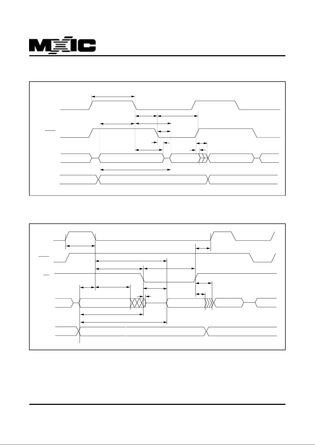
EXTERNAL PROGRAM MEMOR Y READ CYCLE
TLHLL
A8 - A15A8 - A15
A0 - A7A0 - A7 INSTR IN
ALE
PSEN
PORT 0
PORT 2
TLHIV
TPLIV
TPXIZ
TPLAZ
TPXIX
TLLAX
TAVIV
TPLIP
TLLPL
TAVLL
EXTERNAL DATA MEMORY READ CYCLE
DATA IN
A0-A7 FROM
PCL
A8-A15 FROM PCH
P2.0-P2.7 OR A8-A15 FROM DPH
A0-A7 FROM RI OR DPL
INSTR. IN
ALE
PSEN
PORT 0
PORT 2
TLHLL
TAVLL
TLLAX
TRLIZ
TAVWL
TRLRH
TWHLH
TRHDZ
TLLWL
TLLDL
TAVDV
TRHDX
TRLDV
RD
12
P/N:PM0591
REV. 0.3, APR. 09, 1999
MX10C805X
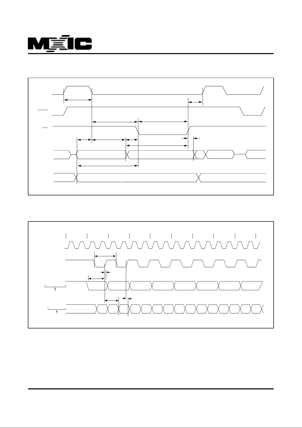
EXTERNAL DATA MEMORY WRITE CYCLE
DATA OUT
A0-A7 FROM
PCL
A8-A15 FROM PCH
P2.0-P2.7 OR A8-A15 FROM DPH
A0-A7 FROM RI OR DPL
INSTR. IN
ALE
PSEN
PORT 0
PORT 2
TLHLL
TAVLL
TLLAX
TAVWL
TWLWH
TWHLH
TLLWL
TQVWX
TWHQX
TQVWH
WR
SHIFT REGISTER MODE TIMING WAVEFORMS
ALE
CLOCK
OUTPUT DATA
WRITE TO SBUF
INPUT DATA
CLEAR RI
INSTRUCTION
0
0
VALID VALID VALID VALID VALID VALID VALID VALID
1
1
2
2
3
3
4
4
5
5
6
6
7
7
8
TXLXL
TXHQX
TXHDX
TQVXH
TXHDV

13
P/N:PM0591
REV. 0.3, APR. 09, 1999
MX10C805X
REVISION HISTORY
REVISION DESCRIPTION PAGE DATE
0.3 Modify Block Diagram P2 APR/09/1999

MACRONIX INTERNATIONAL CO., LTD.
HEADQUARTERS:
TEL:+886-3-578-6688
FAX:+886-3-563-2888
EUROPE OFFICE:
TEL:+32-2-456-8020
FAX:+32-2-456-8021
JAPAN OFFICE:
TEL:+81-44-246-9100
FAX:+81-44-246-9105
SINGAPORE OFFICE:
TEL:+65-348-8385
FAX:+65-348-8096
TAIPEI OFFICE:
TEL:+886-2-2509-3300
FAX:+886-2-2509-2200
MACRONIX AMERICA, INC.
TEL:+1-408-453-8088
FAX:+1-408-453-8488
CHICAGO OFFICE:
TEL:+1-847-963-1900
FAX:+1-847-963-1909
http : //www.macronix.com
MACRONIX INTERNATIONAL CO., LTD. reserves the right to change product and specifications without notice.
14
MX10C805X
 Loading...