

Page 1
Copyright © Murata Manufacturing Co., Ltd. All rights reserved. October 2017
MBN52832 Data Sheet, v1.5, 12/02/2020 www.murata.com
Revision History
Revision
Date
Author
Change Description
0.1
06/03/2016
RF PD
Preliminary version
0.2
06/16/2016
RF PD
Modified the module block diagram.
0.3
8/25/2016
RF PD
Update test data points
0.4
8/27/2016
RF PD
Update module dimension and reference schematic
0.5
12/15/2016
RF PD
Applied model/type name MBN52832 to the datasheet
0.6
02/01/2017
RF PD
Update Table 2.1 and Figure 2.2
0.7
03/15/2017
RF PD
Add sleep current
0.8
05/26/2017
RF PD
Table 2.2 change pin 36, 37 pin 36 description to NC.
Add section 6.1 and 6.2, recommendation for host PCB landing and
placement.
Updated reference schematic.
Add section 9 and section 10, assembly and packaging information.
Add section 12 Notice.
Add section 13 Preconditions to use the module.
0.9
07/27/2017
RF PD
Add regulatory section
0.92
8/23/2017
RF PD
Update layout guidance for antenna connection; updated regulatory
information
1.0
10/06/2017
Murata
Update the max height to 0.9mm, remove the sample part number.
1.1
06/14/2018
Murata
Remove Section 17, support contact.
1.2
10/10/2018
Murata
Added FCC and IC certification update for portable application in section
11.6
1.3
11/13/18
Murata
Corrected typos in section 7.
1.4
02/06/2020
Murata
Corrected module height in figure 2.1
Reformatted the content of section 2.3
Add KC certificate information. Fig 10.7; table 11.1; add section 11.7
1.5
12/02/2020
Murata
Corrected the TELEC ID in table 11.1
MBN52832 Data
BLE Module
Page 2

Copyright © Murata Manufacturing Co., Ltd. All rights reserved. October 2017
MBN52832 Data Sheet, v1.5, 12/02/2020 Page 2 of 34 www.murata.com
Table of Contents
REVISION HISTORY .............................................................................................................................................................. 1
TABLE OF CONTENTS ......................................................................................................................................................... 2
1 INTRODUCTION ............................................................................................................................................................ 5
1.1 Features ..................................................................................................................................................................... 5
1.2 Applications ................................................................................................................................................................ 5
1.3 Block Diagram ............................................................................................................................................................ 6
1.4 Acronyms ................................................................................................................................................................... 6
1.5 References ................................................................................................................................................................. 6
2 MECHANICAL SPECIFICATION .................................................................................................................................. 7
2.1 Module Dimensions .................................................................................................................................................... 7
2.2 Top and Side View ..................................................................................................................................................... 7
2.3 PCB Footprint Top View ............................................................................................................................................. 8
2.4 Pin Configuration ........................................................................................................................................................ 9
3 DC ELECTRICAL SPECIFICATION ............................................................................................................................ 12
3.1 Typical Power Consumption .................................................................................................................................... 12
4 RF SPECIFICATION .................................................................................................................................................... 12
5 ENVIRONMENTAL SPECIFICATION ......................................................................................................................... 13
5.1 Absolute Maximum Rating ....................................................................................................................................... 13
5.2 Recommended Operating Condition ........................................................................................................................ 13
6 POWER SEQUENCE ................................................................................................................................................... 13
7 APPLICATION INFORMATION ................................................................................................................................... 14
7.1 Recommended PCB Landing Pattern ...................................................................................................................... 14
7.2 Host PCB Layout Recommendations ...................................................................................................................... 15
7.3 Layout Guidance for Using Internal PCB Antenna .................................................................................................. 16
7.4 Layout Guidance for Microstrip Design And External Antenna ................................................................................ 17
8 APPLICATION REFERENCE ...................................................................................................................................... 20
9 ASSEMBLY INFORMATION ....................................................................................................................................... 21
10 PACKAGING AND MARKING INFORMATION .......................................................................................................... 22
10.1 Dimensions of Tape (Plastic tape) ........................................................................................................................... 22
10.2 Dimensions of Reel .................................................................................................................................................. 23
10.3 Taping Diagrams ...................................................................................................................................................... 24
10.4 Leader and Tail tape ................................................................................................................................................ 25
10.5 Peeling Force ........................................................................................................................................................... 26
10.6 PACKAGE (Humidity proof Packaging) ................................................................................................................... 26
10.7 Module Marking Information..................................................................................................................................... 27
10.8 Moisture Sensitivity Level ......................................................................................................................................... 27
11 REGULATORY INFORMATION .................................................................................................................................. 28
11.1 FCC Notice (USA) .................................................................................................................................................... 28
11.2 FCC Labeling Requirements .................................................................................................................................... 29
11.3 IC Notice (Canada) .................................................................................................................................................. 29
11.4 IC Labeling Requirements........................................................................................................................................ 30
11.5 ESTI compliance (Europe) ....................................................................................................................................... 30
11.6 RF Exposure ............................................................................................................................................................ 30
Page 3

Copyright © Murata Manufacturing Co., Ltd. All rights reserved. October 2017
MBN52832 Data Sheet, v1.5, 12/02/2020 Page 3 of 34 www.murata.com
11.6.1 Using on-board PCB antenna ..................................................................................................................... 30
11.6.2 Using external antenna ............................................................................................................................... 30
11.7 KC Certificate Notice ................................................................................................................................................ 30
12 ROHS INFORMATION ................................................................................................................................................. 31
13 ORDERING INFORMATION ........................................................................................................................................ 31
14 NOTICE ........................................................................................................................................................................ 32
14.1 Storage Conditions ................................................................................................................................................... 32
14.2 Handling Conditions ................................................................................................................................................. 32
14.3 Standard PCB Design (Land Pattern and Dimensions) ........................................................................................... 32
14.4 Notice for Chip Placer .............................................................................................................................................. 32
14.5 Operational Environment Conditions ....................................................................................................................... 32
14.6 Input Power Capacity ............................................................................................................................................... 33
15 PRECONDITIONS TO USE MURATA PRODUCTS ................................................................................................... 34
Page 4

Copyright © Murata Manufacturing Co., Ltd. All rights reserved. October 2017
MBN52832 Data Sheet, v1.5, 12/02/2020 Page 4 of 34 www.murata.com
LIST OF FIGURES
Figure 1.1 Block Diagram ........................................................................................................................................................ 6
Figure 2.1 Module Top and Side View (Unit: mm) .................................................................................................................. 7
Figure 2.2 Module Footprint Top View (Unit: mm) .................................................................................................................. 8
Figure 2.3 Pinout Diagram Top View ...................................................................................................................................... 9
Figure 7.1 Recommended PCB Landing Pattern.................................................................................................................. 14
Figure 7.2 Host PCB Layout Recommendation, top view ..................................................................................................... 15
Figure 7.3 Layout Guide for Antenna Performance (1) ......................................................................................................... 16
Figure 7.4 Layout Guide for Antenna Performance (2) ......................................................................................................... 17
Figure 7.5 Layout Guide for External Antenna (1) ................................................................................................................ 18
Figure 7.6 Layout Guide for External Antenna (2) ................................................................................................................ 18
Figure 8.1 Reference Design ................................................................................................................................................ 20
Figure 9.1 Reflow Profile ....................................................................................................................................................... 21
Figure 10.1 Tape Dimensions (Unit in mm) .......................................................................................................................... 22
Figure 10.2 Reel Dimensions (Unit: mm) .............................................................................................................................. 23
Figure 10.3 Tape Diagram .................................................................................................................................................... 24
Figure 10.4 Tape Leader and Tail ......................................................................................................................................... 25
Figure 10.5 Peeling Force Diagram ...................................................................................................................................... 26
Figure 10.6 Packaging Diagram............................................................................................................................................ 26
Figure 10.7 Module Marking Diagram ................................................................................................................................... 27
LIST OF TABLES
Table 2.1: Module Dimensions ................................................................................................................................................ 7
Table 2.2 Pinouts .................................................................................................................................................................. 10
Table 3.1 Typical Power Consumption ................................................................................................................................. 12
Table 4.1 RF Characteristics ................................................................................................................................................. 12
Table 5.1 Absolute Maximum Rating .................................................................................................................................... 13
Table 5.2 Recommended Operating Condition ..................................................................................................................... 13
Table 11.1 Regulatory Standards Conformance................................................................................................................... 28
Table 11.2 External Antenna to comply with FCC and IC .................................................................................................... 28
Table 11.3 External Antenna to comply with IC .................................................................................................................... 29
Page 5

Copyright © Murata Manufacturing Co., Ltd. All rights reserved. October 2017
MBN52832 Data Sheet, v1.5, 12/02/2020 Page 5 of 34 www.murata.com
1 Introduction
MBN52832 is a Bluetooth Low Energy module. It enables ultra-low power connectivity for data communication. The product
integrates Nordic Bluetooth Low Energy IC, RF front end, and crystal. This is an ideal solution for Internet of Things (IOT)
application.
1.1 Features
• Bluetooth® v5
o Higher throughput
o Increased broadcast capacity
o Improved channel co-existence algorithm (SCA)
• ANT, NFC Tag
• Nordic nRF52832 Bluetooth Smart®
• Built-in ARM Cortex M4 core with 64KB RAM and 512KB flash
• Dimension 7.4 x 7.0 x 0.9 mm
• Packaging: LGA
• Bluetooth/ANT Antenna Configuration:
o On-board PCB antenna
o Supports external antenna from pin pad
• Maximum transmit power: +4dBm @ antenna port (LDO Mode)
• Receive sensitivity: -93dBm @ 1Mbps (LDO Mode)
• Power consumption
o TX 7mA @ 3.5dBm (DCDC Mode)
o RX 6mA (DCDC Mode)
• Host interface: UART, SPI
• Other interfaces: 20 GPIO, 5 ADC, UART, SPI (master and slave), I2C, PWM and Debug SWD
• Operating temperature range: -40 ºC to 85 ºC
• RoHS compliant
• MSL Level 3 in accordance with JEDEC J-STD-020
• Regulatory certificates: FCC, IC, ETSI (plan)
1.2 Applications
• Home Automation
• Proximity Services
• Building automation
• Medical/Healthcare
• Beacon
Page 6
Copyright © Murata Manufacturing Co., Ltd. All rights reserved. October 2017
MBN52832 Data Sheet, v1.5, 12/02/2020 Page 6 of 34 www.murata.com
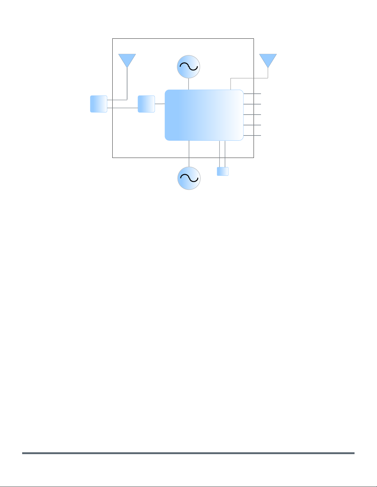
1.3 Block Diagram
Figure 1.1 Block Diagram
1.4 Acronyms
- AIO Analog Input / Output
- GPIO General Purpose Input / Output
- I2C Inter-Integrated Circuit
- LPCOMP Low Power Comparator
- SPI Serial Peripheral Interface
- UART Universal Asynchronous Receiver Transmitter
1.5 References
[1] Nordic Semiconductor, nRF52832 - Product Specification v1.3, 2017
[2] Nordic Semiconductor, nRF52832-CIAA Pin assignment and mechanical dimensions, 2016
VCC
UART
SWD
GPIO/AIO
SPI
Nordic
nRF52832
32MHz X’tal
Matching
circuit
32KHz X’tal
(for ANT only
NFC Antenna
(Optional)
BLE/ANT
Antenna
To external or
on-board
antenna
Inductor for DC/DC
(optional)
Page 7
Copyright © Murata Manufacturing Co., Ltd. All rights reserved. October 2017
MBN52832 Data Sheet, v1.5, 12/02/2020 Page 7 of 34 www.murata.com
2 Mechanical Specification
2.1 Module Dimensions
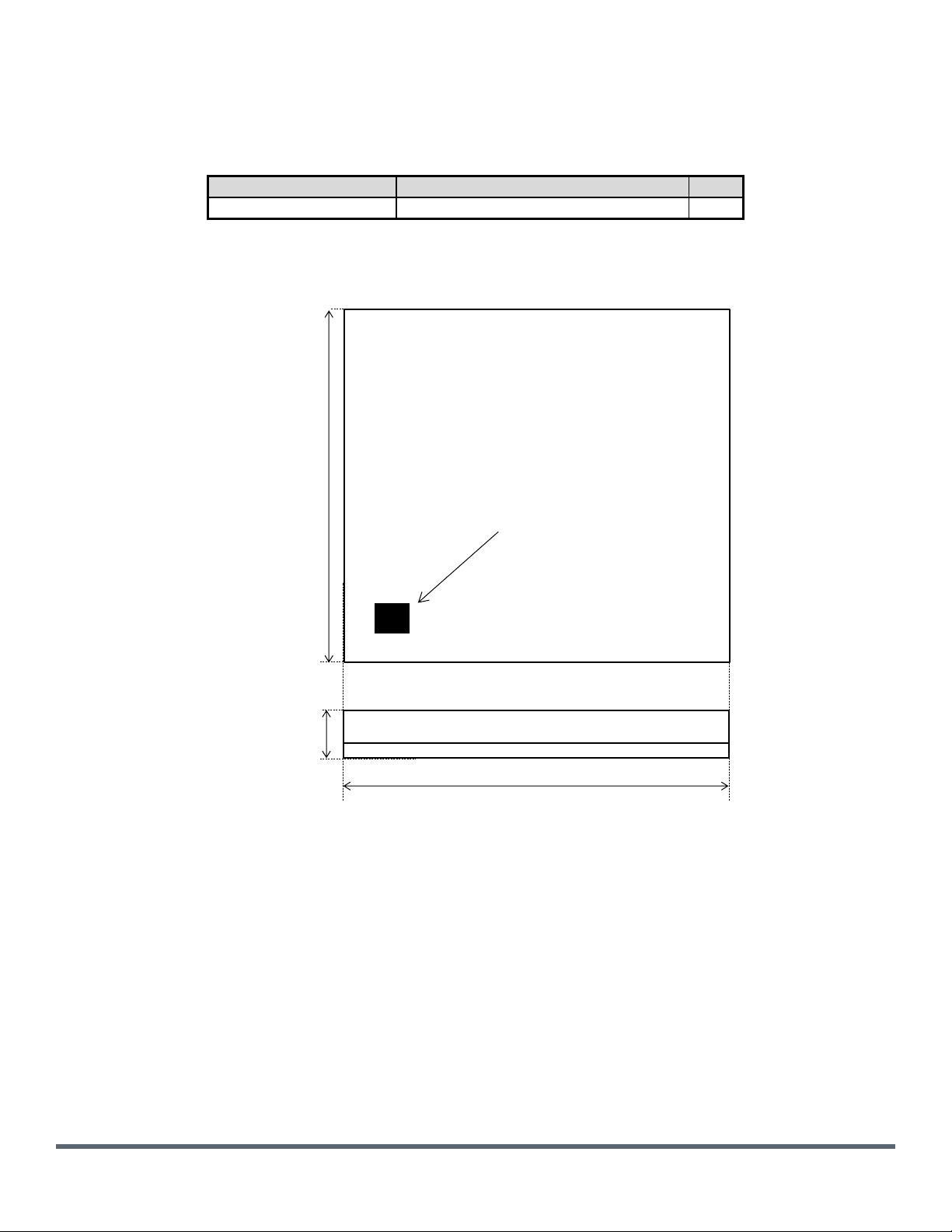
Table 2.1: Module Dimensions
Parameter
Typical
Unit
Dimension (L x W x H)
7.4 ±0.2mm x 7.0 ±0.2mm x 0.9 (max)
mm
2.2 Top and Side View
Figure 2.1 Module Top and Side View (Unit: mm)
Pin 1
7.0mm typ.
0.9mm
max.
7.4mm typ.
Page 8
Copyright © Murata Manufacturing Co., Ltd. All rights reserved. October 2017
MBN52832 Data Sheet, v1.5, 12/02/2020 Page 8 of 34 www.murata.com
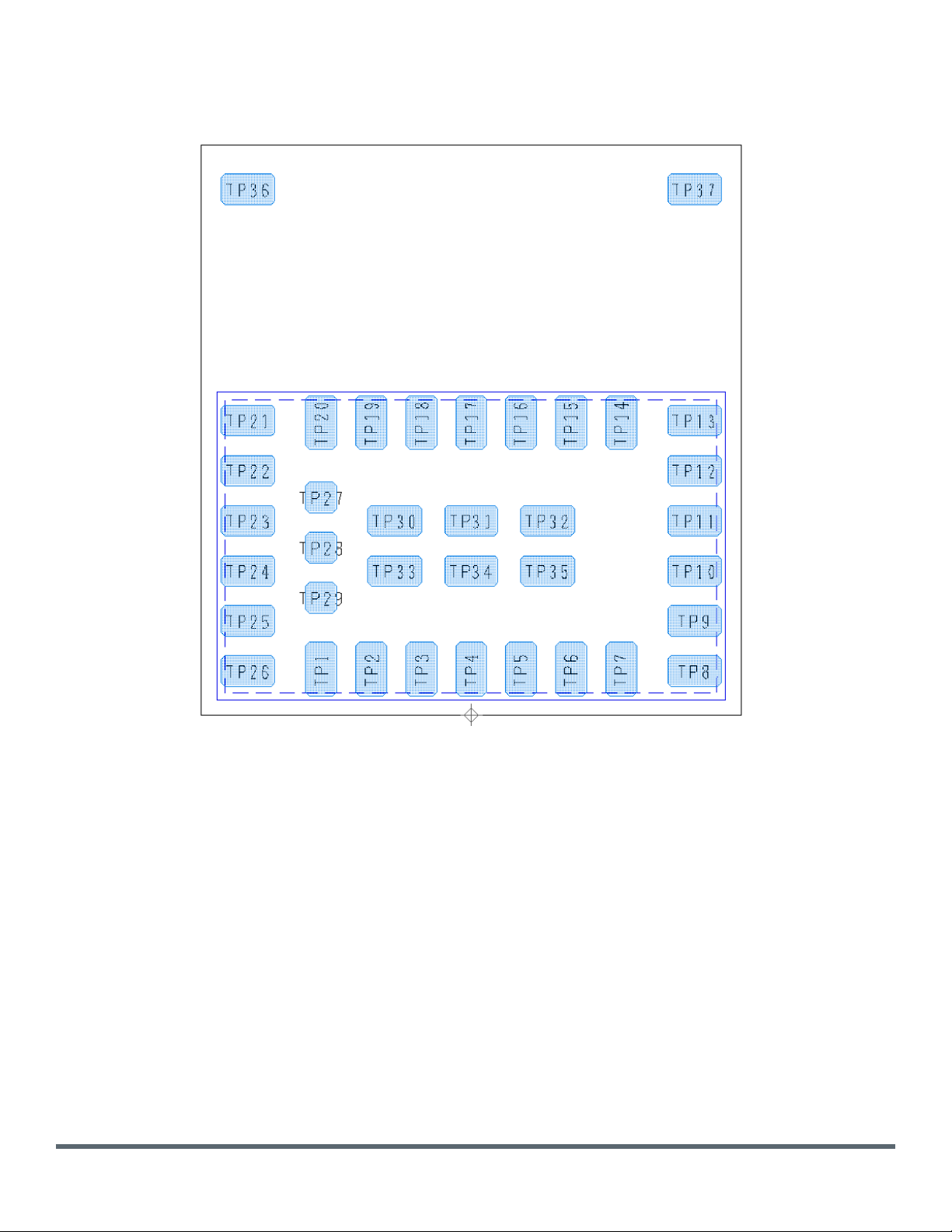
2.3 PCB Footprint Top View
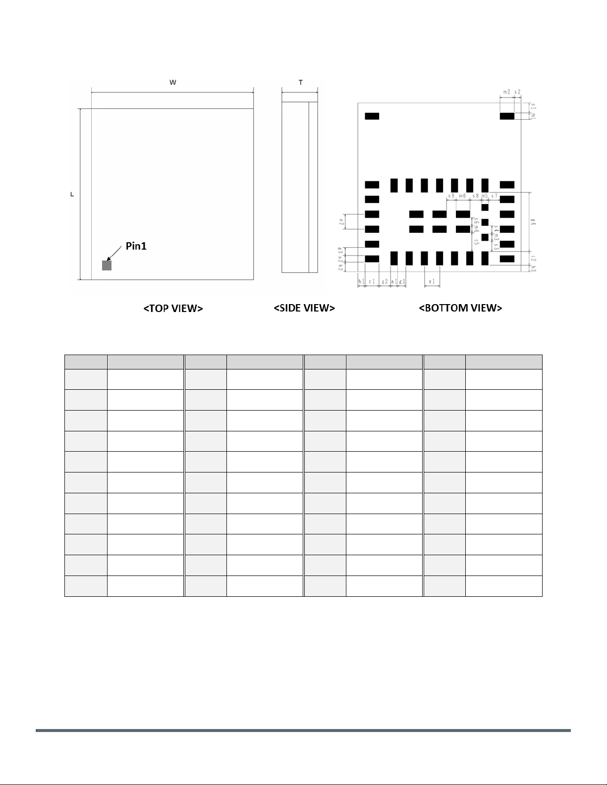
Figure 2.2 Module Footprint Top View (Unit: mm)
Mark
Dimensions
Mark
Dimensions
Mark
Dimensions
Mark
Dimensions
L
7.4±0.2
W
7.0±0.2
T
0.9 MAX
a1
0.3±0.1
a2
0.3±0.1
b1
0.3±0.2
b2
0.425±0.2
b3
0.3±0.2
c1
0.6±0.1
c2
0.6±0.1
e1
0.65±0.1
e2
0.65±0.1
g1
0.35±0.1
g2
0.5±0.1
g3
0.35±0.1
g4
2.6±0.1
m1
0.3±0.1
m2
0.6±0.1
m3
0.3±0.1
m4
0.3±0.1
m5
0.3±0.1
m6
0.6±0.1
s1
0.425±0.2
s2
0.3±0.2
s3
0.475±0.1
s4
0.35±0.1
s5
0.825±0.1
s6
0.35±0.1
s7
0.5±0.1
s8
0.5±0.1
s9
0.4±0.1
Page 9
Copyright © Murata Manufacturing Co., Ltd. All rights reserved. October 2017
MBN52832 Data Sheet, v1.5, 12/02/2020 Page 9 of 34 www.murata.com
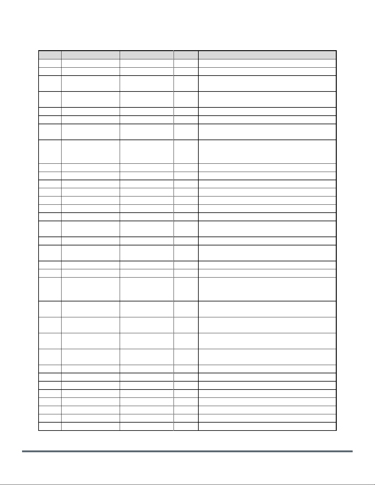
2.4 Pin Configuration
Figure 2.3 Pinout Diagram Top View
Page 10
Copyright © Murata Manufacturing Co., Ltd. All rights reserved. October 2017
MBN52832 Data Sheet, v1.5, 12/02/2020 Page 10 of 34 www.murata.com
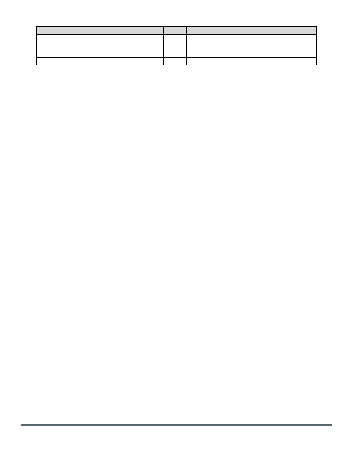
Table 2.2 Pinouts
Pin #
Pin Name
Nordic IC Pin
I/O
Description
1
P0_09/NFC ANT
P0.09/NFC
I/O
GPIO; NFC antenna connection.
2
P0_06
P0.06
I/O
GPIO
3
P0_00/XL1
P0.00/XL1
I/O
Connection for 32.768kHz crystal (LFXO);
GPIO
4
P0_01/XL2
P0.01/XL2
I/O
Connection for 32.768kHz crystal (LFXO);
GPIO
5
GND
GND
6
VCC
VDD
Module power supply
7
DCC
DCC
DC/DC converter output pin. *Refer to
reference schematic.
8
DEC
DEC4
1V3 regulator supply decoupling. Input from
DC/DC converter. Output from 1.3V LDO.
*Refer to reference schematic.
9
P0_02/AIN0
P0.02/AIN0
I/O
GPIO; SAADC/COMP/LPCOMP input
10
P0_05/AIN3
P0.05/AIN3
I/O
GPIO; SAADC/COMP/LPCOMP input
11
P0_03/AIN1
P0.03/AIN1
I/O
GPIO; SAADC/COMP/LPCOMP input
12
P0_04/AIN2
P0.04/AIN2
I/O
GPIO; SAADC/COMP/LPCOMP input
13
P0_29/AIN5
P0.29/AIN5
I/O
GPIO; SAADC/COMP/LPCOMP input
14
P0_07
P0.07
I/O
GPIO
15
P0_08
P0.08
I/O
GPIO
16
SWDIO
SWDIO
I/O
Serial Wire Debug I/O for debug and
programming.
17
P0_21/RESET
P0.21/RESET
I/O
GPIO; Configurable as system RESET pin
18
SWDCLK
SWDCLK
I/O
Serial Wire Debug clock input for debug
and programming.
19
GND
GND
GND
20
ANTIN
*Refer to reference schematic.
21
ANTOUT
RF signal output. Connect to ANTIN for onboard antenna or to external antenna.
*Refer to reference schematic.
22
P0_18/TRACE0
P0.18/TRACE
DATA[0]
I/O
GPIO; Trace port output;
23
P0_16/TRACE1
P0.16/TRACE
DATA[1]
I/O
GPIO; Trace port output.
24
P0_15/TRACE2
P0.15/TRACE
DATA[2]
I/O
GPIO; Trace port output.
25
P0_14/TRACE3
P0.14/TRACE
DATA[3]
I/O
GPIO; Trace port output.
26
P0_10/NFC ANT
P0.10/NFC
I/O
GPIO; NFC antenna connection.
27
P0_20
P0.20
I/O
GPIO
28
P0_17
P0.17
I/O
GPIO
29
P0_13
P0.13
I/O
GPIO
30
GND
Ground.
31
GND
Ground.
32
GND
Ground.
33
GND
Ground.
Page 11
Copyright © Murata Manufacturing Co., Ltd. All rights reserved. October 2017
MBN52832 Data Sheet, v1.5, 12/02/2020 Page 11 of 34 www.murata.com
Pin #
Pin Name
Nordic IC Pin
I/O
Description
34
GND
Ground.
35
GND
Ground.
36
NC
NC
37
NC
NC
Page 12
Copyright © Murata Manufacturing Co., Ltd. All rights reserved. October 2017
MBN52832 Data Sheet, v1.5, 12/02/2020 Page 12 of 34 www.murata.com
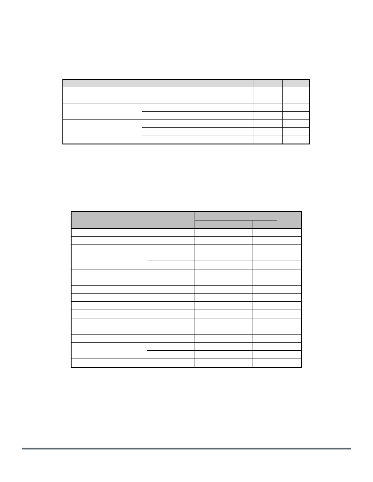
3 DC Electrical Specification
3.1 Typical Power Consumption
Table 3.1 Typical Power Consumption
Current
Unit
TX Active @3.5dBm
LDO mode
16
mA
DCDC mode
7
mA
RX Active
LDO mode
14
mA
DCDC mode
6
mA
Sleep Mode
System Off
0.36
uA
System On with internal RC
2.13
uA
System On with external 32kHz crystal
1.79
uA
4 RF Specification
Conditions: 25ºC, VCC=3.3V, Parameters measured at RF connector.
Table 4.1 RF Characteristics
RF Characteristics
Specification
Unit
Min.
Typ.
Max.
Center frequency
2402
-
2480
MHz
Channel Spacing
- 2 -
MHz
Number of RF Channels
-
40 - -
Max output power
LDO mode
-
4.0
-
dBm
DCDC mode
3.5
dBm
Modulation Characteristics
Δf1
avg
225
-
275
kHz
Δf2
max
(at 99.9%)
185 - -
kHz
Δf2
avg
/ Δf1
avg
0.8 - -
-
Carrier frequency offset and drift
1) Frequency offset: | fn – fTX |
- - 150
kHz
2) Frequency drift: | f0 – fn |
- - 50
kHz
3) Drift rate #0: | f1 – f0 |
- - 20
kHz
4) Drift rate #n: | fn – f
n-5
|
- - 20
kHz
Receiver sensitivity (PER
< 30.8%)
LDO mode
-
-93
-70
dBm
DCDC mode
-90
-70
dBm
Maximum input signal level (PER < 30.8%)
-10 - -
dBm
Page 13
Copyright © Murata Manufacturing Co., Ltd. All rights reserved. October 2017
MBN52832 Data Sheet, v1.5, 12/02/2020 Page 13 of 34 www.murata.com
5 Environmental Specification
5.1 Absolute Maximum Rating
Table 5.1 Absolute Maximum Rating
Description
Min
Max
Unit
Storage temperature
-40
+125
°C
Operating temperature
-40
85
°C
VCC
-0.3
+3.9
V
VIO, VDD ≤ 3.6 V
-0.3
VCC+0.3
V
VIO, VDD > 3.6 V
-0.3
3.9
V
NFC antenna pin current
80
mA
RF input level
10
dBm
5.2 Recommended Operating Condition
Table 5.2 Recommended Operating Condition
Parameter
Min
Max
Unit
Operating Temperature Range
-40
85
°C
VCC
1.7
3.6
V
Supply rise time (0V to 1.7V)
60
ms
6 Power Sequence
For device start up sequence, please refer to Nordic Semiconductor, nRF52832 - Product Specification [1].
Page 14
Copyright © Murata Manufacturing Co., Ltd. All rights reserved. October 2017
MBN52832 Data Sheet, v1.5, 12/02/2020 Page 14 of 34 www.murata.com
7 Application Information
7.1 Recommended PCB Landing Pattern
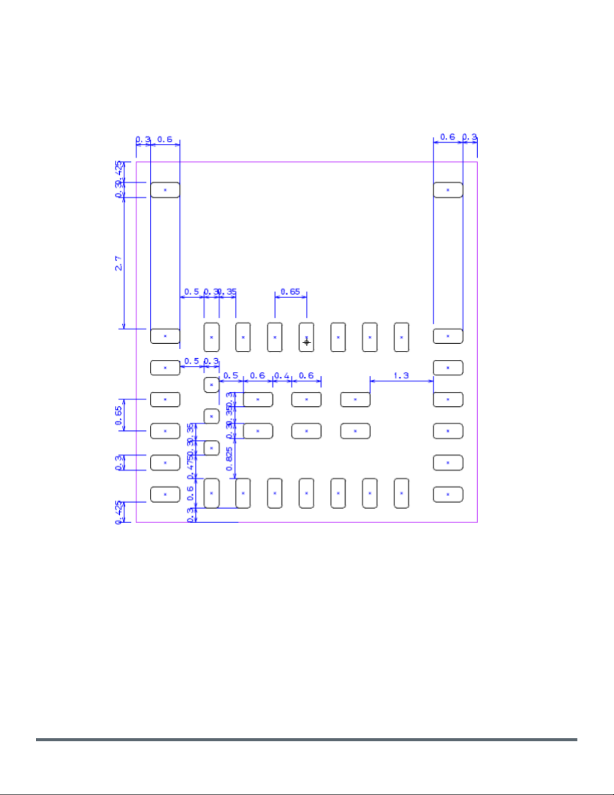
Figure 7.1 Recommended PCB Landing Pattern
Page 15
Copyright © Murata Manufacturing Co., Ltd. All rights reserved. October 2017
MBN52832 Data Sheet, v1.5, 12/02/2020 Page 15 of 34 www.murata.com
7.2 Host PCB Layout Recommendations
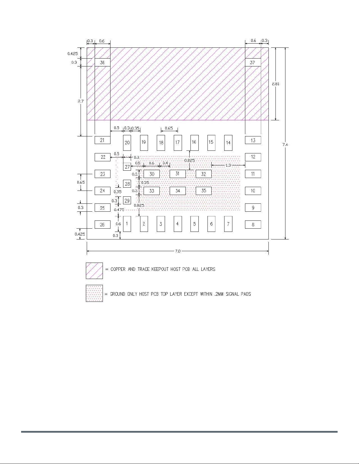
Figure 7.2 Host PCB Layout Recommendation, top view
Page 16
Copyright © Murata Manufacturing Co., Ltd. All rights reserved. October 2017
MBN52832 Data Sheet, v1.5, 12/02/2020 Page 16 of 34 www.murata.com
7.3 Layout Guidance for Using Internal PCB Antenna
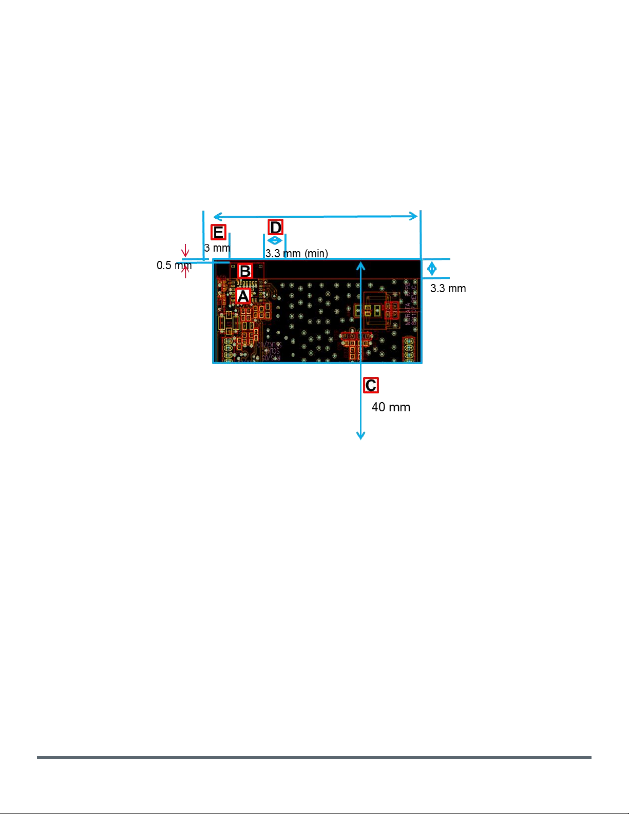
The MBN52832 module is certified with an internal PCB antenna physically located on the module. For optimum EIRP
(Effectively Isotropically Radiated Power) when use the on-board antenna, please follow the following recommendations in
the customer host circuit board design.
A. The module is recommended is be placed on top left corner of the host circuit board.
B. Around the antenna area, all layers of the customer circuit board should be free of any metal objects. Specifically,
there should be no ground plane, traces or metal shield case
C. Host circuit PCB length is longer than 40mm to get optimal performance by using ground plane.
D. Right side of antenna area also should be free of grounds.
E. Metal and plastic materials should be away from the module. (more than 3mm)
Figure 7.3 Layout Guide for Antenna Performance (1)
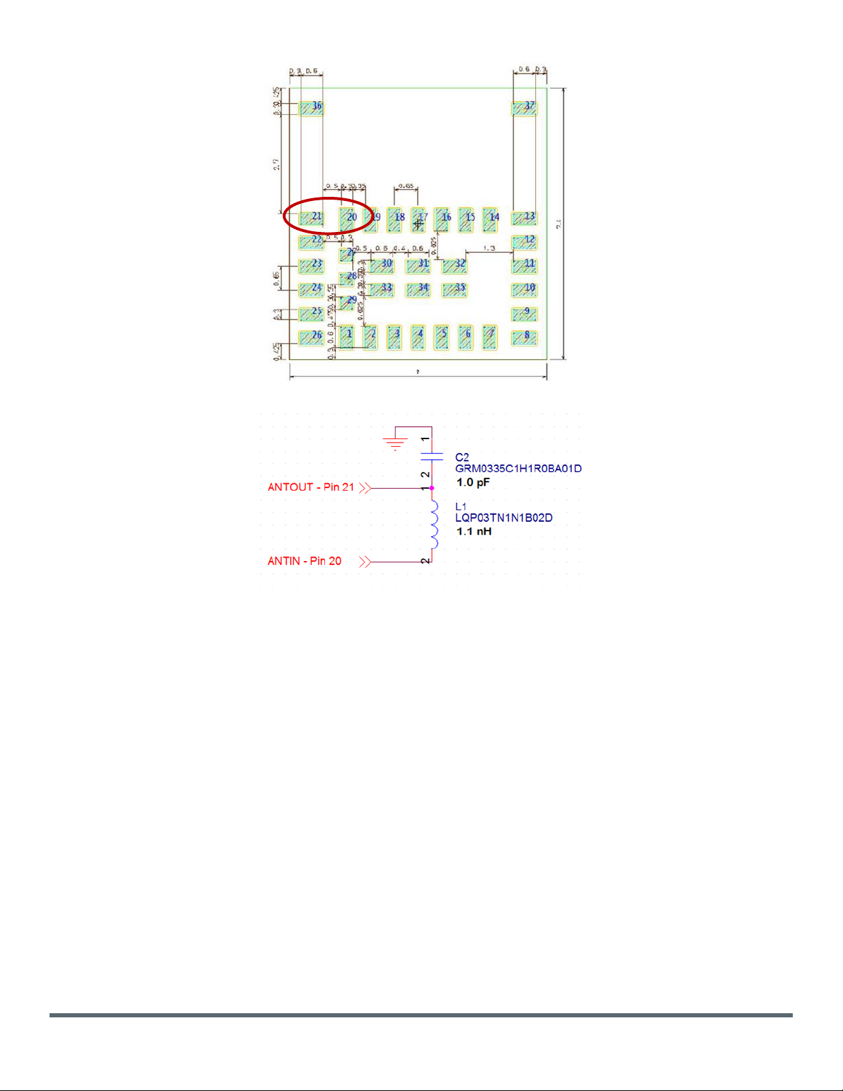
F. To use this internal antenna, the integrator must provide a simple two-component matching circuit between pins 20
and 21 of the module. This circuit will connect the RF I/O of the module directly to the PCB antenna. The picture
below shows the location of pins 20 and 21.
Page 17
Copyright © Murata Manufacturing Co., Ltd. All rights reserved. October 2017
MBN52832 Data Sheet, v1.5, 12/02/2020 Page 17 of 34 www.murata.com
Figure 7.4 Layout Guide for Antenna Performance (2)
The Integrator must place the matching circuit shown below between Pins 20 and 21 of the Module to duplicate the
structure used during FCC/IC testing of the MBN52832. Use the exact PNs provided for L1 and C2 to meet regulatory
requirements.
On the integrator’s support board, place L1 between Pin 20 and Pin 21 of the Module. Place C2 adjacent to Pin 21. The
other side of C2 should be attached to RF Ground.
Any technical implementation questions regarding the layout or design of this circuit should be directed to Murata module
technical support.
7.4 Layout Guidance for Microstrip Design And External Antenna
The MBN52832 module is certified with an internal PCB antenna and two external antennas; a 7 dBi omni antenna and a 6
dBi patch antenna.
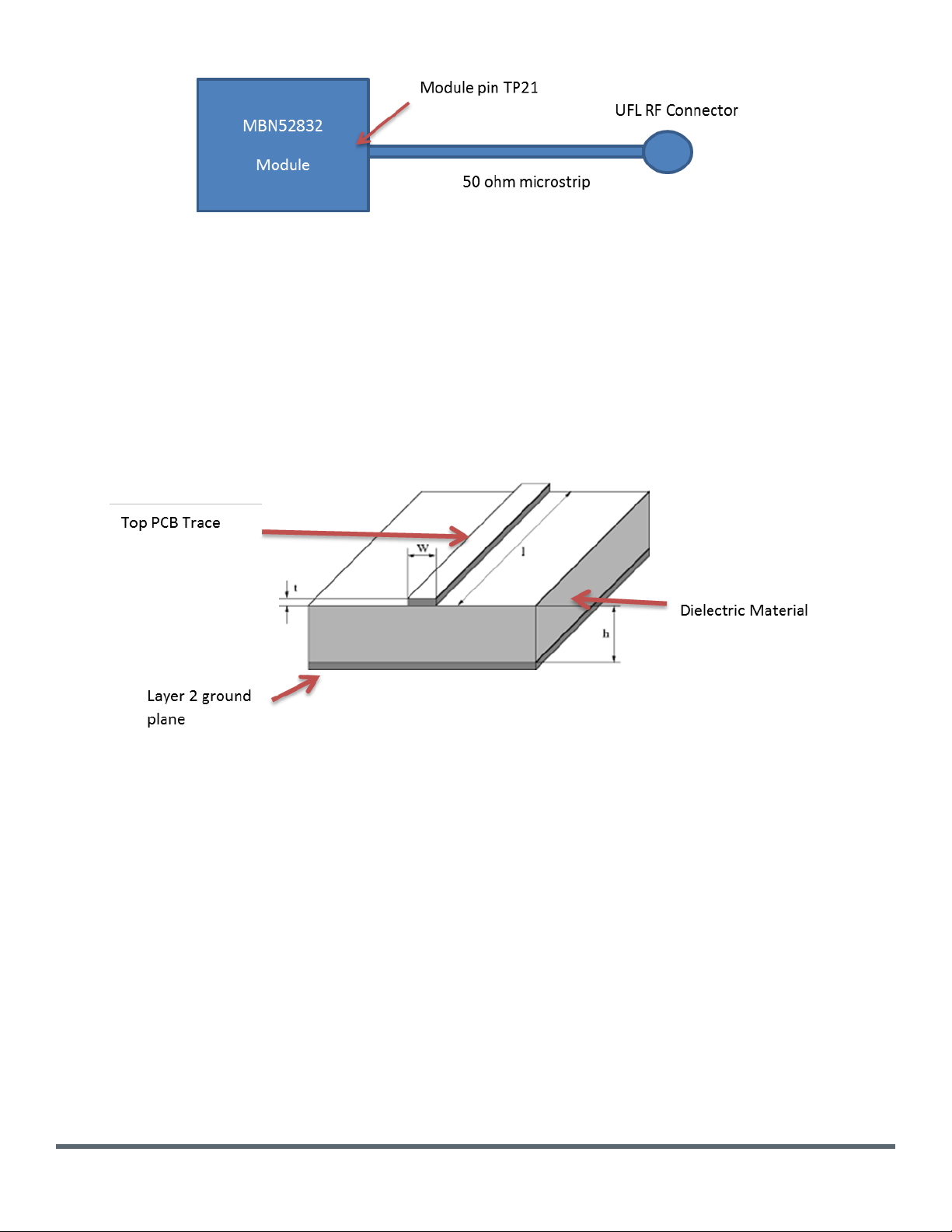
Either patch or omni antenna should be connected to the MBN module using 50 ohm microstrip and a U.FL RF connector
as shown below. This microstrip and U.FL connector are placed on the customer’s PCB and are external to the MBN
module. The patch or omni antenna is then connected to this UFL Connector via a 50 ohm RF adapter cable.
Page 18
Copyright © Murata Manufacturing Co., Ltd. All rights reserved. October 2017
MBN52832 Data Sheet, v1.5, 12/02/2020 Page 18 of 34 www.murata.com
Figure 7.5 Layout Guide for External Antenna (1)
The design of the 50 ohm microstrip on the customer’s PCB is crucially important. Compliant operation of the MBN is
dependent on proper construction of this 50 ohm line and the following guidelines must be followed to ensure legal operation
of the product.
The diagram below shows the required microstrip structure to be routed between module pin TP21 and the UFL connector.
The top PCB trace carries the RF energy from module to UFL connector. The Layer2 ground plane provides a return path
for the circuit. The Dielectric material (along with the dimensions of the microstrip structures) determines the characteristic
impedance of the microstrip transmission line.
Figure 7.6 Layout Guide for External Antenna (2)
Note the representative dimensions shown in the drawing above. It is imperative that the module customer (the integrator)
use the exact dimensions we recommend to ensure a 50-ohm impedance for this transmission line.
The following dimensions and/or ratios should be used to set the microstrip impedance to 50 ohms.
Dielectric (PCB) Material – We recommend standard FR-4 PCB material. Other dielectrics will work but will require
recalculation of microstrip dimensions. The following guidance is predicated on the use of FR-4 Dielectric. If FR-4 is not
used for PCB material, please contact Murata Electronics at (678) 684-2009 to determine new dimensions for microstrip
structure.
H (Dielectric Height) – this is the thickness of dielectric between the trace layer (layer 1) and the ground plane on layer 2.
Note that layer 2 must be electrical ground. We recommend a dielectric thickness of 8-15 mils. This range provides the
customer with some flexibility in board construction.
t (trace thickness) – Microstrip impedance is not severely affected by the thickness dimension. Standard 1oz or 2oz copper
deposition is recommended. Equivalent thickness is 1-2 mils.
W (trace width) – this is the crucial dimension. This width must be set correctly to obtain the desired 50 ohms impedance.
When using FR-4 dielectric, the width (W) of the microstrip trace should be set to:
Page 19

Copyright © Murata Manufacturing Co., Ltd. All rights reserved. October 2017
MBN52832 Data Sheet, v1.5, 12/02/2020 Page 19 of 34 www.murata.com
W = H * 1.8
Where W is microstrip trace width and H is Dielectric height. Note that both values must be measured in identical units (mils
or mm)
Example:
H = 12 mils, W = 12 * 1.8 = 21.6 mils
H = 0.4 mm W = 0.4 * 1.8 = 0.72 mm
l (trace length) – the impedance of the microstrip line is not dependent on its length. However, regulatory and performance
limitations practically determine the actual length to be used by the customer (integrator). The length of this microstrip line
must be longer than 7 mm to mimic the length used during FCC/IC certification of the MBN52832 module. Lengths longer
than 7 mm are acceptable although additional signal loss will occur as a result. Given these restrictions, Murata recommends
microstrip trace lengths between 7 mm and 25 mm.
In any event, the microstrip line must operate over the same Dielectric-Ground Plane configuration shown above to act as
a 50 ohm transmission line. Do not run the microstrip trace through sections of PCB that do not have the Dielectric-Ground
plane configuration shown above.
A reliable 50 ohm transmission line will be produced if the above guidance is closely followed. Any deviations from the
guidance above may cause the module to operate in noncompliant manner. Any implementation questions or concerns
should be directed to Murata module technical support. .
Page 20
Copyright © Murata Manufacturing Co., Ltd. All rights reserved. October 2017
MBN52832 Data Sheet, v1.5, 12/02/2020 Page 20 of 34 www.murata.com
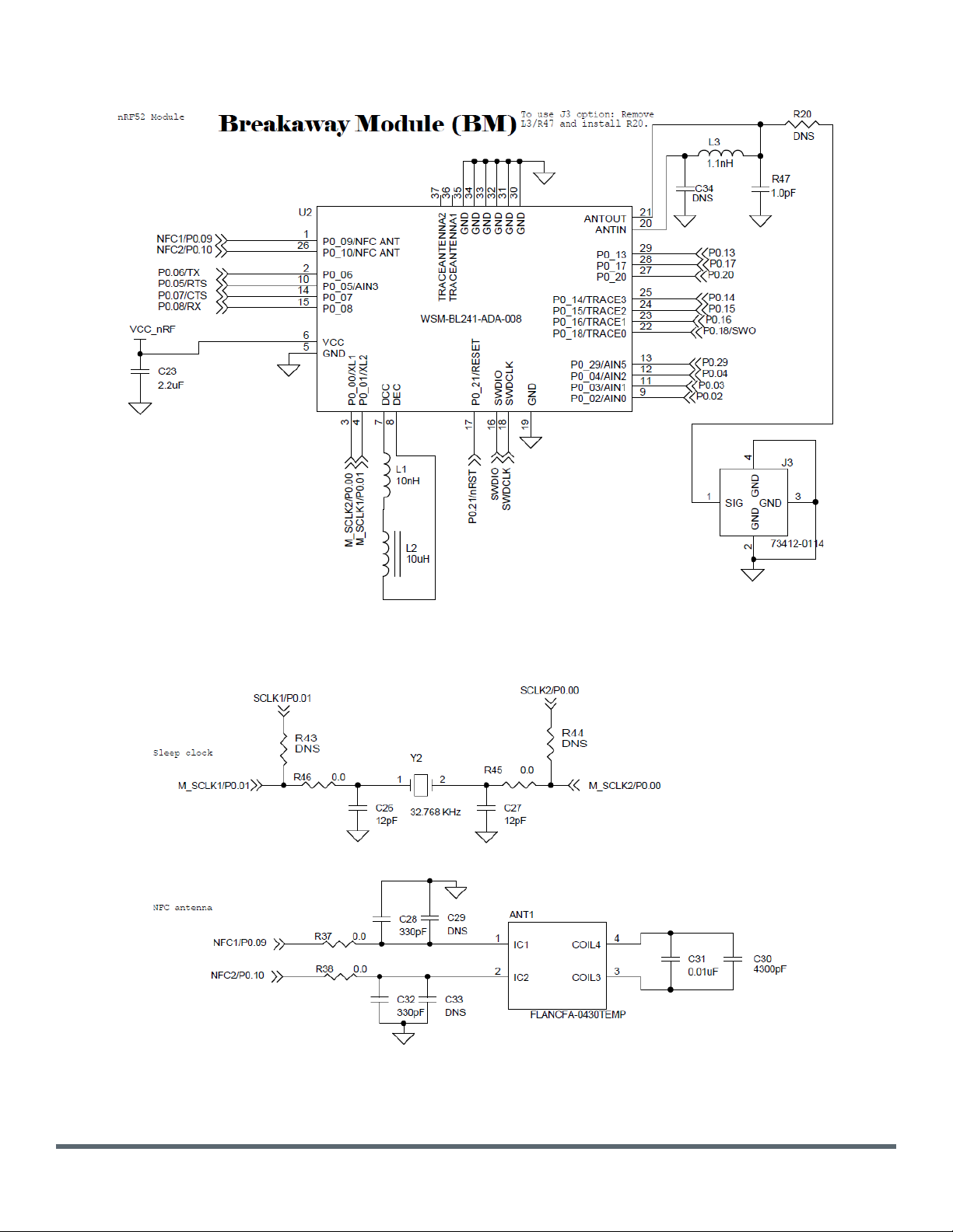
8 Application Reference
Notes:
Option #1: DC/DC converter: as it is
Option #2: LDO: remove L1 and L2
Figure 8.1 Reference Design
Page 21
Copyright © Murata Manufacturing Co., Ltd. All rights reserved. October 2017
MBN52832 Data Sheet, v1.5, 12/02/2020 Page 21 of 34 www.murata.com
9 Assembly Information
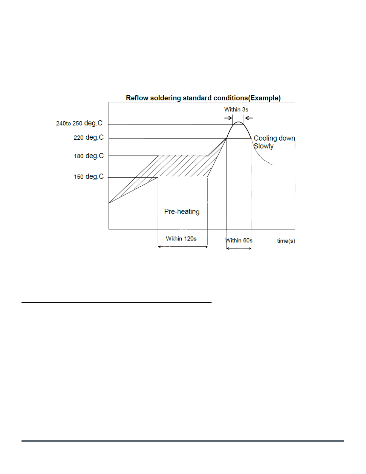
The recommendation conditions of soldering are as in the following figure.
When products are immersed in solvent after mounting, pay special attention to maintain the temperature difference within
100 °C. Soldering must be carried out by the above mentioned conditions to prevent products from damage. Set up the
highest temperature of reflow within 260 °C. Contact Murata before use if concerning other soldering conditions.
Reflow soldering standard conditions
Figure 9.1 Reflow Profile
Please use the reflow within 2 times.
Use rosin type flux or weakly active flux with a chlorine content of 0.2 wt % or less.
Since this Product is Moisture Sensitive, any cleaning is NOT permitted.
Page 22
Copyright © Murata Manufacturing Co., Ltd. All rights reserved. October 2017
MBN52832 Data Sheet, v1.5, 12/02/2020 Page 22 of 34 www.murata.com
10 Packaging and Marking Information
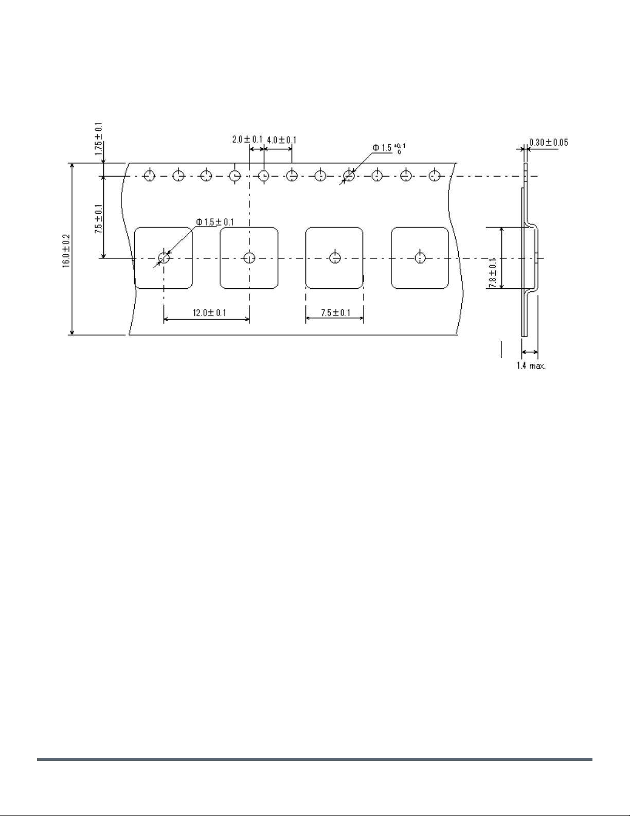
10.1 Dimensions of Tape (Plastic tape)
Figure 10.1 Tape Dimensions (Unit in mm)
Page 23
Copyright © Murata Manufacturing Co., Ltd. All rights reserved. October 2017
MBN52832 Data Sheet, v1.5, 12/02/2020 Page 23 of 34 www.murata.com
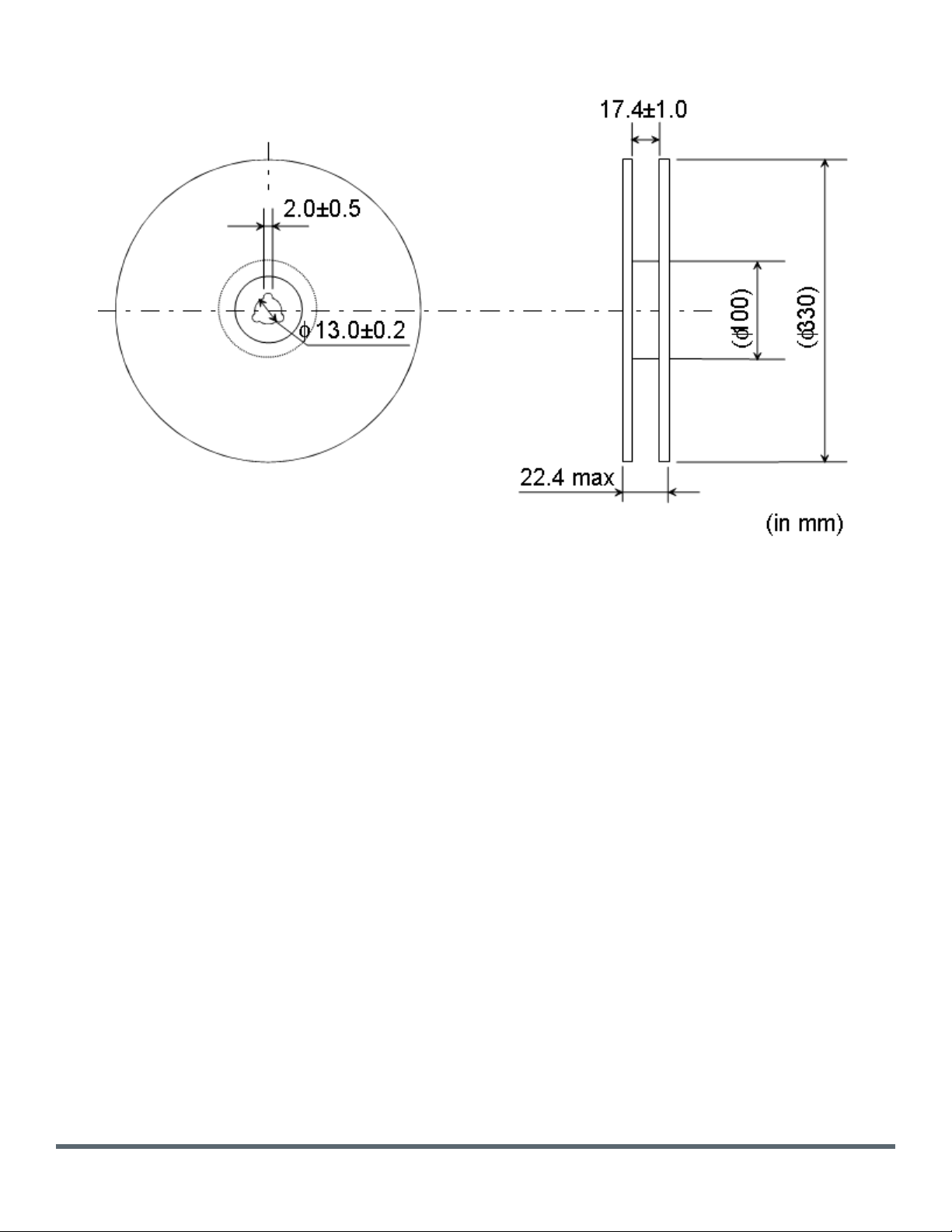
10.2 Dimensions of Reel
Figure 10.2 Reel Dimensions (Unit: mm)
Page 24
Copyright © Murata Manufacturing Co., Ltd. All rights reserved. October 2017
MBN52832 Data Sheet, v1.5, 12/02/2020 Page 24 of 34 www.murata.com
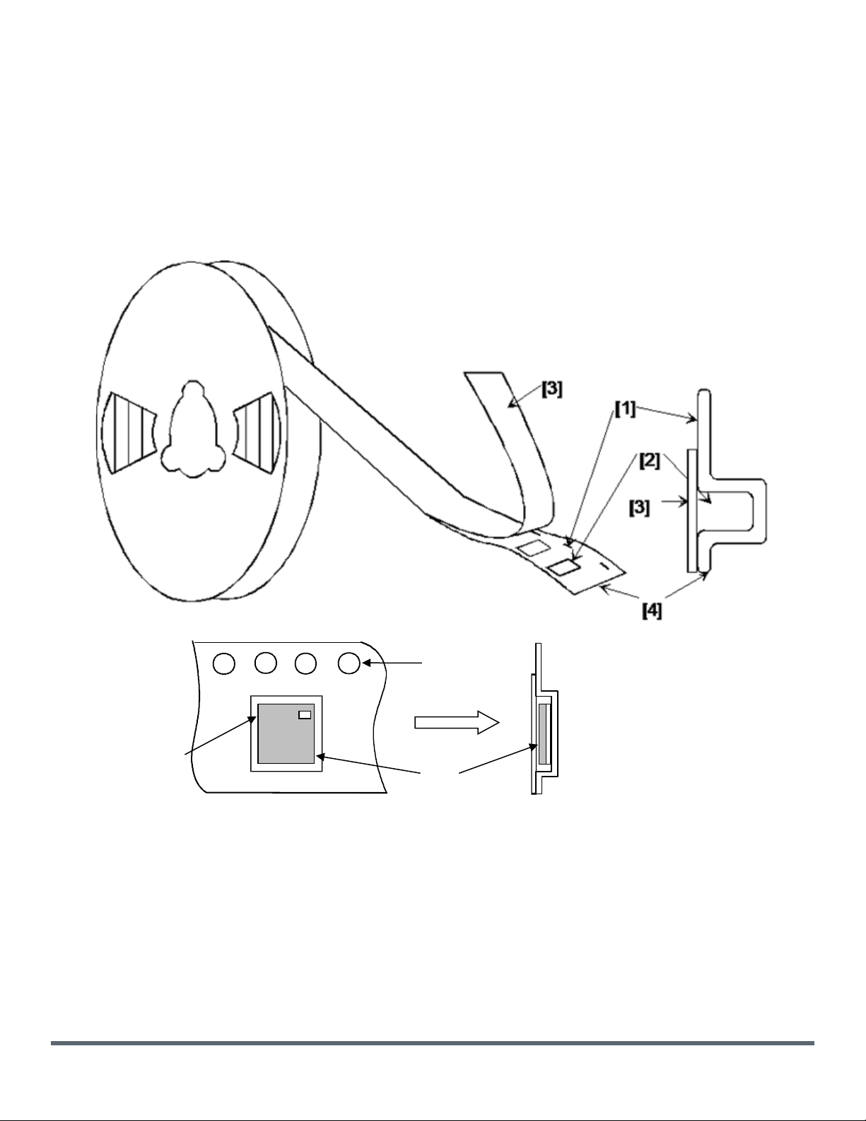
10.3 Taping Diagrams
[1] Feeding Hole : As specified in (1)
[2] Hole for chip : As specified in (1)
[3] Cover tape : 62 um in thickness
[4] Base tape : As specified in (1)
Figure 10.3 Tape Diagram
Feeding Hole
Chip
Feeding Direction
Pin 1 Marking
Page 25
Copyright © Murata Manufacturing Co., Ltd. All rights reserved. October 2017
MBN52832 Data Sheet, v1.5, 12/02/2020 Page 25 of 34 www.murata.com
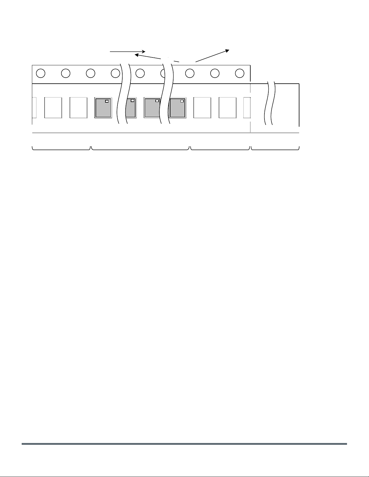
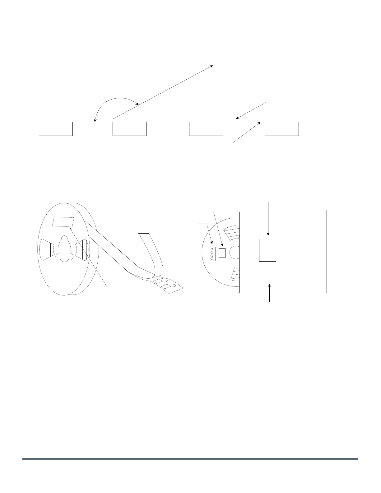
10.4 Leader and Tail tape
Figure 10.4 Tape Leader and Tail
The tape for chips are wound clockwise, the feeding holes to the right side as the tape is pulled toward the user.
The cover tape and base tape are not adhered at none components area for 250 mm min.
Tear off strength against pulling of cover tape: 5 N min.
Packaging unit: 1000 pcs./ reel
Material:
- Base tape : Plastic
- Reel : Plastic
- Cover tape, cavity tape and reel are made the anti-static processing.
Tail tape
(No components)
40 to 200mm
Components
No components
150mm min.
Leader tape
(Cover tape
alone)
250mm min.
Feeding
Page 26
Copyright © Murata Manufacturing Co., Ltd. All rights reserved. October 2017
MBN52832 Data Sheet, v1.5, 12/02/2020 Page 26 of 34 www.murata.com
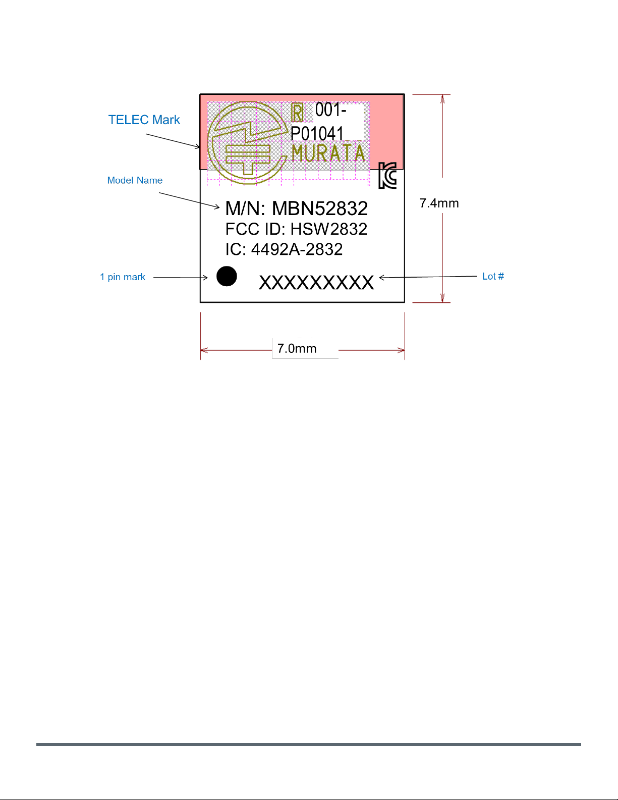
10.5 Peeling Force
1.3 N max. in the direction of peeling as shown below.
Figure 10.5 Peeling Force Diagram
10.6 PACKAGE (Humidity proof Packaging)
Figure 10.6 Packaging Diagram
Tape and reel must be sealed with the anti-humidity plastic bag. The bag contains the desiccant and the humidity
indicator.
165 to 180 °
1.3 N max.
Base tape
Cover tape
湿度
イ ン ジケ-タ
乾燥剤
表示ラ べル
防湿梱包袋
表示ラ ベル
Label
Label
Desiccant
Humidity
Indicator
Anti-humidity
Plastic Bag
Page 27
Copyright © Murata Manufacturing Co., Ltd. All rights reserved. October 2017
MBN52832 Data Sheet, v1.5, 12/02/2020 Page 27 of 34 www.murata.com
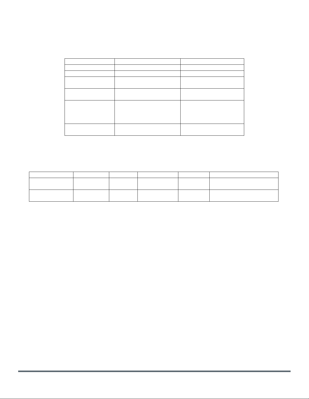
10.7 Module Marking Information
Figure 10.7 shows the module marking. Dimensions are nominal, not absolute.
Figure 10.7 Module Marking Diagram
10.8 Moisture Sensitivity Level
The MBN52832 is planned to be qualified to moisture sensitivity level 3 in accordance with JEDEC J-STD-020.
Page 28
Copyright © Murata Manufacturing Co., Ltd. All rights reserved. October 2017
MBN52832 Data Sheet, v1.5, 12/02/2020 Page 28 of 34 www.murata.com
11 Regulatory Information
The table below shows the regulatory compliance status of the MBN52832 module.
Table 11.1 Regulatory Standards Conformance
Regulatory Body
Standard
Certificate ID
FCC
Part 15
HSW2832
IC
RSS-210
4492A-2832
ETSI
EN300 328, Ver. 2.1.1
ETSI EN301.489 - 17
Compliant
TELEC
Article 38-24 Paragraph 1
of the Radio Law
001-P01041
KC
Non-license based
wireless device technical
standard (MSIT notice
2019-105)
R-C-VPY-MBN52832
BT SIG
BT 5.0
Declaration ID: D036210
QDID: 97989
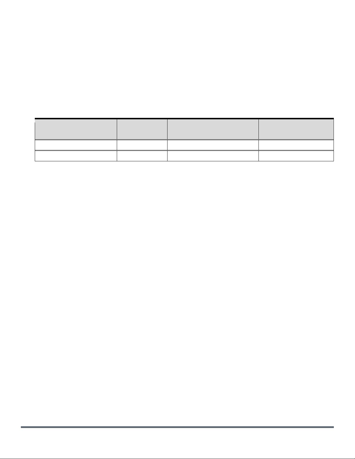
MBN52832 also has been certified with following external antennae (see table below).
Table 11.2 External Antenna to comply with FCC and IC
Part Number
Vendor
Gain (dBi)
Type
Connector
Remarks
S2406PL
Cushcraft
6.0
Patch
U.FL
Necessary for FCC/IC
compliance only.
HG2407RD-RSP
L-Comm
7.0
Dipole
U.FL
Necessary for FCC/IC
compliance only.
To be compliant with RED Directive while using MBN52832 module with external antenna, the total EIRP including the
antenna gain should be less than or equal to 10dBm.
11.1 FCC Notice (USA)
Warning: Changes or modifications to this device not expressly approved by Murata could void the user’s authority to
operate the equipment.
This device complies with Part 15 of the FCC rules. Operation is subject to the following two conditions: (1) this device may
not cause harmful interference, and (2) this device must accept any interference received, including interference that may
cause undesired operation.
The FCC requires the OEM to be notified that any changes or modifications not expressly approved by Murata may void
the user’s authority to operate the equipment. While an application of the MBN52832 module in a product is not required to
obtain a new FCC authorization for the module, this does not preclude the possibility that some other form of authorization
or testing may be required for that end product.
This device using the integrated antenna has been tested to comply with FCC CFR Part 15. The device meets the
requirements for modular transmitter approval as detailed in the FCC 47 CFR 15.212.
This equipment has been tested and found to comply with the limits for a Class B digital device, pursuant to Part 15 of the
FCC Rules. These limits are designed to provide reasonable protection against harmful interference in a residential
installation. This equipment generates uses and can radiate radio frequency energy and, if not installed and used in
accordance with the instructions, may cause harmful interference to radio communications. However, there is no guarantee
that interference will not occur in a particular installation. If this equipment does cause harmful interference to radio or
Page 29

Copyright © Murata Manufacturing Co., Ltd. All rights reserved. October 2017
MBN52832 Data Sheet, v1.5, 12/02/2020 Page 29 of 34 www.murata.com
television reception, which can be determined by turning the equipment off and on, the user is encouraged to try to correct
the interference by one or more of the following measures:
• Reorient or relocate the receiving antenna.
• Increase the separation between the equipment and receiver.
• Connect the equipment into an outlet on a circuit different from that to which the receiver.
• Is connected.
• Consult the dealer or an experienced radio/TV technician for help.
11.2 FCC Labeling Requirements
When integrating the MBN52832 into a product the FCC labeling requirements must be met. This includes a clearly visible
label on the outside of the finished product specifying the MBN52832 FCC identifier (FCC ID: HSW2832) as well as the
notice above. The exterior label can use wording such as “Contains Transmitter Module FCC ID: HSW2832” or “Contains
FCC ID: HSW2832” although any similar wording that expresses the same meaning may be used.
11.3 IC Notice (Canada)
The term “IC” before the certification/registration number only signifies that the Industry Canada technical specifications
were met.
Le terme “IC” devant le numéro de certification /d’enregistrement signifie seulement que les spécifications techniques
Industrie Canada ont été respectées.
This device complies with Industry Canada license-exempt RSS standard(s). Operation is subject to
The following two conditions: (1) this device may not cause interference, and (2) this device must accept any interference,
including interference that may cause undesired operation of the device.
Cet appareil est conforme avec Industrie Canada RSS standard exempts de licence (s). Son utilisation est soumise à Les
deux conditions suivantes: (1) cet appareil ne peut pas provoquer d'interférences et (2) cet appareil doit accepter Toute
interférence, y compris les interférences qui peuvent causer un mauvais fonctionnement du dispositif.
This device complies with Health Canada’s Safety Code 6 / IC RSS-210. The installer of this device should ensure that RF
radiation is not emitted in excess of the Health Canada’s requirement. Information can be obtained at: http://www.hc-
sc.gc.ca/ewh-semt/pubs/radiation/radio_guide-lignes_direct-eng.php
Cet appareil est conforme avec Santé Canada Code de sécurité 6 / IC RSS-210. Le programme d'installation de cet appareil
doit s'assurer que les rayonnements RF n'est pas émis au-delà de l'exigence de Santé Canada. Les informations peuvent
être obtenues: http://www.hc-sc.gc.ca/ewh-semt/pubs/radiation/radio_guide-lignes_direct-eng.php
This radio transmitter MBN52832 has been approved by Industry Canada to operate with the antenna types listed below
with the maximum permissible gain indicated. Antenna types not included in this list, having a gain greater than the maximum
gain indicated for that type, are strictly prohibited for use with this device.
Le présent émetteur radio (identifier le dispositif par son numéro de certification ou son numéro de modèle s'il fait partie du
matériel de catégorie I) a été approuvé par Industrie Canada pour fonctionner avec les types d'antenne énumérés cidessous et ayant un gain admissible maximal et l'impédance requise pour chaque type d'antenne. Les types d'antenne non
inclus dans cette liste, ou dont le gain est supérieur au gain maximal indiqué, sont strictement interdits pour l'exploitation
de l'émetteur.
Table 11.3 External Antenna to comply with IC
Part Number
Vendor
Gain (dBi)
Type
Connector
Remarks
S2406PL
Cushcraft
6.0
Patch
U.FL
Necessary for FCC/IC
compliance only.
HG2407RD-RSP
L-Comm
7.0
Dipole
U.FL
Necessary for FCC/IC
compliance only.
Page 30

Copyright © Murata Manufacturing Co., Ltd. All rights reserved. October 2017
MBN52832 Data Sheet, v1.5, 12/02/2020 Page 30 of 34 www.murata.com
11.4 IC Labeling Requirements
The host device should be properly labeled to identify the module within the host device. The Industry Canada certification
label of a module shall be clearly visible at all times when installed in the host device, otherwise the host device must be
labeled to display the Industry Canada certification number of the module, preceded by the words “Contains transmitter
module”, or the word “Contains”, or similar wording expressing the same meaning, as follows:
Contains transmitter module IC: 4492A-2832, where 4492A-2832 is the module’s certification number.
11.5 ESTI compliance (Europe)
This device has been tested for use in the European Union. Both MBN52832 comply with the following regulation test.
ETSI EN300 328, Ver. 2.1.1
ETSI EN301.489 - 17
If this device is used in a product, the OEM has responsibility to verify compliance of the final product to the EU standards.
A Declaration of Conformity must be issued and kept on file as described in Annex II of the Radio and Telecommunications
Terminal Equipment Directive.
11.6 RF Exposure
11.6.1 Using on-board PCB antenna
This equipment complies with radiation exposure limits set forth for an uncontrolled environment. This equipment is in
direct contact with the body of the user under normal operating conditions. This transmitter must not be co-located or
operating in conjunction with any other antenna or transmitter.
Cet équipement est conforme aux limites d'exposition aux radiations dans un environnement non contrôlé. Cet
équipement est en contact direct avec le corps de l'utilisateur dans des conditions de fonctionnement normales. Cet
émetteur ne doit pas être co-localisées ou opérant en conjonction avec tout autre antenne ou transmetteur.
11.6.2 Using external antenna
This equipment complies with radiation exposure limits set forth for an uncontrolled environment. This equipment should be
installed and operated with minimum distance 20 cm between the radiator and your body. This transmitter must not be colocated or operating in conjunction with any other antenna or transmitter.
Cet équipement est conforme aux limites d'exposition aux radiations dans un environnement non contrôlé. Cet équipement
doit être installé et utilisé à distance minimum de 20 cm entre le radiateur et votre corps. Cet émetteur ne doit pas être colocalisées ou opérant en conjonction avec tout autre antenne ou transmetteur.
If the module will be used for portable applications, the device must undergo SAR testing.
The following statement must be included as a CAUTION statement in manuals for the products to alert users on FCC RF
exposure compliance:
“WARNING: To satisfy FCC RF exposure requirements for mobile transmitting devices, a separation distance of 20 cm or
more should be maintained between the antenna of this device and persons during operation. To ensure compliance,
operations at closer distances than this are not recommended.”
11.7 KC Certificate Notice
Certification Number: R-C-VPY-MBN52832
Name of the applicant: Murata Manufacturing Co., Ltd.
Name of the equipment name (written in the certification): Specific low power wireless device (wireless device for wireless
data communication system)
Model name: MBN52832
Page 31
Copyright © Murata Manufacturing Co., Ltd. All rights reserved. October 2017
MBN52832 Data Sheet, v1.5, 12/02/2020 Page 31 of 34 www.murata.com
Date of Certification: February 2020
Manufacturer/The country of origin: Murata Manufacturing Co., Ltd./ China
12 RoHS Information
The MBN52832 module is conformed to RoHS requirement.
13 Ordering Information
Product
Model Name
Murata Ordering Part Number
Standard Order
Increment
BLE Module
MBN52832
WSM-BL241-ADA-008
1000 pc
Development Kit
MBN52832DK
WSM-BL241-ADA-008DK
1 pcs
Page 32

Copyright © Murata Manufacturing Co., Ltd. All rights reserved. October 2017
MBN52832 Data Sheet, v1.5, 12/02/2020 Page 32 of 34 www.murata.com
14 Notice
14.1 Storage Conditions
Please use this product within 6month after receipt.
- The product shall be stored without opening the packing under the ambient temperature from 5 to 35deg.C and humidity
from 20 to 70%RH.
(Packing materials, in particular, may be deformed at the temperature over 40deg.C.)
- The product left more than 6months after reception, it needs to be confirmed the solderbility before used.
- The product shall be stored in non-corrosive gas (Cl2, NH3, SO2, Nox, etc.).
- Any excess mechanical shock including, but not limited to, sticking the packing materials by sharp object and dropping
the product, shall not be applied in order not to damage the packing materials.
This product is applicable to MSL3 (Based on JEDEC Standard J-STD-020)
- After the packing opened, the product shall be stored at <30deg.C / <60%RH and the product shall be used within
168hours.
- When the color of the indicator in the packing changed, the product shall be baked before soldering.
Baking condition: 125+5/-0deg.C, 24hours, 1time
The products shall be baked on the heat-resistant tray because the material (Base Tape, Reel Tape and Cover Tape) are
not heat-resistant.
14.2 Handling Conditions
Be careful in handling or transporting products because excessive stress or mechanical shock may break products.
Handle with care if products may have cracks or damages on their terminals, the characteristics of products may change.
Do not touch products with bear hands that may result in poor solder ability and destroy by static electrical charge.
14.3 Standard PCB Design (Land Pattern and Dimensions)
All the ground terminals should be connected to the ground patterns. Furthermore, the ground pattern should be provided
between IN and OUT terminals. Please refer to the specifications for the standard land dimensions.
The recommended land pattern and dimensions is as Murata's standard. The characteristics of products may vary
depending on the pattern drawing method, grounding method, land dimensions, land forming method of the NC terminals
and the PCB material and thickness. Therefore, be sure to verify the characteristics in the actual set. If use non-standard
lands, contact Murata beforehand.
14.4 Notice for Chip Placer
When placing products on the PCB, products may be stressed and broken by uneven forces from a worn-out chucking
locating claw or a suction nozzle. To prevent products from damages, be sure to follow the specifications for the
maintenance of the chip placer being used. For the positioning of products on the PCB, be aware that mechanical
chucking may damage products.
14.5 Operational Environment Conditions
Page 33

Copyright © Murata Manufacturing Co., Ltd. All rights reserved. October 2017
MBN52832 Data Sheet, v1.5, 12/02/2020 Page 33 of 34 www.murata.com
Products are designed to work for electronic products under normal environmental conditions (ambient temperature,
humidity and pressure). Therefore, products have no problems to be used under the similar conditions to the abovementioned. However, if products are used under the following circumstances, it may damage products and leakage of
electricity and abnormal temperature may occur.
- In an atmosphere containing corrosive gas ( Cl2, NH3, SOx, NOx etc.).
- In an atmosphere containing combustible and volatile gases.
- Dusty place.
- Direct sunlight place.
- Water splashing place.
- Humid place where water condenses.
- Freezing place.
If there are possibilities for products to be used under the preceding clause, consult with Murata before actual use.
As it might be a cause of degradation or destruction to apply static electricity to products, do not apply static electricity or
excessive voltage while assembling and measuring.
14.6 Input Power Capacity
Products shall be used in the input power capacity as specified in this specification.
Inform Murata beforehand, in case that the components are used beyond such input power capacity range.
Page 34

Copyright © Murata Manufacturing Co., Ltd. All rights reserved. October 2017
MBN52832 Data Sheet, v1.5, 12/02/2020 Page 34 of 34 www.murata.com
15 PRECONDITIONS TO USE MURATA PRODUCTS
PLEASE READ THIS NOTICE BEFORE USING OUR PRODUCTS.
Please make sure that your product has been evaluated and confirmed from the aspect of the fitness for the specifications
of our product when our product is mounted to your product.
All the items and parameters in this product specification/datasheet/catalog have been prescribed on the premise that our
product is used for the purpose, under the condition and in the environment specified in this specification. You are requested
not to use our product deviating from the condition and the environment specified in this specification.
Please note that the only warranty that we provide regarding the products is its conformance to the specifications provided
herein. Accordingly, we shall not be responsible for any defects in products or equipment incorporating such products, which
are caused under the conditions other than those specified in this specification.
WE HEREBY DISCLAIMS ALL OTHER WARRANTIES REGARDING THE PRODUCTS, EXPRESS OR IMPLIED,
INCLUDING WITHOUT LIMITATION ANY WARRANTY OF FITNESS FOR A PARTICULAR PURPOSE, THAT THEY ARE
DEFECT-FREE, OR AGAINST INFRINGEMENT OF INTELLECTUAL PROPERTY RIGHTS.
The product shall not be used in any application listed below which requires especially high reliability for the prevention of
such defect as may directly cause damage to the third party's life, body or property. You acknowledge and agree that, if you
use our products in such applications, we will not be responsible for any failure to meet such requirements. Furthermore,
YOU AGREE TO INDEMNIFY AND DEFEND US AND OUR AFFILIATES AGAINST ALL CLAIMS, DAMAGES, COSTS,
AND EXPENSES THAT MAY BE INCURRED, INCLUDING WITHOUT LIMITATION, ATTORNEY FEES AND COSTS, DUE
TO THE USE OF OUR PRODUCTS IN SUCH APPLICATIONS.
- Aircraft equipment. - Aerospace equipment - Undersea equipment.
- Power plant control equipment - Medical equipment.
- Transportation equipment (vehicles, trains, ships, elevator, etc.).
- Traffic signal equipment. - Disaster prevention / crime prevention equipment.
-Burning / explosion control equipment
- Application of similar complexity and/ or reliability requirements to the applications listed in the above.
We expressly prohibit you from analyzing, breaking, reverse-engineering, remodeling altering, and reproducing our product.
Our product cannot be used for the product which is prohibited from being manufactured, used, and sold by the regulations
and laws in the world.
We do not warrant or represent that any license, either express or implied, is granted under any our patent right, copyright,
mask work right, or our other intellectual property right relating to any combination, machine, or process in which our
products or services are used. Information provided by us regarding third-party products or services does not constitute a
license from us to use such products or services or a warranty or endorsement thereof. Use of such information may require
a license from a third party under the patents or other intellectual property of the third party, or a license from us under our
patents or other intellectual property.
Please do not use our products, our technical information and other data provided by us for the purpose of developing of
mass-destruction weapons and the purpose of military use.
Moreover, you must comply with "foreign exchange and foreign trade law", the "U.S. export administration regulations", etc.
Please note that we may discontinue the manufacture of our products, due to reasons such as end of supply of materials
and/or components from our suppliers.
By signing on specification sheet or approval sheet, you acknowledge that you are the legal representative for your company
and that you understand and accept the validity of the contents herein. When you are not able to return the signed version
of specification sheet or approval sheet within 30 days from receiving date of specification sheet or approval sheet, it shall
be deemed to be your consent on the content of specification sheet or approval sheet. Customer acknowledges that
engineering samples may deviate from specifications and may contain defects due to their development status. We reject
any liability or product warranty for engineering samples. In particular we disclaim liability for damages caused by
- the use of the engineering sample other than for evaluation purposes, particularly the installation or integration in the
product to be sold by you,
-deviation or lapse in function of engineering sample,
-improper use of engineering samples.
We disclaim any liability for consequential and incidental damages.
If you can’t agree the above contents, you should inquire our sales.
 Loading...