

Page 1
>
RPR 583
TM1212 Issue 1 Page (i)
TECHNICAL MANUAL
for
RADIO PAGING RECEIVER
MODEL RPR 583
Printed and Published in England
Page 2

RPR 583
TM1212 Issue 1Page (ii)
COMPANY LIABILITY
The information in this manual has been carefully compiled and checked for technical
accuracy. Multitone Electronics plc accept no liability for inaccuracies or errors. In line with
the company policy of technical advancement, the information within this document may be
changed. The user should ensure that the correct issue of the document is used. Comments
or correspondence regarding this manual should be addressed to:
Multitone Electronics plc
Technical Publications
Beggarwood Lane
Basingstoke
Hampshire
RG23 7LL
England
ISSUE DATE
1 July 1999
© 1999 Multitone Electronics plc
Page 3

RPR 583
TM1212 Issue 1 Page (iii)
CONTENTS
Page (i) Title Page
Page (ii) Company Liability
Page (iii) Contents
Page (iv) Effective Page List
Page (v) Safety Summary
Warning
Caution
Section 1 Introduction and Specification
Section 2 Operating Instructions
Section 3 Technical Description
Section 4 Installation & Commissioning
Section 5 Servicing
Section 6 Spare Parts List
Section 7 Diagrams
Page 4

RPR 583
TM1212 Issue 1Page (iv)
EFFECTIVE PAGE LIST
Page No. Issue Page No. Issue Page No. Issue Page No. Issue
(I) 1 2-11 1
(ii) 1 2-12 1
(iii) 1 2-13 1
(iv) 1 2-14 1
(v) 1 2-15 1
(vi) 1 2-16 1
1-1 1 2-17 1
1-2 1 2-18 1
1-3 1 3-1 1
1-4 1 3-2 1
1-5 1 3-3 1
1-6 1 3-4 1
2-1 1 3-5 1
2-2 1 3-6 1
2-3 1 3-7 1
2-4 1 3-8 1
2-5 1 3-9 1
2-6 1 3-10 1
2-7 1 4-1 1
2-8 1 4-2 1
2-9 1 5-1 1
2-10 1 5-2 1
5-3 1
5-4 1
5-5 1
5-6 1
5-7 1
5-8 1
5-9 1
5-10 1
5-11 1
5-12 1
5-13 1
5-14 1
5-15 1
5-16 1
5-17 1
5-18 1
5-19 1
5-20 1
5-21 1
5-22 1
5-23 1
5-24 1
5-25 1
5-26 1
5-27 1
5-28 1
6-1 1
6-2 1
6-3 1
6-4 1
6-5 1
6-6 1
6-7 1
6-8 1
6-9 1
6-10 1
7-1 1
7-2 1
7-3/4 1
7-5/6 1
7-7/8 1
7-9/10 1
7-11/12 1
7-13/14 1
7-15/16 1
7-17/18 1
Page 5
RPR 583
TM1212 Issue 1 Page (v)
THE RECEIVER SHOULD NOT BE CARRIED INTO AREAS WHERE EXPLOSIVE GASES
MAY BE PRESENT.
SAFETY SUMMARY
The following information applies to both operating and servicing personnel. General Warning s
and Cautions will be found throughout the manual, where they apply, which refer to the applicable
part of this summary.
WARNING statements identify conditions or practices that could result in personal injury or loss
of life.
CAUTION statements identify conditions or practices that could result in equipment damage.
WARNING
CAUTION
STATIC SENSITIVE DEVICES ARE USED WITHIN THIS EQUIPMENT. CARE MUST BE
USED TO ENSURE DAMAGE TO THESE DEVICES IS NOT CAUSED BY HIGH LEVELS OF
STATIC ELECTRICITY. SPARE BOARDS OR COMPONENTS SHOULD BE STORED IN
ANTI-STATIC PACKAGING WHEN NOT INSTALLED IN THE EQUIPMENT.
PROTECT THE RECEIVER FROM LIQUIDS, STRONG MAGNETIC FIELDS AND EXTREME
TEMPERATURES. DO NOT LEAVE THE RECEIVER EXPOSED TO STRONG SUNLIGHT.
AREAS SUCH AS WINDOW LEDGES ARE TO BE AVOIDED.
Page 6

RPR 583
TM1212 Issue 1Page (vi)
INTENTIONALLY BLANK
Page 7

RPR 583
TM1212 Issue 1 Page 1 - 1
SECTION 1
INTRODUCTION & SPECIFICATION
CONTENTS: Page
1.1 INTRODUCTION 1 - 2
1.2 FEATURES 1 - 2
1.3 SPECIFICATIONS 1 - 3
1.3.1 Receiver Performance 1 - 3
1.3.2 Power Supply 1 - 4
1.3.3 Code Format 1 - 4
1.3.4 Memory 1 - 4
1.3.5 Displays, Controls and Alerts 1 - 5
1.3.6 Operational Environment 1 - 5
1.3.7 Dimensions 1 - 5
1.3.8 Weight 1 - 5
TABLES:
1.1 Sensitivity Figures 1 - 3
Page 8

RPR 583
TM1212 Issue 1Page 1 - 2
1.1 INTRODUCTION
The Multitone RPR 583 pager is a UHF receiver for On-site applications. The pager
receives alpha-numeric messages sent in Multitone Mk7 digital format.
The front panel of the unit has a Liquid Crystal Display (LCD) to display messages
and other information. The unit has a choice of fonts for the LCD which the operator
can select. The three buttons on the front panel are used to control the functions
of the unit.
If the unit receives a message which has more characters than the display can show,
the excess characters are stored. The front panel buttons are used to transfer the
stored part of the message to the screen as required.
Message alert is provided by an audible beep tone and/or by the unit vibrating. The
front panel buttons are used to select the preferred alert (where this option has been
enabled).
Power for the unit is supplied by a single AAA battery. The unit has the facility to be
used with an ‘absence/charging’ rack. The external contacts provide the interface
for charging the rechargeable battery (where fitted) and for the exchange of data
between the unit and the base station. A door on the rear of the unit gives access
to the battery compartment.
A back-up supply for the unit is available when the battery is changed. The back-up
supply is provided by a large-value capacitor, mounted on the decoder board in the
unit. The capacitor, when fully charged, can maintain data in the unit for more than
5 minutes.
The unit case is a 2-piece plastic moulding secured by two cross-head screws. A
lanyard is supplied with the unit which can be fastened to the case and the attached
clip used to secure the unit to a suitable object e.g. belt, or the holster also supplied.
1.2 FEATURES
C Displays 2 or 4 lines of characters
C Message Store
C Display Illumination
C Date/Time Display
C Selectable Alert - Audible Beep and Vibration
C Alarm
C Timed-off Mode
C Low Battery Warning
C Absence/charging rack connections
Page 9
RPR 583
TM1212 Issue 1 Page 1 - 3
1.3 SPECIFICATIONS
1.3.1 Receiver Performance
Frequency Range: 430 MHZ through 470 MHZ
Frequency Bands:
Band 1: 430.000 MHZ - 434.999 MHZ
Band 2: 435.000 MHZ - 439.999 MHZ
Band 3: 440.000 MHZ - 443.999 MHZ
Band 4: 444.000 MHZ - 446.999 MHZ
Band 5: 447.000 MHZ - 450.999 MHZ
Band 6: 451.000 MHZ - 456.999 MHZ
Band 7: 457.000 MHZ - 462.999 MHZ
Band 8: 463.000 MHZ - 469.999 MHZ
Channel Spacing: 25kHz
Intermediate Frequencies: 45MHz and 455kHz
Crystal Frequencies (except Band 4):
Local Oscillator: Carrier Frequency - 45MHz
3
2nd Oscillator: 44.545MHz Band 4:- 45.455MHz
Sensitivity:
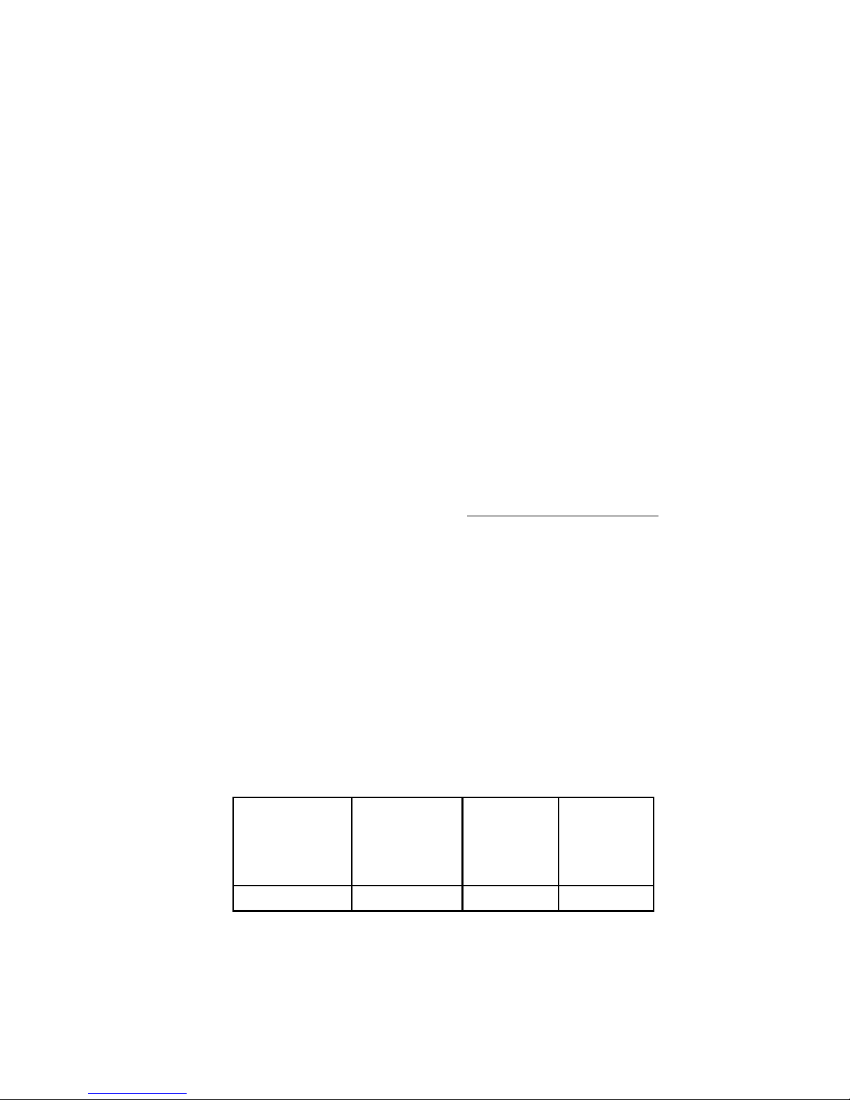
The sensitivity figures quoted in Table 1 assume an ambient temperature in the
range 18 EC through 25 EC. The battery voltage should be above the low battery
trigger point of approximately 1.15 volts. At temperatures between the ambient and
maximum / minimum, performance is at an intermediate value. At temperature
extremes degradation of sensitivity shall not exceed 6dB.
Table 1.1: Sensitivity Figures
MEASUREMENT
MODE
BEST
POSITION,
GUARANTEED
MINIMUM
BEST
POSITION,
TYPICAL
TEM CELL
(dBm),
TYPICAL
On Pole 27 dBµVm 20 dBµVm -105 dBm
-1 -1
Page 10

RPR 583
TM1212 Issue 1Page 1 - 4
NOTE: The following performance figures are typical for an ambient temperature
range of 15 EC through 35 EC.
Adjacent Channel Selectivity: >60 dB
Image Response: >50 dB
Spurious Response: >50 dB
Intermodulation Response: >55 dB
Co-channel Rejection: >-6 dB
1.3.2 Power Supply
Battery Type:
Disposable Alkaline AAA (1.5 Volts Nominal)
Rechargeable Nicad AAA
Typical Battery Life (disposable): 800 hrs
1.3.3 Code Format
The Code Type is Multitone Mk7 digital format
1.3.4 Memory
Capacity: The unit can accept messages to a
maximum of 1024 alpha-numeric
characters. The pager can store a
maximum of 64 read or unread messages
and six archive messages.
Recall: Stored messages can be retrieved in any
order.
Page 11

RPR 583
TM1212 Issue 1 Page 1 - 5
1.3.5 Displays, Controls and Alerts
Liquid Crystal Display: The display shows two or four lines of
characters. The maximum number of
characters in each line depends on the
font selected. The maximum number of
symbols which can be displayed at one
time depends on which symbols are
showing.
Display Illumination: The lamp is selected ON or OFF by using
the front panel controls.
Control Buttons: Three push-buttons on the font panel of
the unit control all the functions of the
pager.
Audible Alert: Various tones which can be selected or
muted by using the front panel controls.
Vibration: The vibration alert can be selected
independently of the audible alert.
1.3.6 Operational Environment
The unit will operate to specification in these limits:
Operating Temperature: -10 EC through +55 EC
Storage Temperature: -20 EC through +60 EC
NOTE: There may be some degradation of display performance below 0 EC.
1.3.7 Dimensions
Width: 75 mm
Height 48 mm
Depth 17 mm
1.3.8 Weight
With battery: 65 g
Page 12

RPR 583
TM1212 Issue 1Page 1 - 6
INTENTIONALLY BLANK
Page 13

RPR 583
TM1212 Issue 1 Page 2 - 1
SECTION 2
OPERATING INSTRUCTIONS
CONTENTS: Page
2.1 CONTROLS AND DISPLAY 2 - 2
2.1.1 Controls 2 - 3
2.1.2 Display 2 - 3
2.1.3 Display On Demand 2 - 3
2.2 OPERATING INSTRUCTIONS 2 - 3
2.2.1 Switching the Unit ON 2 - 3
2.2.2 Setting the Options 2 - 4
2.2.3 Archive 2 - 4
2.2.4 Alarm 2 - 5
2.2.5 Alert (Optional Feature) 2 - 6
2.2.6 Display 2 - 8
2.2.7 Setting the Time and Date and Timed-off Time 2 - 9
2.2.8 Setting the Time and Date 2 - 10
2.2.9 Setting the Timed-off Time 2 - 11
2.2.10 Deleting Messages 2 - 12
2.2.11 Switching the Unit OFF 2 - 13
2.3 RECEIVING AND STORING MESSAGES 2 - 14
2.3.1 Introduction 2 - 14
2.3.2 Receiving a Message 2 - 14
2.3.3 Reviewing Stored Messages 2 - 15
2.3.4 Archiving Messages 2 - 16
2.3.5 Reviewing Information Service Messages 2 - 16
2.3.6 Out of Range (Optional Feature) 2 - 16
2.4 LOW BATTERY 2 - 17
2.4.1 Low Battery Warning (Optional Feature) 2 - 17
2.4.2 Replacing the Battery 2 - 17
2.4.3 Charging Rack 2 - 18
2.5 LANYARD ASSEMBLY 2 - 19
FIGURES:
2.1 Controls and Display 2 - 2
2.2 Main Menu 2 - 4
2.3 Opening the Battery Door 2 - 17
2.4 Lanyard Assembly 2 - 19
Page 14
LCD
CONTROL BUTTONS
TAG11217-1
>
RPR 583
TM1212 Issue1Page 2 - 2
DO NOT TAKE THE PAGER INTO AREAS WHERE EXPLOSIVE GASES MAY BE
PRESENT.
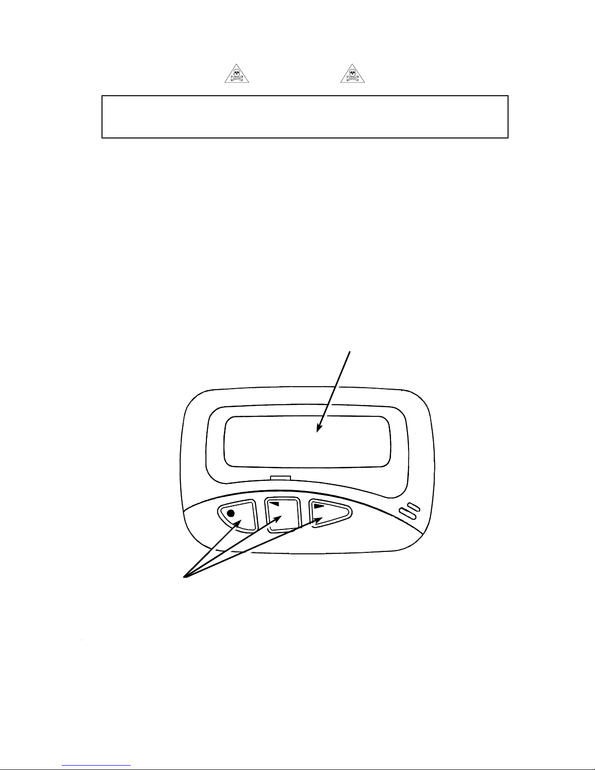
Figure 2.1: Controls and Display
WARNING
CAUTION
PROTECT THE PAGER FROM LIQUIDS, STRONG MAGNETIC FIELDS AND
EXTREME TEMPERATURES. DO NOT LEAVE THE PAGER EXPOSED TO
STRONG SUNLIGHT.
2.1 CONTROLS AND DISPLAY
Refer to Figure 2.1 for the identification and location of the controls and display
associated with the RPR 583.
Page 15

RPR 583
TM1212 Issue 1 Page 2 - 3
2.1.1 Controls
The three push-buttons have these functions:
O> Selects the unit functions
Moves the cursor to the left
Moves the cursor to the right
2.1.2 Display
The Liquid Crystal Display (LCD) shows messages, symbols and other information
associated with the unit. The operator can choose the style of characters shown on
the display from the available list. The display contrast can also be adjusted to suit
the operator’s preference. A lamp is incorporated in the unit to illuminate the display
when required.
2.1.3 Display On Demand
This is a pre-programmable option, which forces the display to “blank” after a pre-
determined time period. At unit switch-on, the screen will display the information as
described in section 2.2.1 and will then switch to the quiescent state, with a blank
screen. This status will remain until either a call is received, one of the user buttons
is depressed, or there is any other change in the status of the pager, such as low
battery alert.
2.2 OPERATING INSTRUCTIONS
2.2.1 Switching the Unit ON
When the battery is installed in the unit, the display shows the time (and the date or
identification, if programmed) on the bottom line and the status symbols on the top
line. The display stays on until the battery is removed or the unit is turned OFF,
unless the unit has been programmed for Display On Demand (see section 2.1.3).
If the unit is turned ‘OFF’ , push and hold the O> button until the Audio and Vibrate
Alerts operate. The display then shows a message for a short time before the time
and symbols show. This is the ‘standby’ screen.
Page 16
ARCHIVE ALERT DISPLAY SET TIME
DELETE
MESSAGES
OFF
ALARM
TAG11350-1
RPR 583
TM1212 Issue1Page 2 - 4
Figure 2.2: Main Menu
2.2.2 Setting the Options
Make sure that the unit is ON and that the display shows the standby screen. Push
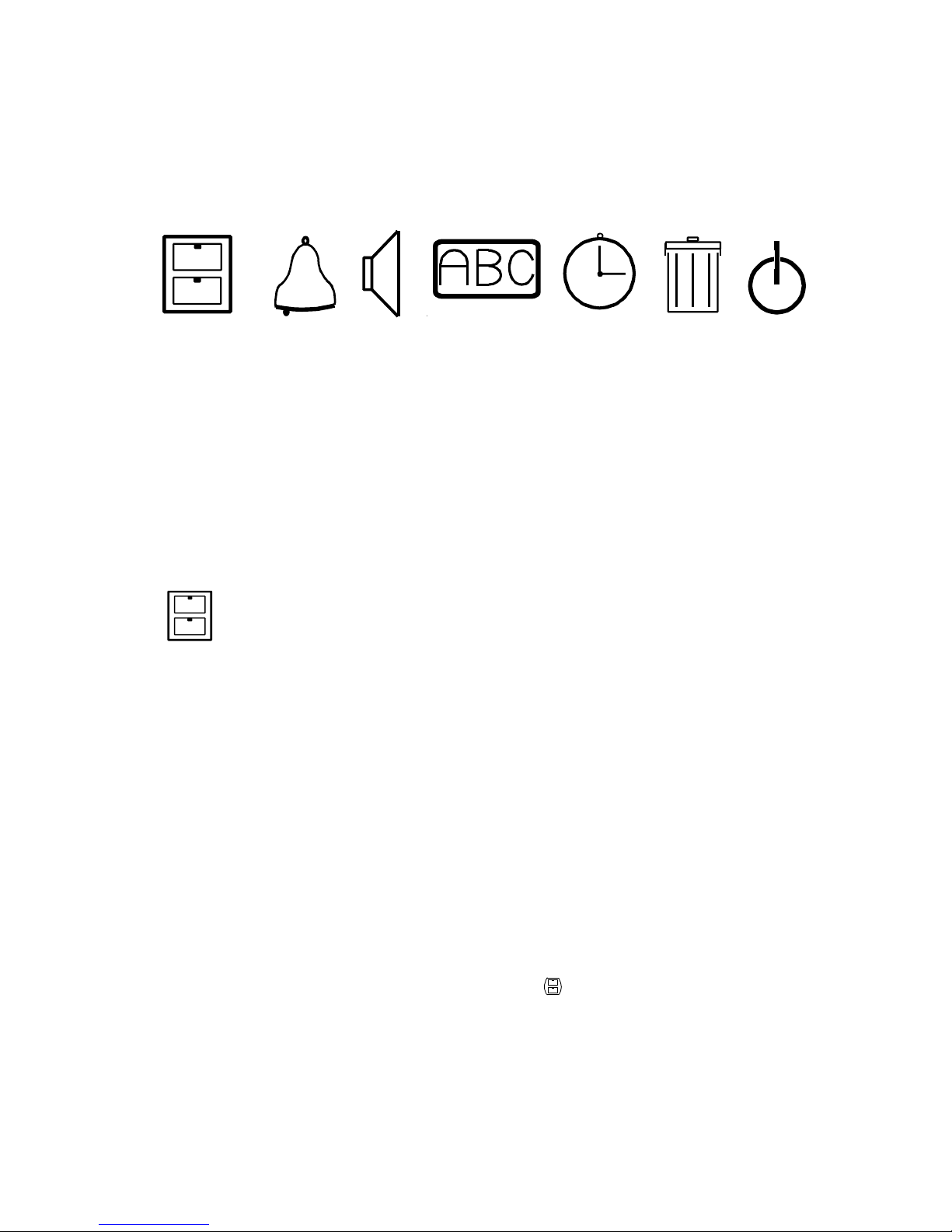
and release the O> button. The display will show the main menu of seven symbols.
These are:
Push the Í or theÌ button to choose the required symbol (the symbol flashes as it
is chosen) then push the O> button to select the function.
Paragraphs 2.2.3 through 2.2.11 give the function and operation of each symbol.
2.2.3 Archive
a) General
This option allows the operator to archive messages and also to view messages
in the archive store.
b) Archiving Messages
Select the required message and view the complete message by pushing the
O> button until the last screen of the message is shown. Push the O> button
once more, then use the Í or theÌ button to choose the archive symbol.
When the archive symbol flashes, push the O> button. The display shows the
archive symbol plus a flashing ?. Push the O> button again to transfer the
message to the archive memory.
If the archive is full, the ‘memory full’ symbol will flash. A message must be
deleted from the archive before the new message can be saved.
Page 17

RPR 583
TM1212 Issue 1 Page 2 - 5
c) Viewing Archived Messages
To view the messages in the archive, select the archive symbol on the main
menu and push the O> button. The display shows the most recent message.
Push the Í or theÌ button to scroll through the messages. If the message is
more than one screen long, push the O> button to display the next screen.
NOTE: If the unit is not programmed to receive information services, push the
Ì button to select the archive directly from the standby screen.
To return to the standby screen, push and hold the O> button for one second
or wait for the unit to time-out and show the standby screen.
2.2.4 Alarm
The alarm can be set to operate once at any time in a twenty four hour period. To
set the alarm:
a) Select the alarm function on the main menu as shown in paragraph 2.2.2.
b) Use the ¬ or - buttons to choose the alarm ON or alarm OFF symbol.
When the alarm is set to OFF, the symbol shows and the alarm time is not
shown.
When the alarm is set to ON , the display shows the symbol and also shows
the time the alarm is set to sound.
To change the alarm time:
c) Push the O> button and the hour numbers flash. Use the ¬ or - buttons to
set the required hour.
d) Push the O> button again and the tens of minutes number flashes. Set the
required figure with the ¬ or - buttons, then push the O> button to make the
minutes number flash. Set the required figure with the ¬ or - buttons.
e) To return to the standby screen, push and hold the O> button for one second
or wait for the unit to time-out. The standby screen now shows the alarm
symbol to indicate that the alarm is set.
When the alarm time is reached, the standby screen will show a flashing alarm
symbol and the alert will operate for eight seconds. To stop the alert within the eight
second period, push any button.
Page 18

RPR 583
TM1212 Issue1Page 2 - 6
x2
2.2.5 Alert (Optional Feature)
The RPR 583 has four RIC addresses as described in paragraph 2.3.1. Each RIC
has its own type of alerts. The operator can select some of the alert parameters.
Alerts have these options:
Audible alert.
Audible alert length.
Audible alert ON or OFF.
Vibrate alert ON or OFF.
To set the alert options, first select the alert function on the main menu as shown in
paragraph 2.2.2. The display shows the alert option menu with four symbols:
The symbols correspond to the four options given above. To change the options,
use the O> button to select the appropriate symbol (the symbol flashes when it is
selected) then proceed as follows:
a) The default audible alert for RIC1 is the ‘Multitone Beep Codes’. But RIC1 can
be programmed to have a ‘personal alert’ which the operator can choose from
seven allocated sounds. The symbol can only be selected when ‘personal
alert’ is available.
To change the ’personal alert’ sound, select the symbol.
i) Use the ¬ or - buttons to select the required alert (as each alert is
selected, the associated sound is heard. To stop the alert, push any
button).
ii) When the required alert is selected, push and release the O> button to
select another option.
b) To change the length of the audible alert (beep code or personal alert), select
the x(n) symbol. (n) is a number (1, 2, 4 or 16) which multiplies the default
sound length.
i) Use the ¬ or - buttons to select the required multiplier number.
ii) When the required multiplier is selected, push and release the O> button
to select another option.
Page 19

RPR 583
TM1212 Issue 1 Page 2 - 7
c) To set the audible alert ON or OFF, select the symbol.
i) Use the ¬ or - buttons to select the set the audible alert ON or OFF
When the audible alert is ON, the display shows
When the audible alert is OFF, the display shows
NOTE: Beep codes 5 and 8 will override the OFF selection.
ii) When the required selection is made, push and release the O> button to
select another option.
d) To set the vibrate alert ON or OFF, select the symbol.
i) Use the ¬ or - buttons to select the vibrate alert ON or OFF
When ON is selected, the unit vibrates for a short
time and the display shows
When OFF is selected, the display shows
ii) When the required selection is made, push and release the O> button to
select another option.
e) When all the required selections are made, push the O> button for one second
or wait for the unit to time out.
f) The display returns to the standby screen:
i) If the audible alert is selected ON, the display shows
ii) If the audible alert is selected OFF, the display shows
iii) If the vibrate alert is selected ON, the display shows
NOTE: If the vibrate alert is selected OFF, the standby display
does not show a symbol.
The audible alert can be quickly set ON or OFF by pushing and holding the O>
button for three seconds. The audible alert symbol on the standby screen changes
to show the new status of the alert.
Page 20

RPR 583
TM1212 Issue1Page 2 - 8
ABC
2.2.6 Display
The display option allows the operator to change three functions of the display.
These are:
Message Font
Backlight
Display contrast
To change the display options, first select the display function on the main menu as
shown in paragraph 2.2.2. The display shows the display option menu with three
symbols:
The symbols correspond to the three options given above. To change the options,
use the O> button to select the appropriate symbol (the symbol flashes when it is
selected) then proceed as follows:
a) To change the message font, select the ABC symbol.
i) Use the ¬ or - buttons to select the required font. There are three
available:
Normal - The message screen shows a maximum of two lines of
14 characters.
Small - This option allows the message screen to show a
maximum of four lines of 20 condensed characters.
Double Height - This option gives a maximum of two lines of 20 double
height, condensed characters.
ii) When the required font is selected, push and release the O> button to
select another option.
b) The unit display has a backlight which allows the screen to be read in low-light
conditions. When the backlight is selected ON, it illuminates the display for a
short time whenever a button is pushed.
Page 21

RPR 583
TM1212 Issue 1 Page 2 - 9
To operate the backlight, select the symbol.
i) Use the ¬ or - buttons to select the backlight ON or OFF.
When the backlight is selected ON, the display option menu shows
and the backlight illuminates for a short time.
When the backlight is selected OFF, the display option menu shows
ii) When the required selection has been made, push and release the O>
button to select another option.
c) The display contrast can be adjusted to suit the prevailing conditions and the
operator’s individual preference.
To adjust the display contrast, select the symbol.
i) Use the ¬ or - buttons to adjust the contrast to the desired level.
ii) When the required contrast is achieved, push and release the O> button
to select another option.
d) When all the required selections are made, push the O> button for one second
or wait for the unit to time out.
The display returns to the standby screen.
Note: Changing the font does not affect the Standby Screen characters.
2.2.7 Setting the Time and Date and Timed-off Time
The operator can set the initial time and date manually using the front panel buttons
to select the ‘set time’ screen and then to set the required figures.
If the unit has a Mk7 decoder it can also be programmed to initialize the time and
date ‘off air’. When this option is available, the unit receives fresh time and date
information once every hour.
NOTE: The unit can be programmed to show the date as either ‘dd mm yy’ or
‘mm dd yy’.
To set the time and date manually or to set the timed-off time, first select the set time
function on the main menu as shown in paragraph 2.2.2
Page 22
5:27pm1225.12.98
Z
Z
RPR 583
TM1212 Issue1Page 2 - 10
The set time screen shows two options:
a) Setting the Time and Date (Refer to paragraph 2.2.8).
b) Setting the Timed-off Time (Refer to paragraph 2.2.9).
2.2.8 Setting the Time and Date
a) Use the ¬ or - buttons to choose the Setting the Time and Date symbol
then push the O> button.
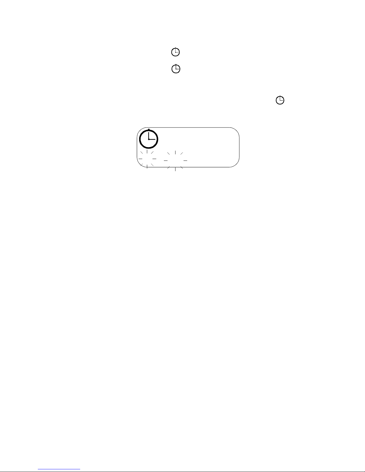
b) The screen shows the time and date with the hour numbers flashing. If the
clock is set to the 12 hour mode, the ‘am/pm’ characters also flash.
c) Use the ¬ or - buttons to set the required hour.
d) Push the O> button again and the tens of minutes number flashes. Set the
required figure with the ¬ or - buttons.
e) Push the O> button to make the minutes number flash. Set the required figure
with the ¬ or - buttons.
f) Push the O> button again and the first number(s) of the date flash. Use the
¬ or - buttons to set the required figures.
g) Push the O> button again and the centre number(s) flash. Set the required
figure with the ¬ or - buttons.
h) Push the O> button again to make the ‘year’ numbers flash. Set the required
figure with the ¬ or - buttons.
i) Push the O> button to select the 12 or 24 hour mode. Use the ¬ or - buttons
to set the required mode.
j) When the display shows the required time and date, push the O> button for
one second to return to the standby screen, or wait for the unit to time-out.
Page 23
Z
11:15pm
6:45am
Z
Z
Z
RPR 583
TM1212 Issue 1 Page 2 - 11
2.2.9 Setting the Timed-off Time
This option sets the pager OFF and ON at preset times (e.g. overnight). To select
this option :
a) Select the Set Time screen as shown in paragraph 2.2.7.
b) Use the ¬ or - buttons to choose the symbol then push the O> button.
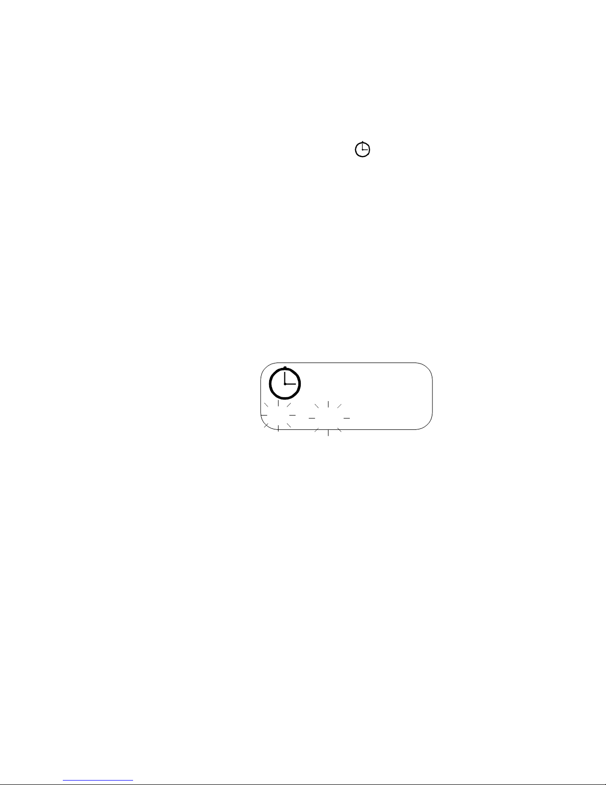
The display shows the Timed-off edit screen.
c) To set the Timed-off option to OFF, push the ¬ or - buttons until the start
and stop times do not show.
d) To set the Timed-off option to ON, push the ¬ or - buttons until the start and
stop times show on the display.
e) To change the START and STOP times:
i) Set the Timed-off option to ON, then push the O> button. The first
numbers (Start Time hours) flash. If the clock is set to the 12 hour mode,
the ‘am/pm’ characters also flash.
ii) Push the ¬ or - buttons to select the required hour.
iii) Push the O> button to select the next number (tens of minutes) then push
the ¬ or - buttons to select the required number.
iv) Push the O> button again to select the next number (minutes) then push
the ¬ or - buttons to select the required number.
v) Push the O> button again to select the next number (Stop Time hours).
vi) Repeat operation ii) through iv) to set the required Stop Time hours and
minutes.
vii) To return to the standby screen, push and hold the O> button for one
second or wait for the unit to time-out.
Page 24

RPR 583
TM1212 Issue1Page 2 - 12
2.2.10 Deleting Messages
a) Deleting Stored or Archived Messages
To delete any message in the store or archive memories of the pager:
i) Select the message with the ¬ or - buttons. Use the O> button to read
the complete message.
ii) When the last screen is displayed, push the O> button then use the
¬ or - buttons to select the delete symbol.
iii) Push the O> button. The display shows the delete symbol plus a
flashing ?
iv) Push the O> button to delete the message.
b) Deleting All Stored Messages
All the messages in the store memory (but not those in the archive memory) can
be deleted in one operation:
i) From the Standby Screen, push the O> button to show the main menu
symbols.
ii) Use the ¬ or - buttons to choose the symbol.
iii) Push the O> button to select the function.
iv) The display shows the symbol plus a flashing ? symbol.
v) Push the O> button to delete all the messages.
c) Auto Delete (Optional Feature)
The unit has a programmable option which allows messages that have been
read to be deleted automatically. The option does not delete ‘unread’ or
‘archived’ messages.
The messages are deleted once a day, at midnight, and the unit can be
programmed to delete the messages after either two days or seven days.
Page 25

RPR 583
TM1212 Issue 1 Page 2 - 13
2.2.11 Switching the Unit OFF
The pager can be switched OFF but the pager cannot receive messages while it is
set to this state. To switch the pager OFF:
a) Select the OFF function on the main menu as shown in paragraph 2.2.2
b) The display shows the symbol plus a flashing ? symbol.
c) Push the O> button to set the pager to OFF.
d) The screen goes blank.
Page 26

RPR 583
TM1212 Issue1Page 2 - 14
2.3 RECEIVING AND STORING MESSAGES
2.3.1 Introduction
The unit is programmed with four RIC addresses which are set to receive different
types of message and which have different audible alerts.
RIC1 Receives personal messages.
The audible alert uses Multitone Beep Codes. Optionally, RIC1 may be
programmed to receive ‘personal alerts’. With this option, the alert is
chosen by the operator from seven allocated sounds (see paragraph
2.2.5).
RIC2 May be programmed to receive personal messages or to receive group
and ‘all call’ messages.
The audible alert uses Multitone Beep Codes plus warble.
RIC3 May be programmed to receive personal messages or to receive group or
‘all call’ messages.
The audible alert uses Multitone Beep Codes only.
RIC4 Receives information services. A maximum of eight information services
can be accommodated, with each service storing a maximum of ten
messages. Optionally, each service can be programmed to determine the
number of messages it can store.
The audible alert can be programmed ON or OFF for each information
service.
The unit can receive tone or alphanumeric messages sent on one of the Multitone
Beep Codes. Group calls can be allocated for a maximum of 10, 100 or 1000 users.
2.3.2 Receiving a Message
When the pager receives a new message the first part of the message shows on the
display and the alert operates. If the standby screen is not showing when the
message is received, or if another message is on the screen, the new message will
be put in the Message Store.
Push any button to acknowledge receipt of the message and to stop the alert.
Page 27

RPR 583
TM1212 Issue 1 Page 2 - 15
If the call is not acknowledged, the pager may be pre-programmed to give a short
alert every two minutes until the battery is exhausted.
If the message is longer than the screen can show, push the O> button to show the
next part of the message. Repeat the procedure until the end of message symbol œ
shows.
To process the message, push the O> button again to show the Reviewing Stored
Messages menu (refer to paragraph 2.3.3).
To return to the standby screen, push and hold the O> button for one second or wait
for the unit to time-out. If the message has not been read, the standby screen will
show the symbol.
2.3.3 Reviewing Stored Messages
To display the received messages, starting with the newest message, push the
- button. The message is displayed with its time and date stamp. If the message
is longer than the screen can show, push the O> button to show the next part of the
message. To read another message, use the ¬ or - buttons.
When the last part of the message is shown, push the O> button. The display shows
three symbols:
To read the message again, use the ¬ or - buttons to select the first symbol then
push the O> button.
To delete the message, use the ¬ or - buttons to select the second symbol then
push the O> button. The display shows the delete symbol plus a flashing ? symbol.
Push the O> button again to delete the message.
To put the message in the Archive Store, use the ¬ or - buttons to select the third
symbol then push the O> button. The display shows the archive symbol plus a
flashing ?. Push the O> button again to transfer the message to the Archive Store.
To return to the standby screen at any time, push and hold the O> button for one
second or wait for the unit to time-out.
The unit memory can hold a maximum of 64 messages. When this number is
reached the standby screen shows the memory full symbol.
If a new message is received when the memory is full, the oldest message is deleted.
Messages which have been read will be deleted before unread messages.
Page 28

RPR 583
TM1212 Issue1Page 2 - 16
2.3.4 Archiving Messages
Messages can be protected by transferring them to the Archive Store. Refer to
paragraph 2.2.3 or paragraph 2.3.2. for the procedure.
2.3.5 Reviewing Information Service Messages (Optional Feature)
When this feature is available, the standby screen shows the symbol when the
pager receives an Information Service message. An audible alert may sound if the
information service has been so programmed.
To select the Information Service menu, make sure the screen shows the standby
display, then push the ¬ button.
The menu screen shows a maximum of eight number symbols, each enclosed within
a circle. Numbers which have unread Information Service messages have a thicker
circle.
Use the ¬ or - buttons to choose the required service number then push the
O> button to show the message.
To review other messages on the same service, push the ¬ or - buttons until the
required message shows.
To return to the Information Services menu push the O> button until the screen
shows these symbols:
Use the ¬ or - buttons to choose the first symbol then push the O> button.
To put the information service message into the Archive Store, use the ¬ or -
buttons to choose the second symbol, then push the O> button. When the ? shows
on the screen, push the O> button again to transfer the message to the archive.
2.3.6 Out of Range (Optional Feature)
When this feature is available, the standby screen shows the No Service symbol if
the pager cannot receive signals from the paging network.
The unit can also be programmed to give an audible alert when the symbol shows
on the screen.
Page 29
A
B
PUSH THE LONG EDGE OF THE
BATTERY DOOR UPWARDS TO OPEN IT
PUSH THE DOOR LOCK TO
RELEASE THE BATTERY DOOR
SLIDE THE BATTERY DOOR
FORWARD
TAG11343-1
RPR 583
TM1212 Issue 1 Page 2 - 17
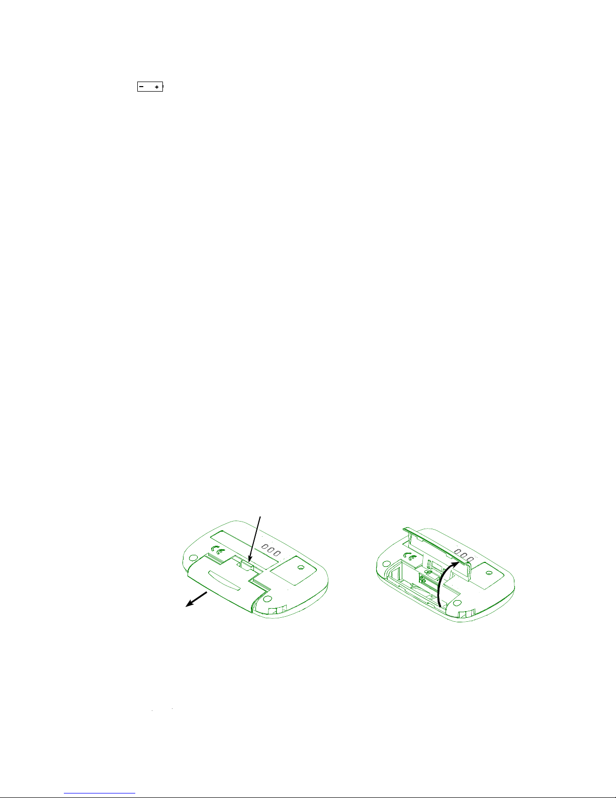
Figure 2.3: Opening the Battery Door
2.4 LOW BATTERY
2.4.1 Low Battery Warning (Optional Feature)
When this feature is available, the standby screen shows the Low Battery symbol
when the unit battery needs replacing.
The unit can also be programmed to give an audible alert when the symbol shows
on the screen.
NOTE: Rechargeable batteries give a lower voltage than disposable batteries.
This can cause the low battery warning system to operate earlier than
necessary. If rechargeable batteries are used, it is recommended that the
Low Battery warning system is not selected.
2.4.2 Replacing the Battery
a) Set the Pager to OFF (see paragraph 2.2.11). Failure to do this will cause all
stored messages to be deleted and the clock to be reset.
b) Refer to Figure 2.3. Use a thumbnail to press down on the battery door lock on
the back of the unit. Hold the door lock down and push the battery door in the
direction shown. Rotate the door as shown in Figure 2.3 to gain access to the
battery.
c) Remove the old battery.
d) Refer to the diagram in the battery compartment and install the new battery.
Page 30

7 9 6
ABSENT
RPR 583
TM1212 Issue1Page 2 - 18
2.4.3 Charging Rack
When the unit is fitted with a rechargeable battery, the battery can be recharged
in situ by placing the complete unit in a Multitone Absence/Charging Rack designed
for the unit. This will be one of the following:
A3RU Master Absence/Charging Rack
A3RV Slave Absence/Charging Rack
In addition to charging the battery, the Absence/Charging racks have the facility to
allow the unit to communicate with the base system. Thus, the system administrator
is advised which units are in the rack.
When the unit is put in an Absence/Charging rack, the unit screen shows a message
on the top line and a user number on the lower line, as shown . Both the message
and the user number can be changed by the system administrator when the unit is
in the rack. The user number appears on the standby screen as the ‘nameplate’
number when the unit is in normal use.
Page 31
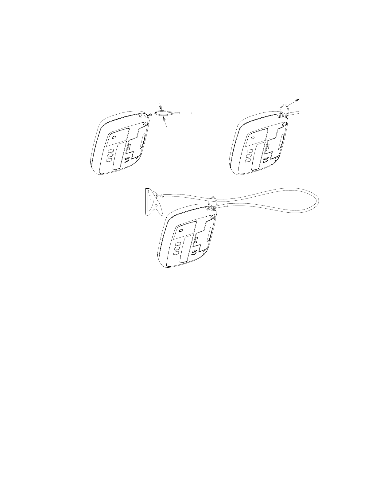
STAGE 1
SQUEEZE THE LOOP TOGETHER
AND PUSH IT INTO THE SLOT
STAGE 2
PULL THE LOOP THROUGH THE
SLOT AS FAR AS POSSIBLE
STAGE 3
FEED THE CLIP THROUGH
THE LOOP AND PULL TIGHT
TAG11372-1
RPR 583
TM1212 Issue 1 Page 2 - 19
Figure 2.4: Lanyard Assembly
2.5 LANYARD ASSEMBLY
Figure 2.4 shows the method of assembling the lanyard to the unit.
Page 32

RPR 583
TM1212 Issue1Page 2 - 20
INTENTIONALLY BLANK
Page 33

RPR 583
TM1212 Issue 1 Page 3 - 1
SECTION 3
TECHNICAL DESCRIPTION
CONTENTS: Page
3.1 CIRCUIT SUMMARY 3 - 2
3.2 DUAL CONVERSION RECEIVER 3 - 4
3.3 DECODER 3 - 7
3.3.1 General 3 - 7
3.3.2 Message Decoder 3 - 7
3.3.3 Microprocessor 3 - 8
3.3.4 EEPROM 3 - 8
3.3.5 SRAM 3 - 8
3.3.6 LCD Module 3 - 8
3.3.7 Display Illumination 3 - 9
3.3.8 Alerts 3 - 9
3.4 POWER SUPPLIES 3 - 9
FIGURES:
3.1 RPR 583 Block Diagram 3 - 2
3.2 Receiver Block Diagram 3 - 4
3.3 Decoder Block Diagram 3 - 7
Page 34
RADIO BOARD DECODER BOARD
AUDIBLE
ALERT
CHARGING
CONVERSION
RECEIVER
DUAL
OSCILLATOR
32.768kHz
VDD
DECODER
CONVERTER
SUPPLY
VOLTAGE
BACK-UP
LIQUID
EEPROM
CRYSTAL
DISPLAY
MODULE
SRAM
M
DISPLAY
LAMP
VIBRATE
MOTOR
MICRO-
PROCESSOR
B+
VDD
PL401 SK1
TAG11340-1
DATA
ADDR
CONTROL
B+
VDD
B+
VDD
GND
CHARGE
PROG
LOWBAT
CHG
RXEN
CHGDET
DATA
BATTERY
DETECTOR
BATTERY
RPR 583
TM1212 Issue 1
Page 3 - 2
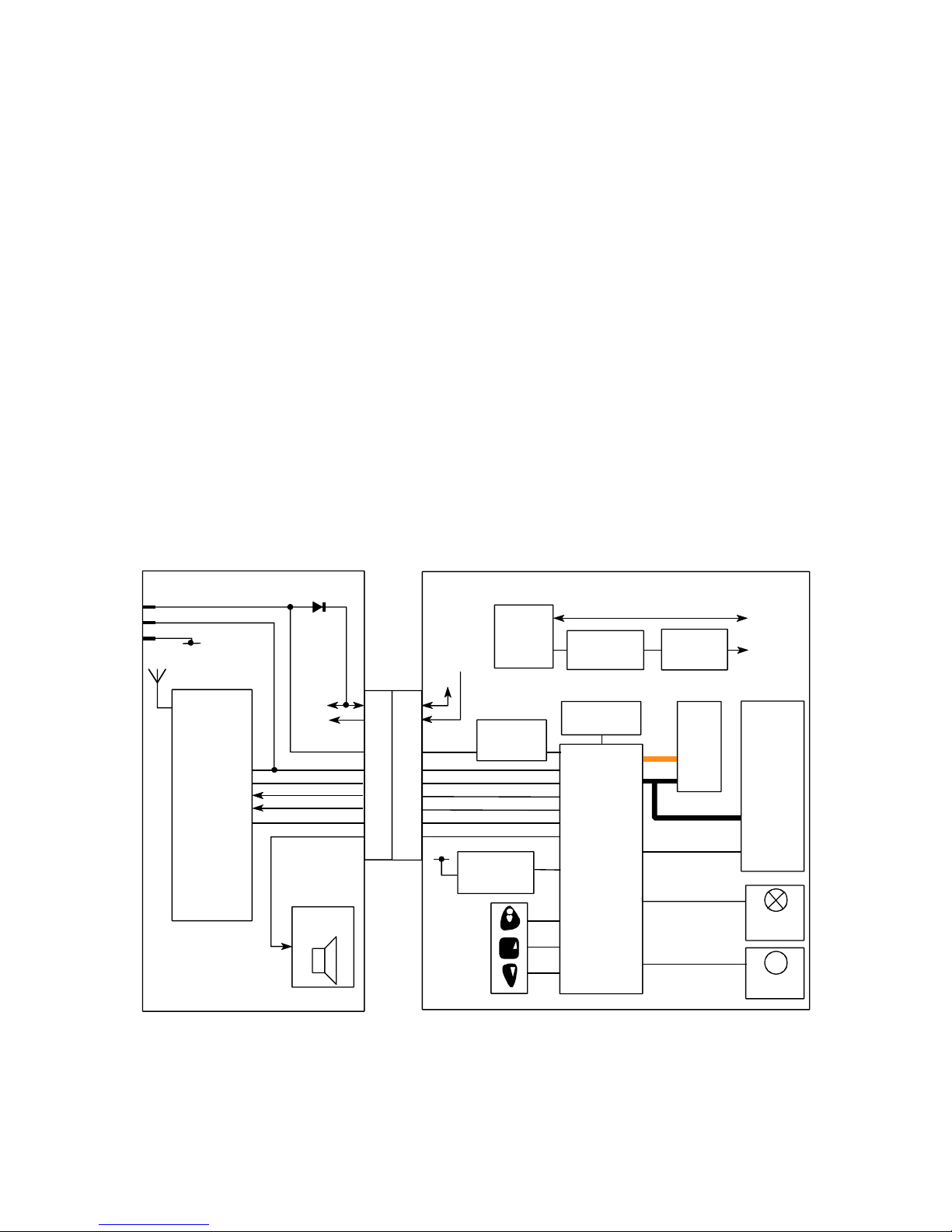
Figure 3.1 RPR 583 Block Diagram
3.1 CIRCUIT SUMMARY
The RPR 583 message receiver consists of two Printed Circuit Board (PCB)
assemblies contained in a plastic case.
The case is constructed in two main parts, the case front and the case back. A
cover on the back of the RPR 583 provides access to the battery compartment. The
two boards in the case are:
a) The Radio Board which has the Dual Conversion Receiver, the 1 volt
regulator and the audio alert output circuit and transducer.
b) The Decoder Board which has the microprocessor, the Decoder Oscillator,
the EPROM, the SRAM, the Liquid Crystal Display Module, the LCD
illumination lamp, the vibrate motor and the primary and backup power
supplies.
The block diagram of the functional areas of the RPR 583 is shown in Figure 3.1.
Refer to Section 7 for the circuit diagram and board layout information.
Page 35

RPR 583
TM1212 Issue 1 Page 3 - 3
The RF signal enters the aerial and is fed to the dual conversion superheterodyne
receiver. The signal is demodulated from RF to baseband frequencies, converted
to digital format and is then fed to the decoder. This results in the received data
activating the memory, display and the selected audible alert or vibrate alert.
To prolong the life of the battery, the receiver operates with battery economy mode.
When the unit is in standby mode, the receiver is powered up at regular intervals
(equivalent to once per batch) to allow the decoder to search for pre-amble. While
the unit is receiving preamble on its allocated channel, the receiver remains powered
up. This allows the decoder to search for a SYNC word. When the SYNC word is
found, ‘batch lock’ is achieved. In batch lock the receiver is only powered up during
the allocated frame to allow the MK7 decoder to search for its address. If the
address is found, the receiver stays ON for the duration of the message.
Page 36
RF AMPLIFIER
TR403
MIXER
AE401
AE402
2nd OSC.
MIXER
455kHz
TR401, TR402
45 MHz
CER
FL402
IC401
MIXER, IF AMP & DET.
TR410, TR414
1st OSC.
FL401
IF AMP
XL402
XL401
TAG11120-1
455kHz
CER
FL403
CV404
AGC CONTROL
TR407
TP403
IMAGE
FILTER
GND GND
CV407
CV406
CV405
TP405
RSSI
DET
DELAY
FL404
DECODER
TP401
SINAD
FSK
COMP.
FILTER
QUICK
CHARGE
AMP
PHASE
1V
REG
TR406
1V
SUPPLY
1V
TP402
INT.
REF.
RXEN
LOWB
RPR 583
TM1212 Issue 1
Page 3 - 4
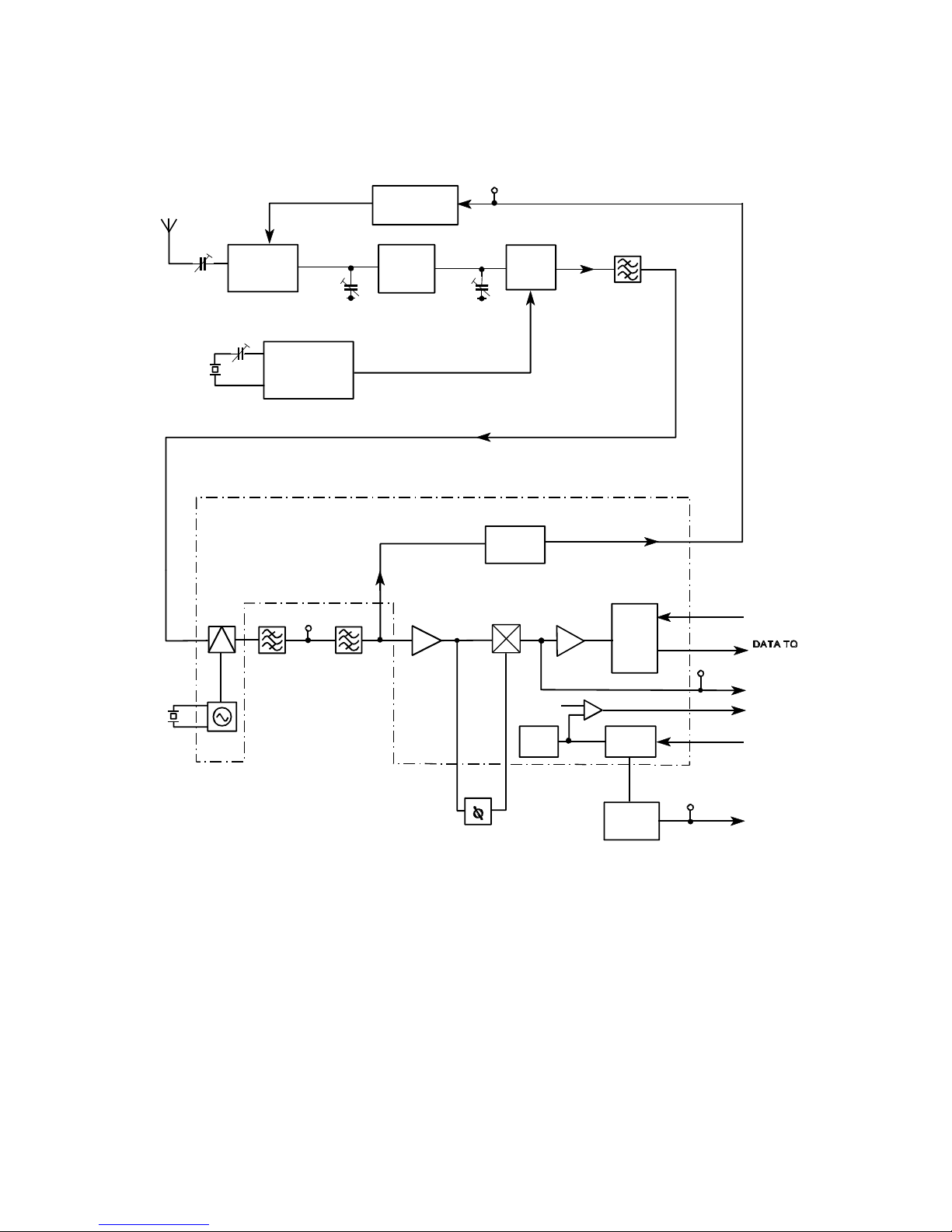
Figure 3.2 Receiver Block Diagram
3.2 DUAL CONVERSION RECEIVER
The incoming RF signal is received by the aerial AE401/AE402 which is tuned by
CV404. Capacitors C401 and C441 provide matching to RF amplifier TR401,
TR402. R401, R402 and TR407 provide AGC.
Page 37

RPR 583
TM1212 Issue 1 Page 3 - 5
Output from the RF amplifier passes through an image filter which provides these
functions:
a) Attenuation of the first image frequency.
b) Attenuation of signals outside the required band.
c) Matches the output impedance of the RF amplifier to the input impedance of
the mixer stage.
C406, L401 and CV407 form a parallel tuned circuit with the resonant frequency
adjusted for minimum loss at the frequency of operation.
C428, CV406 and L407 also form a parallel tuned circuit adjusted for minimum loss
at the frequency of operation. In addition, C428 and L407 form a series resonant
circuit with the resonant frequency close to the first image frequency. The complete
filter network gives approximately 40dB of attenuation at the image frequency.
The local oscillator comprises transistor TR410, crystal XL402 and associated
components. Frequency adjustment is by CV405. The local oscillator frequency is
calculated as follows:
carrier frequency - 45MHz
fx =
3
where fx is the crystal frequency in MHz.
The collector of TR410 is tuned to the third harmonic of XL402 by L411 and C459.
The circuit provides the correct Local Oscillator frequency and reduces the level of
2nd, 4th and higher harmonics. The two tuned circuits, L413, C463 and L415, C464
give further filtering of unwanted harmonics.
The mixer circuit, TR403 and associated components, receives the output of the
image filter. This is mixed with the local oscillator output to produce a 45MHz
product which is selected by the resonant circuit L406, C451. The 45MHz output
passes through a monolithic crystal filter, FL401, which has a bandwidth of ±7.5kHz
at the -3dB points.
The output from FL401 is fed to IC401 pin 24. IC401 is a combined mixer/ local
oscillator/IF/detector.
The second oscillator runs at 44.545MHz (45.455MHz for Band 4) and, with the
exception of XL401 and its associated components, is built into the IC. As the
second oscillator is not trimmed, small frequency errors are absorbed when tuning
the first local oscillator.
The input at pin 24 is applied to the internal second mixer, and is mixed with the
second oscillator output to produce a 455 kHz 2nd IF signal at pin 3. The IF signal
then passes through two ceramic filters FL402 and FL403 which remove unwanted
mixer products and provide further selectivity.
Page 38

RPR 583
TM1212 Issue 1
Page 3 - 6
The output from FL403 is split: one output connects through C450 to pin 6 of IC401
and the IF amplifier; the other connects to the Received Signal Strength Indicator
(RSSI) circuit in IC401 through C419, R407 and pin 5.
Due to the characteristics of filters FL401, FL402 and FL403, the signal at the input
to the IF amplifier has amplitude modulation (AM). The AM must be removed before
the signal reaches the detector stage. This is performed by the IF amplifier in IC401
which has very high gain and is designed to limit the amplitude of the signal to
remove the AM component and give a ‘square’ output. C479 and C480 provide
de-coupling for the amplifier.
The output from the IF amplifier passes to the detector in IC401. This circuit is a
Quadrature Demodulator which has two inputs. One input connects directly to the
IF amplifier, the other receives the signal from the IF amplifier through a phase delay
circuit connected to pins 9 and 10 of the IC. The phase delay depends on the
frequency of the IF signal and is 90 degrees at the centre frequency of the unit’s
allocated channel. The phase shift is provided by ceramic discriminator FL404,
capacitor C426 and resistor R416.
The RSSI circuit in IC401 provides an Automatic Gain Control (AGC) signal for the
receiver. The circuit detects the received signal strength and gives a DC current
out. R407 sets the level at which the circuit starts to operate. The value of 68
kilohms sets it to approximately 16dB above the sensitivity threshold. The DC output
from pin 22 of the IC connects to the AGC control circuit. When there is no RSSI
output, transistor TR407 is biased on and keeps the RF amplifier at full gain. At
strong signal levels the output from the RSSI causes TR407 to cut off gradually, thus
reducing the gain of the RF amplifier. C437 determines the rise and fall times of the
AGC.
The output from the detector stage, pin 11, gives an audio output to TP401. This
test point is used in the final stages of production to align the receiver circuits.
TP401 is also used to program the decoder section of the unit and connects to the
microprocessor (IC3) on the decoder board through PL401/SK1, pin 13. In addition,
pin 13 connects to the external PROG connection on the back of the unit, which
allows the microprocessor to communicate with the paging management system,
when the unit is in the ‘Absence/Charging Rack’.
Pin 11 of IC401 also connects to pin 12 through R425, R429 and R428. These
resistors together with capacitors C448, C483, C484 and the internal filter amplifier
of IC401 form the data filter; a unity-gain, low-pass filter which reduces high
frequency noise. The output of the filter amplifier connects internally to the FSK
Comparator. The data output of the comparator, pin 18, connects to microprocessor
IC3, pin 36 through PL401/SK1, pin 11. A logic signal from IC3, pin 58 to IC401, pin
16 controls the Fast/Slow charge of the comparator. The logic level at pin 16 is
always set high.
Page 39
LIQUID
EEPROM
CRYSTAL
DISPLAY
MODULE
SRAM
M
AUDIBLE
ALERT
VIBRATE
MOTOR
MICRO-
PROCESSOR
SK1PL401
TAG11341-1
DATA BUS
ADDRESS BUS
CONTROL LINES
OSCILLATOR
PGM
DATA
XL2
SW2
SW3
SW1
!>BUTTON
BUTTON
BUTTON
FROM / TO
RECEIVER
RESET
IC5
VDD
IC1
IC3
TR7
RESET
DRIVER
DRIVER
TR415
TR3; TR4
TP401
DRIVER
TR2
TR416
DISPLAY
LAMP
SK1 PL401
IC4
RESET
PROG
FSTCHG
RXEN
LOWB
PROG
CHARGE
DETECT
CHARGING
DETECTOR
BATTERY
TR5
TR6
32.768
KHz
RPR 583
TM1212 Issue 1 Page 3 - 7
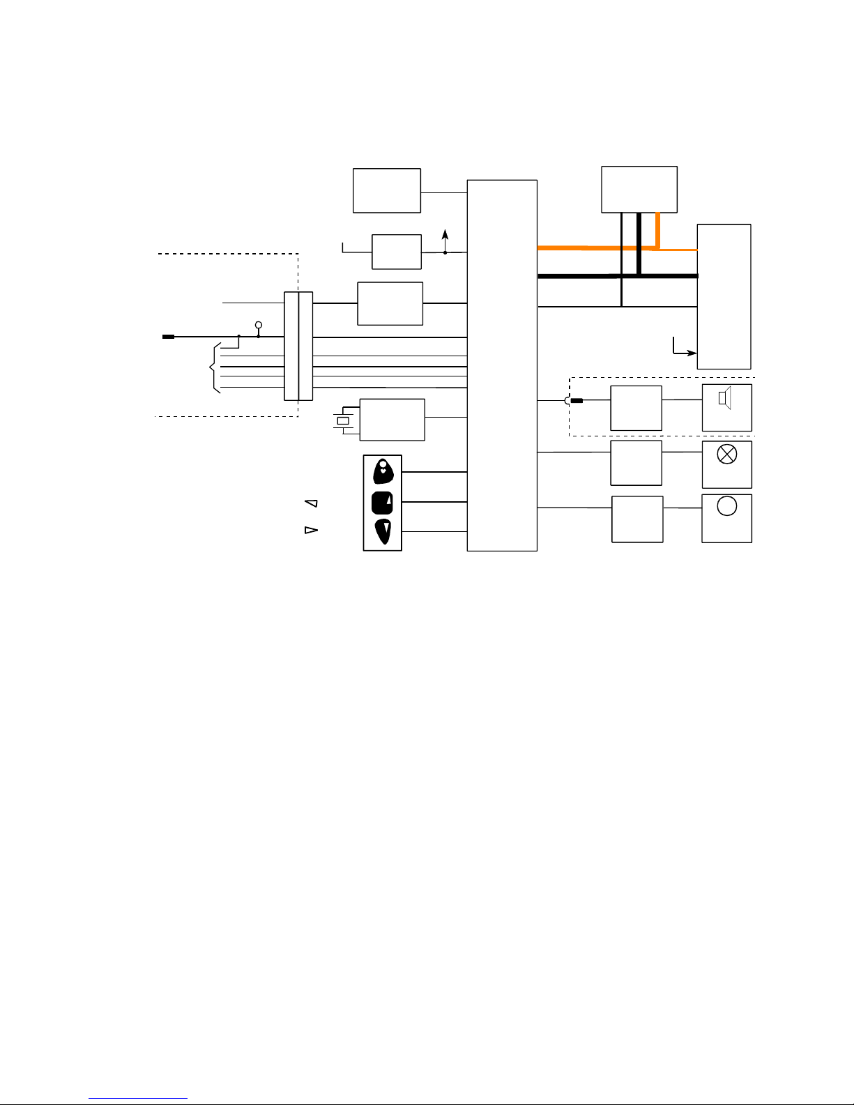
Figure 3.3 Decoder Block Diagram
3.3 DECODER
3.3.1 General
The Decoder comprises the Decoder Oscillator, Microprocessor, EEPROM, SRAM
message memory and switches, plus support components and a separate LCD
module. The signal from the receiver is processed by the decoder software in the
microprocessor. The microprocessor stores the information in the SRAM, IC4,
before activating the selected alert and sending the message data to the LCD
module for display. The EEPROM holds information applicable to the unit.
3.3.2 Message Decoder
The Microprocessor, IC3, contains software to process data signals received in
Multitone Mk7 format. When no valid signals are received by the unit, the system
goes into a standby mode to reduce power consumption.
Page 40

RPR 583
TM1212 Issue 1
Page 3 - 8
3.3.3 Microprocessor
The microprocessor controls the functions of the unit. A 4.19MHz clock controlled
by XL1, provides the basic timing for the system.
A second clock (TR5, TR7, XL2) provides pulses at 32.768kHz, to operate the
microprocessor while it is in standby mode.
Data received from IC401 is processed by the microprocessor and stored in the
SRAM chip, IC4. The microprocessor then causes the selected Alert to operate and
sends the message to the LCD module for display. Outputs from pin 5 (LCD-CS),
pin 39 (AD17), pin 38 (AD16) and pin 60 (/WR) control the transfer of data to the
LCD module. Outputs from pins 2, 7 and 8 control the operation of the audio alert,
the vibrate motor and the display backlight lamps.
IC3 also controls the internal functions of the system, displaying the symbols and
changing the modes when selected by the three buttons on the front of the unit.
Putting the unit in the rack also connects the microprocessor’s PGM input (pin1) to
the paging system controller through the PROG contact at the rear of the unit. This
allows communication between the unit and the system controller.
3.3.4 EEPROM
The EEPROM (IC1) holds information applicable to the unit, such as: Serial Number;
RIC codes; Radio parameters; Programmed options. The information is sent to the
microprocessor through the serial data link, pins 62, 63 and 64.
3.3.5 SRAM
The SRAM (IC4) is a 256 k device which can store up to 32 k of 8-bit information.
Address lines AD00 through AD14 and control lines RAM-CE and /WR from the
microprocessor, control the flow of data in and out of the device.
3.3.6 LCD Module
The LCD Module is a single device which contains all the necessary circuits to
produce the alpha-numeric characters and the symbols for the integral display.
Address lines AD16 and AD17 and control lines LCD-CS and /WR from the
microprocessor, control the flow of data to the device.
C20 and C21 (pins 27 through 30) are part of the internal DC/DC converter of the
module’s negative bias supply.
R11, R12, R13, C17 and C22 through C25 are part of the circuit which controls the
voltage to the LCD driver.
Page 41

RPR 583
TM1212 Issue 1 Page 3 - 9
3.3.7 Display Illumination
One miniature lamp is used to illuminate the LCD display. The lamp is selected ON
or OFF using the buttons on the front panel. The ‘Lamp ON/OFF’ signal, which
comes from pin 8 of the microprocessor, controls transistor TR2 in the lamp circuit.
3.3.8 Alerts
a) Audible Alert (Beep)
The transducer, SP401, and the driver circuits TR415 and TR416, are installed
on the radio board. The audible alert signal from IC3, pin 2 connects to TR415
through SK1/PL401 pin14. The alert can be selected ON or OFF using the
buttons on the front panel.
b) Vibrate Alert
The vibrate motor is operated by transistors TR3 and TR4 on the decoder
board. The vibrate alert signal from IC3, pin 7 connects to pin 1 of TR3. The
alert can be selected ON or OFF using the buttons on the front panel.
3.4 POWER SUPPLIES
The primary power supply for the unit is a single 1.5 volt, AAA battery (BAT1). The
supply from the battery (B+) connects directly to the lamp and vibrate motor circuits
that require relatively high currents. B+ also connects to the radio board through
SK1/PL401, pin 9 and to the voltage converter, IC6, on the decoder board.
IC6 and its associated components supply the +3.0 volts (VDD) for the unit. In
addition, the circuit charges the backup supply (BAT2) through resistor R6. Double
diode D2 provides isolation for the two circuits.
IC5 is configured to monitor Vdd and resets the decoder circuits if the voltage would
cause data corruption.
Transistor TR1, connected to pins 6 and 15 of IC3, detects the battery voltage. If
BAT1 is removed, the drop in B+ causes transistor TR1 to switch OFF which sets the
microprocessor to low-current mode. In this mode BAT2 supplies sufficient power
to keep the microprocessor and the SRAM operational for more than 5 minutes.
The 1 volt supply for the receiver circuits is provided by transistor TR406 and its
associated components. The circuit is a series regulator and is maintained within
specification by a control circuit in IC401.
Page 42

RPR 583
TM1212 Issue 1
Page 3 - 10
INTENTIONALLY BLANK
Page 43

RPR 583
TM1212 Issue 1 Page 4 - 1
SECTION 4
INSTALLATION AND COMMISSIONING
There are no installation and commissioning procedures for the RPR 583 unit.
Page 44

RPR 583
TM1212 Issue 1Page 4 - 2
INTENTIONALLY BLANK
Page 45

RPR 583
TM1212 Issue 1 Page 5 - 1
SECTION 5
SERVICING
CONTENTS: Page
5.1 SERVICE POLICY 5 - 3
5.2 ROUTINE MAINTENANCE 5 - 3
5.3 WORKSHOP PROVISIONS 5 - 3
5.4 TEST EQUIPMENT, TOOLS AND ANCILLARIES 5 - 3
5.4.1 Test Equipment 5 - 3
5.4.2 Tools and Ancillaries 5 - 4
5.5 DISASSEMBLY 5 - 4
5.5.1 Case Removal 5 - 4
5.5.2 Board Assembly Removal 5 - 5
5.5.3 Board Separation 5 - 5
5.5.4 LCD Module Removal 5 - 6
5.5.5 Vibrate Motor Removal 5 - 6
5.5.6 Battery Contacts Removal 5 - 6
5.6 ASSEMBLY 5 - 6
5.6.1 Battery Terminal Installation 5 - 6
5.6.2 Vibrate Motor Installation 5 - 6
5.6.3 LCD Module Installation 5 - 8
5.6.4 Board Assembly 5 - 8
5.6.5 Board Assembly Installation 5 - 8
5.6.6 Case Assembly 5 - 8
5.7 FAULT FINDING 5 - 9
5.7.1 General 5 - 9
5.7.2 Fault Diagnosis 5 - 9
5.7.3 Power Supply Voltage Adjustment 5 - 9
5.7.4 Battery-Low Circuit Test 5 - 10
5.8 RADIO ALIGNMENT PROCEDURE 5 - 23
5.8.1 Preparation 5 - 23
5.8.2 Alignment Procedure 5 - 23
5.8.3 Pager Sensitivity Measurement (Coarse) 5 - 25
5.8.4 Pager Sensitivity Measurement (Fine) 5 - 25
5.9 PROGRAMMING 5 - 28
5.9.2 Equipment 5 - 28
5.9.3 Procedure 5 - 28
Page 46

RPR 583
TM1212 Issue 1
Page 5 - 2
TABLES: Page
5.1 Radio Board DC Voltage Levels 5 - 14
5.2 Radio Board Test Points 5 - 14
5.3 Decoder Board DC Levels 5 - 15
5.4 Decoder Board Test Sequence 5 - 15
5.5 Display Module Voltages 5 - 16
5.6 IC3 Microprocessor Pin Connections 5 - 20
5.7 IC4 RAM Pin Connections 5 - 21
5.8 LCD Display Pin Connections 5 - 22
FIGURES:
5.1 Battery Door 5 - 4
5.2 Case Front Removal 5 - 5
5.3 Exploded View of Unit 5 - 7
5.4 Connections between Radio Board and Decoder Board 5 - 10
5.5 Fault Finding Guide (Sheet 1 of 3) 5 - 11
5.6 Fault Finding Guide (Sheet 2 of 3) 5 - 12
5.7 Fault Finding Guide (Sheet 3 of 3) 5 - 13
5.8 Display Module Connections 5 - 16
5.9 Decoder Board Waveforms 5 - 17
5.10 Display Module Waveforms 5 - 18
5.11 Semiconductor Connection Details 5 - 19
5.12 Radio Alignment Test Equipment 5 - 23
5.13 P671A Showing the Tuning Points 5 - 24
5.14 Configuration for Coarse Sensitivity Measurement 5 - 25
5.15 Polystyrene Block for TEM Cell Test - Dimensions 5 - 26
5.16 Programming Lead Connections 5 - 27
CAUTION
STATIC SENSITIVE DEVICES ARE USED IN THIS EQUIPMENT. TAKE CARE DAMAGE
IS NOT CAUSED TO THESE DEVICES BY HIGH LEVELS OF STATIC ELECTRICITY.
Page 47

RPR 583
TM1212 Issue 1 Page 5 - 3
5.1 SERVICE POLICY
Except for Routine Maintenance, repairs are only to be performed by qualified
personnel in authorised workshops.
The unit can be repaired to component level. The display module is a disposable
item. If any screening cans are removed for access to components, they must be
refitted flush to the printed circuit board.
5.2 ROUTINE MAINTENANCE
This is limited to battery replacement and surface cleaning of the outer case using
a lint free cloth moistened with soapy water. Do not use spirit or other solvents as
they can damage the case.
5.3 WORKSHOP PROVISIONS
Repair workshops must be free from hostile radio interference or otherwise equipped
with Faraday cages. Suitable equipment must be available to remove and install the
surface mounted components which are used in this unit.
5.4 TEST EQUIPMENT, TOOLS AND ANCILLARIES
5.4.1 Test Equipment
The following test equipment is required:
! IBM PC or compatible personal computer
! Programming Software P672A
! P654 Test Encoder + Multitone MK7 Test Encoder Software
! RF Signal Generator (DC FM coupled)
! Oscilloscope
! Millivoltmeter with high impedance, low capacitance probe
! Alignment and Fault -Finding Jig P671, P671A , P671B
! SINAD Meter
! AC Millivoltmeter
! Digital Multimeter
Page 48
A
B
PUSH THE LONG EDGE OF THE
BATTERY DOOR UPWARDS TO OPEN IT
PUSH THE DOOR LOCK TO
RELEASE THE BATTERY DOOR
SLIDE THE BATTERY DOOR
FORWARD
TAG11343-1
RPR 583
TM1212 Issue 1
Page 5 - 4
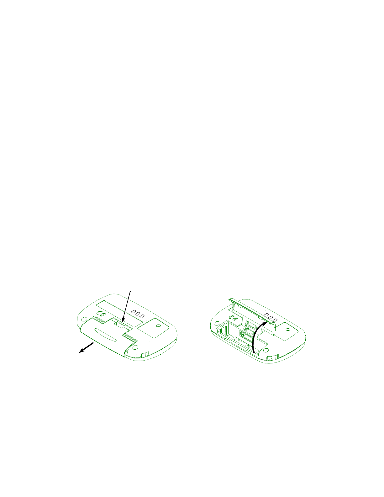
Fig. 5.1: Battery Door
5.4.2 Tools and Ancillaries
The following tools and ancillaries are required:
! DC Power Supply, 1-1.5 volts.
! Cross-point Screwdriver
! Surface Mount Handling Tools
! Anti-static Workstation
5.5 DISASSEMBLY
5.5.1 Case Removal
a) Refer to Figure 5.1. Use a thumbnail to press down on the battery door lock on
the back of the unit. Hold the door lock down and push the battery door in the
direction shown. Rotate the door as shown in Figure 5.1 to get access to the
battery.
b) Remove the battery.
c) Remove the two, 2.2mm x 6mm cross-head screws from the Case Back.
Page 49
APPLY PRESSURE
WITH FINGERS
TO SIDES OF CASE
LIFT FRONT EDGE OF CASE FRONT
UNTIL REAR CATCHES DISENGAGE
TAG11213-1
>
RPR 583
TM1212 Issue 1 Page 5 - 5
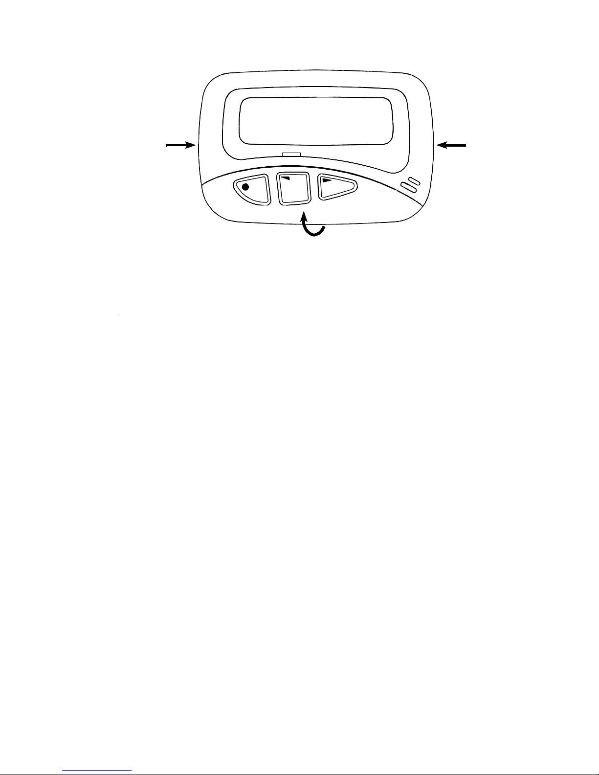
Fig. 5.2: Case Front Removal
d) Remove the Case Back by applying pressure to the sides of the case, as shown
in Figure 5.2, and lifting the front edge of the Case Front until the rear catches
disengage.
5.5.2 Board Assembly Removal
a) Remove the Case Back (see paragraph 5.5.1).
b) Carefully lift the Board Assembly at the long edge next to the LCD Module.
When the edge of the Board Assembly is clear of the case, pull the assembly
away from the case.
5.5.3 Board Separation
a) Remove the Board Assembly from the case (see paragraphs 5.5.1 and 5.5.2).
b) Carefully pull the front edge of the boards apart to disconnect the connector
between the boards.
c) Pull the Decoder Board forward to release the LCD Module from under the
aerial.
d) To get access to the Radio Board components, remove the spacer moulding.
Page 50

RPR 583
TM1212 Issue 1
Page 5 - 6
5.5.4 LCD Module Removal
a) Remove the Board Assembly from the case (see paragraphs 5.5.1 and 5.5.2)
and separate the decoder board from the radio board (see paragraph 5.5.3, a)
through c)).
b) Release the display bezel from the two holes in the Decoder Board and
carefully fold the module away from the board, to get access to the flexible
cable.
c) Use the correct soldering tools to disconnect the flexible cable from the board.
5.5.5 Vibrate Motor Removal
a) Do the procedures given in paragraphs 5.5.1, 5.5.2 and 5.5.3, a) through c).
b) Use the correct soldering tools to disconnect the two wires from the board.
c) Use a screwdriver to lever the Vibrate Motor carefully from the clip.
5.5.6 Battery Contacts Removal
a) Remove the Board Assembly from the case (see paragraphs 5.5.1 and 5.5.2)
b) Pull the contacts out of their slots in the Case Back.
5.6 ASSEMBLY
5.6.1 Battery Terminal Installation
a) Refer to Figure 5.3 for the correct orientation of the terminal.
b) Push the terminal into the slot in the Case Back.
5.6.2 Vibrate Motor Installation
a) Install the Vibrate Motor in the clip.
b) Use the correct soldering tools to connect the two wires to the Decoder Board.
Page 51
3
1
TAG11344-1
2
4
5
6
7
11
13
10
9
8
12
RPR 583
TM1212 Issue 1 Page 5 - 7
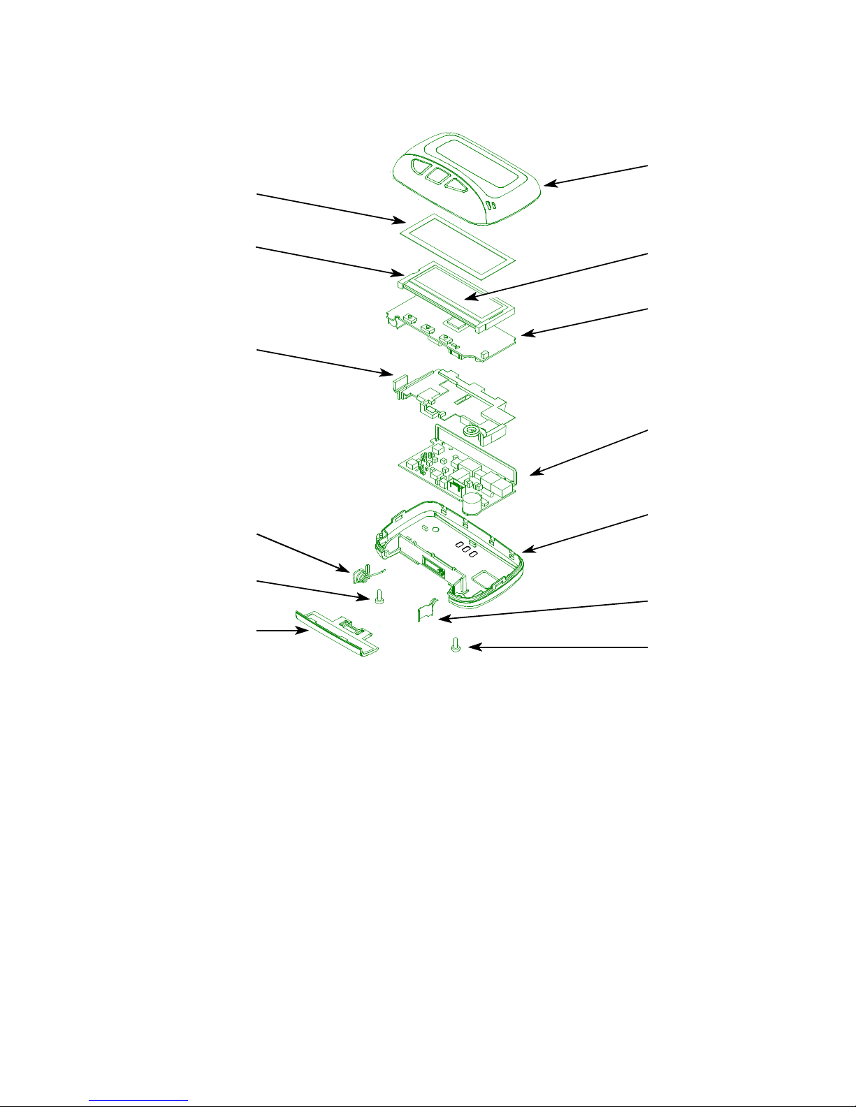
1. Case Front Assembly 8. Battery Door
2. LCD Display 9. Case Fixing Screw
3. Decoder Board Assembly 10. Battery Negative Contact
4. Radio Board Assembly 11. Rubber Mat
5. Case Back Assembly 12. Moulding Bezel LCD
6. Battery Positive Contact 13. Display Gasket
7. Case Fixing Screw
Fig. 5.3: Exploded View of Unit
Page 52

RPR 583
TM1212 Issue 1
Page 5 - 8
5.6.3 LCD Module Installation
a) Clean and tin the pads on the Decoder Board.
b) Use the correct soldering tools to connect the flexible cable to the Decoder
Board.
b) Carefully fold the flexible cable. Position the display bezel over the cable so
that the two pins on the rear of the bezel fit in the holes on the Decoder Board.
5.6.4 Board Assembly
a) Make sure that the Spacer Moulding is correctly installed on the Radio Board.
b) Put the Decoder Board on the Spacer Moulding. Make sure that the four small
extensions at the rear of the LCD Module are located under the aerial.
c) Align SKT1 with PL401 and carefully press the two boards together until the
connectors are fully connected.
5.6.5 Board Assembly Installation
a) Slide the Board Assembly into the Case Back.
b) Make sure that the Battery Connector ‘fingers’ are in the correct position under
the Decoder Board.
c) Push down on the front edge of the board and slide the board under the small
extensions on the Case Back.
d) Push the rear edge of the Board Assembly into the Case Back.
5.6.6 Case Assembly
a) Install the Case Front on the Case Back by applying pressure to the sides of
the case and pushing the rear edges of the case together until the catches snap
in place.
b) Install the two 2.2mm x 6mm screws in the Case Back.
c) Open the Battery Door and install the battery.
d) Close the Battery Door and push it towards the top of the unit until it locks.
Page 53

RPR 583
TM1212 Issue 1 Page 5 - 9
5.7 FAULT FINDING
5.7.1 General
Refer to the Fault Finding Guide (Figures 5.5 through 5.7) and the information given
in Tables 5.1 through 5.9 and Figures 5.8 through 5.11 to help resolve problems.
Alignment information is in paragraph 5.8. Programming information is given in
paragraph 5.9.
Faults can be caused by user negligence. Always check the unit for these faults:
a) Damage to the Case or LCD
b) Water damage
c) Corrosion damage or leaking battery
Any metal parts which are corroded must be removed. Clean the affected area of the
Board assembly with a non-corrosive contact cleaner. Dry the area with a lowpressure flow of warm air (40 EC through 50 EC). Install new parts.
5.7.2 Fault Diagnosis
Put a known good battery in the unit and switch ON the unit. Refer to the Fault-
Finding Guide (Figures 5.5 through 5.7). If it is suspected that the Decoder Board
is faulty, proceed as follows:
a) Remove the Board Assembly from the case (see paragraphs 5.5.1 and 5.5.2).
b) Separate the Decoder Board from the Radio Board (see paragraph 5.5.3).
c) Disable the Battery Economy function by installing a 0 ohm resistor in the
position for R456 (side 2 of the radio board near IC401).
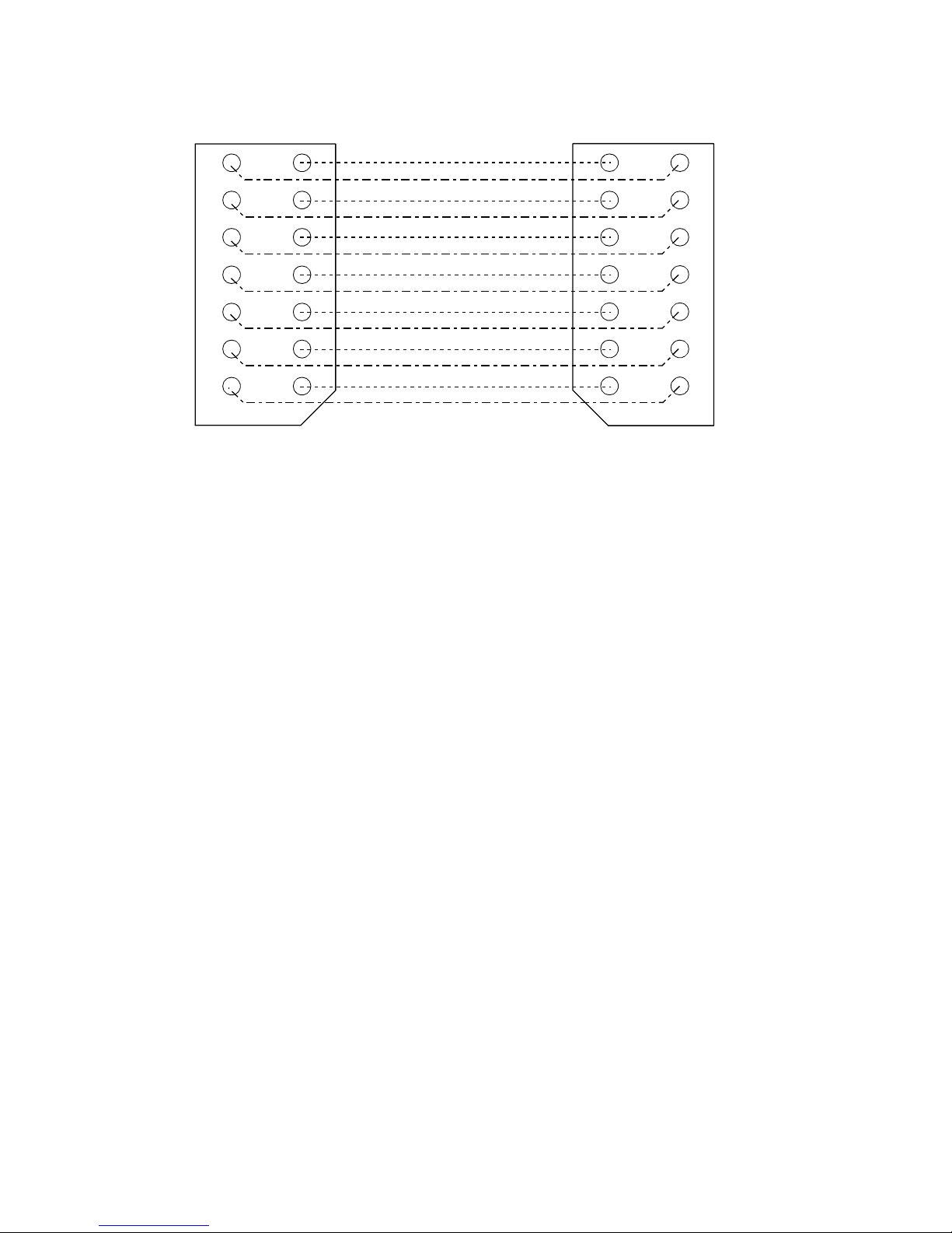
d) Use the 14-way lead (supplied with the P671B) to connect the two boards (refer
to Figure 5.4)
e) Put the boards on an anti-static mat and connect a 1.5 volt supply to the
Decoder Board. Switch ON the power supply.
f) Connect a ’10-times’ probe to the oscilloscope and measure the points given
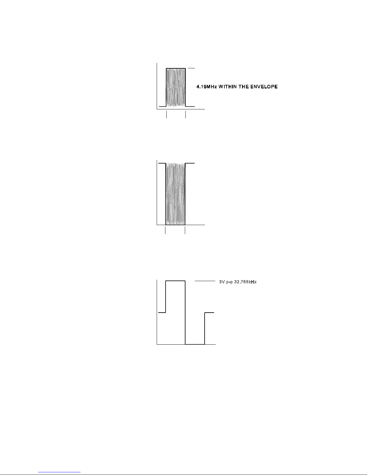
in Table 5.4. Compare the waveforms on the oscilloscope with those shown in
Figure 5.9.
5.7.3 Power Supply Voltage Adjustment
There is no adjustment for the 1 volt, 1.5 volts or 3 volts power supplies.
Page 54
14 1
LOWBAT
N.C.
RXEN
CHGDET
7 7
FSTCHG
BEEP
PGM
N.C.
VDD (+3V)
GND
B+
DATA
1
8
14
8
GND
DECODER BOARDRADIO BOARD
PL401 SK1
N.C.
TAG11345-1
RPR 583
TM1212 Issue 1
Page 5 - 10
Fig. 5.4: Connections between Radio Board and Decoder Board
5.7.4 Battery-Low Circuit Test
To check the Battery-Low circuit:
a) Connect the variable DC power supply to the unit and set the output to
1.05 volts.
b) Switch ON the unit. The unit should go through the normal ‘start-up’ procedure
(beep and vibrate for one second and show the programmable switch-on
message for three seconds). After approximately two minutes the low battery
symbol will appear.
c) Switch OFF the unit. Set the output of the variable DC power supply to
1.2 volts.
d) Switch ON the unit. Make sure that the unit goes through the normal ‘start-up’
procedure.
Page 55
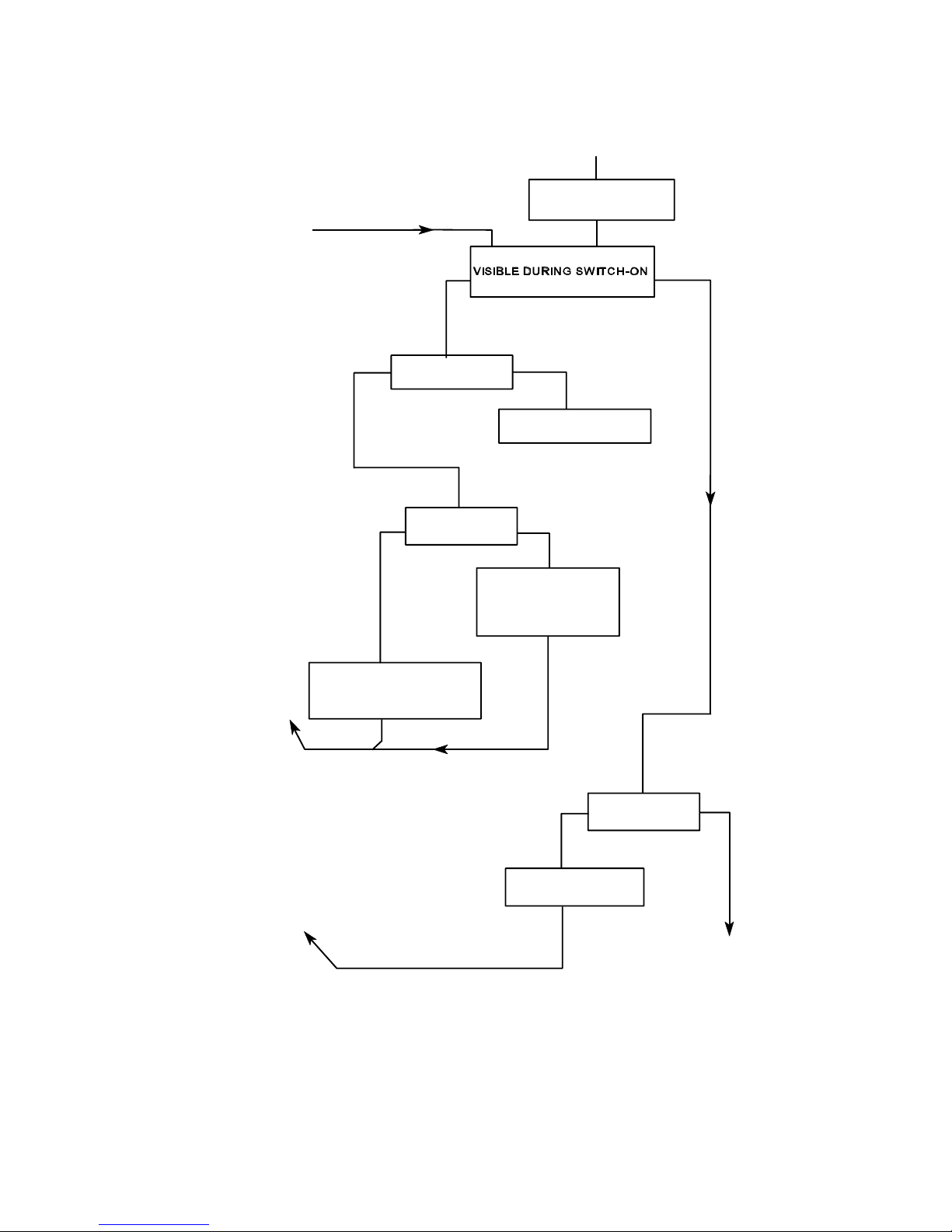
PAGER
SUSPECT
FIT A NEW BATTERY
AND SWITCH ON.
IS THE ‘SWITCH ON’ MESSAGE
IS DISPLAY BLANK
OR CORRUPTED?
CORRUPTED EEPROM.
RE-PROGRAM. RE-TEST.
CORRUPTEDBLANK
NO YES
SEQUENCE?
IS BEEP AUDIBLE
AT SWITCH-ON?
IS BEEP AUDIBLE
AT SWITCH-ON?
DE-CASE AND CHECK
DISPLAY MODULE, VDD
AND
YESNO
DE-CASE AND CHECK
SP401, TR416, TR415.
YES
NO
INTERCONNECTIONS.
DE-CASE AND CHECK
DISPLAY, VDD, IC1, IC3, IC4,
TR5 AND POWER SUPPLIES.
'A'
'A'
'B'
'A'
TAG11346-1
RPR 583
TM1212 Issue 1 Page 5 - 11
Fig. 5.5: Fault Finding Guide (Sheet 1 of 3)
Page 56
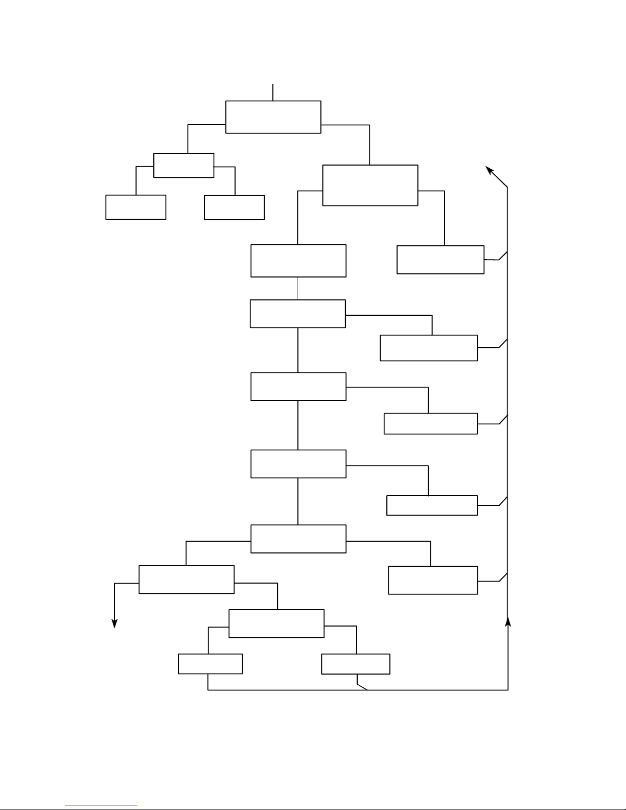
IS CALL RECEIVED?
CHECK
REALIGN AND
DE-CASE.
PLACE IN P671.
CHECK 1V LINE.
IS LEVEL 1V ±50mV?
CHECK TP416, TR406,
IC401.
SEND PRE-AMBLE.
AT 50dBm WITH
±4.5kHz DEVIATION.
IS DATA PRESENT ON
IC401 PIN 18?
IS DATA PRESENT ON
IC401 PIN 12?
CHECK TR408 (IF FITTED)
R412, R463 AND R465
CHECK IC401
IS DATA PRESENT ON
IC401 PIN 11?
IS 455kHz PRESENT ON
IC401 PIN 10?
IS VOLTAGE ON
IC401 PIN 17
>1.3V?
CHECK FL404, C425
IC401 FAULTY.
CHECK R457
CHECK R425, R429
AND IC401.
IS 455kHz PRESENT ON
IC401 PIN 6?
SENSITIVITY.
RECEIVER
RE-TEST
O.K.
NO
LOW
>3dBm
O.K.
YES
NOYES
YES
NO
YES
NO
YES
NO
YESNO
YES
NO
YES
NO
‘B’
‘C’
PLACE THE UNIT IN A
P671. SEND A CALL.
TAG11347-1
‘B’
RPR 583
TM1212 Issue 1
Page 5 - 12
Fig. 5.6: Fault Finding Guide (Sheet 2 of 3)
Page 57
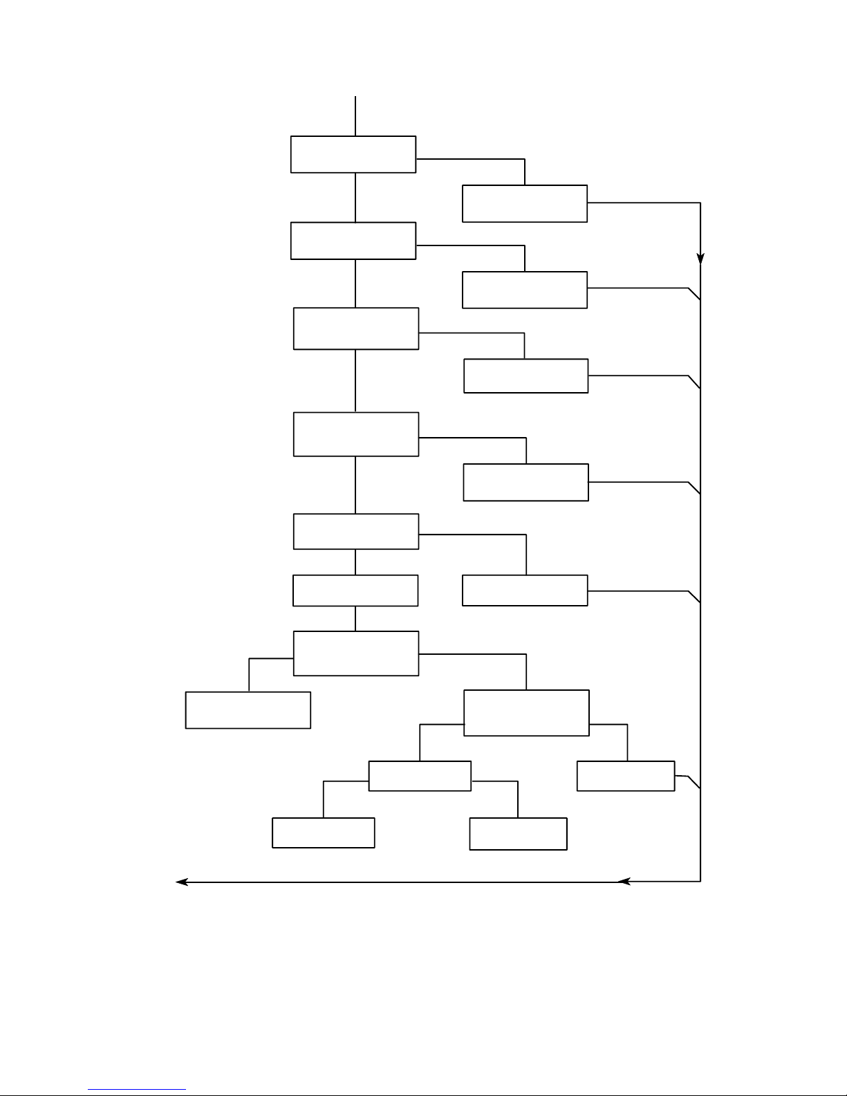
(IC401, PINS 1 AND 2)
>200mV?
REMOVE SHORT FROM
C407/R445 TO 0V.
CHECK XL401
CHECK IC401
IS TR403 (1st MIXER
O/P) >3mV?
CHECK TR414, TR410,
L408 AND XL402.
CONNECT TR410 BASE
CHECK TR403
IS 455kHz PRESENT ON
TP405?
FL403 OR C450 FAULTY.
CHECK FL401, R443
TO 0V. IS RF LEVEL AT
NO
YES
YES
NO
YES
NO
YES
YES
YES
NO
‘C’
SHORT JUNCTION OF
C407/R445 TO 0V.
IS IC401, PIN 24 >3mV?
(TR414 COLLECTOR)
>25mV?
TR403 BASE >3mV?
AND CV407.
IS RF AT TR402
NO
COLLECTOR >3mV?
CHECK TR401,
TR 402 AND L401.
YESNO
YESNO
CHECK C445 AND
TAG11129-1
‘B’
IS 2nd LOCAL OSC. O/P
IS 1st LOCAL OSC. O/P
AND C472.
NO
AND L406.
IS 455kHz PRESENT AT
IC401, PIN 3?
FL402 FAULTY.
YES
NO
NO
RPR 583
TM1212 Issue 1 Page 5 - 13
Fig 5.7: Fault Finding Guide (Sheet 3 of 3)
Page 58
RPR 583
TM1212 Issue 1
Page 5 - 14
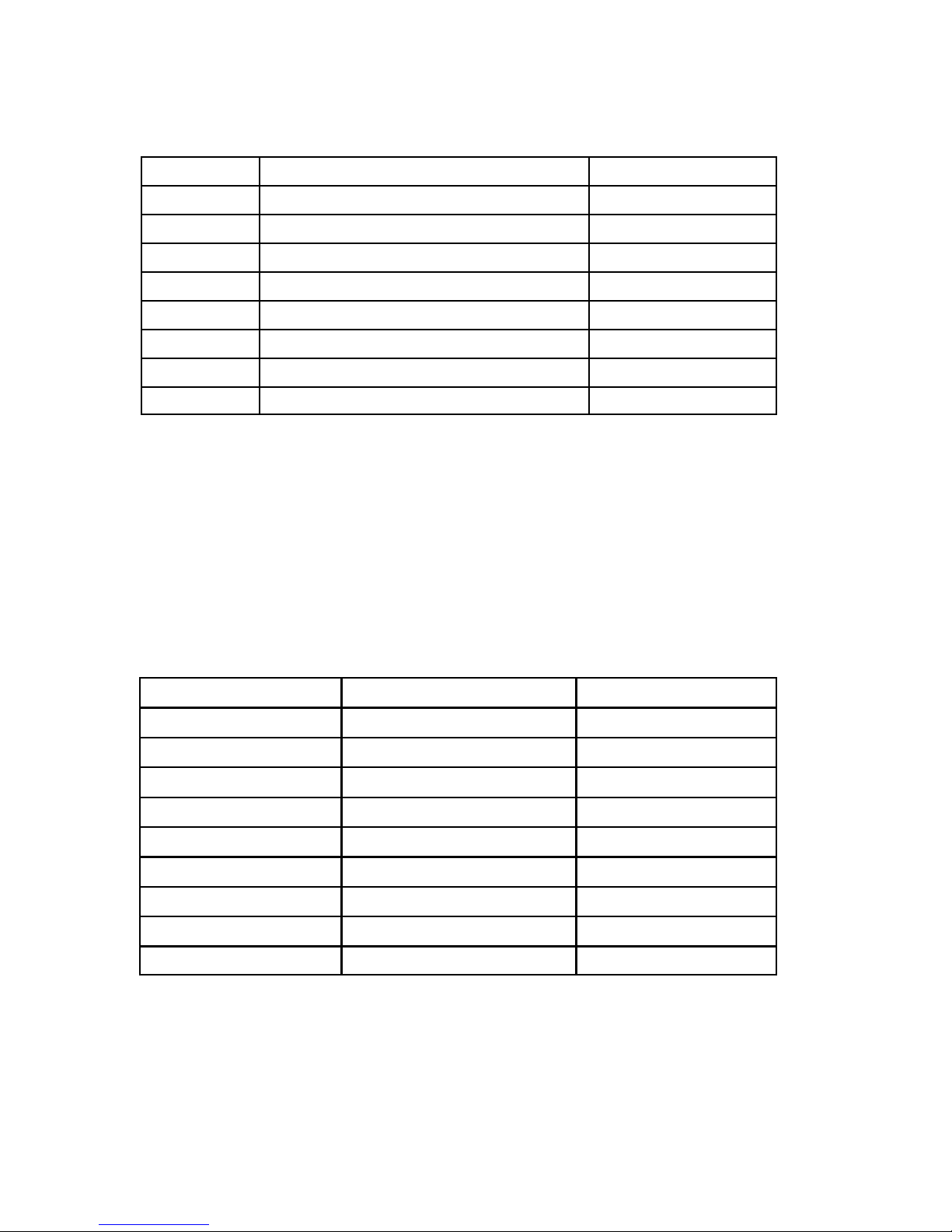
COMPONENT COLLECTOR BASE EMITTER COMMENTS
TR401 0.29 0.73 0 RF Amplifier
TR402 0.87 1.02 0.29 RF Amplifier
TR403 0.845 0.678 0 First Mixer
TR404 0.733 0.015 0 AGC Switch
TR406 1.018 0.791 1.4 1V Series Regulator
TR410 0.95 0.937 0.264 First Local Oscillator
TR415 1.4 - 0 Beep Enable
TR416 1.4 - 0 Transducer Driver
Table 5.1: Radio Board DC Voltage Levels
TEST POINT DESCRIPTION VOLTAGE / SIGNAL
401 Sinad Output 0.56Volts
402 Radio Supply 1 Volt
403 RSSI (AGC) 0.060Volts
404 Radio Ground 0Volts
405 Second IF 455kHz
406 Radio Ground 0Volts
414 Radio Ground 0Volts
416 Battery + 1.4Volts
418 Radio Ground 0Volts
Table 5.2: Radio Board Test Points
NOTE: All radio board measurements were taken with the receiver turned on. The battery terminal
voltage was 1.4 volts, the 1 volt line was 1.019 volts and battery economy was disabled.
Voltages may vary by ±20mV.
Page 59
RPR 583
TM1212 Issue 1 Page 5 - 15
DEVICE COLLECTOR BASE EMITTER REMARKS
TR1 3.00 3.00 1.4 Battery Disconnect Monitor
TR2 - 3.00 1.4 Backlight Driver
TR3 1.4 - - Vibrate Enable
TR4 1.4 - - Vibrate Motor Drive
C5 0.19dc 2.2 V p-p 4ms wide XL2 4.19MHz
R1/C4 3.00
TR5 Pin4 1.49dc 3.0V p-p CLKO 32.768kHz
IC5 3.00 (pin 1) 3.00 (pin 2) 0 (pin 3) Reset
IC6 1.4 (pin 1) 3.00 (pin 2) 1.4 (pin 5) VDD Supply
Table 5.3: Decoder Board DC Levels
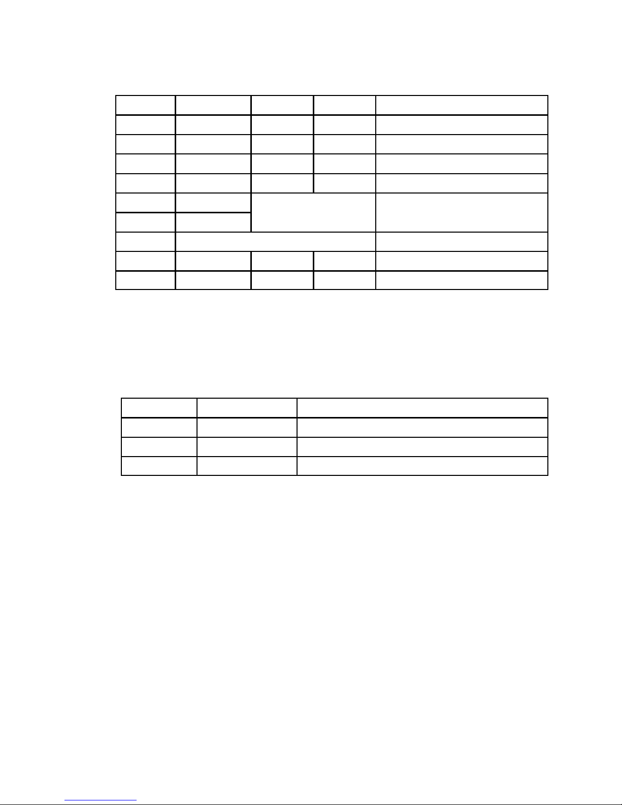
STEP TEST POINT REMARKS
1 IC6 VDD
2 TR5 Pin 4 32.768kHz Clock
3 R1 4.19MHz Microprocessor Clock (every 500ms)
Table 5.4: Decoder Board Test Sequence
Page 60
138 31 26 81115
TAG11335-1
REAR OF LCD DISPLAY
FLEXIBLE
CONNECTOR
SOLDERED
CONNECTIONS
DECODER BOARD
RPR 583
TM1212 Issue 1
Page 5 - 16
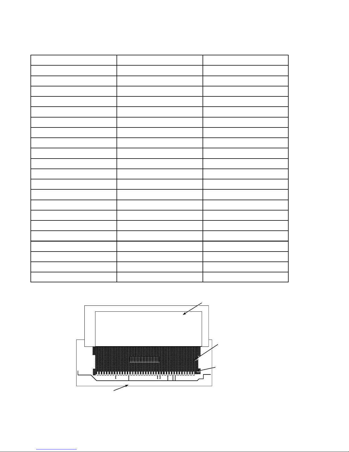
Fig. 5.8: Display Module Connections
CONTACT VOLTAGE REMARKS
6 3.00 VDD
7 3.00 VDD
8 0.0 Ground
9 0.0 Ground
10 0.0 Ground
11 0.0 Ground
12 3.00 VDD
13 3.00 VDD
26 0.0 Ground
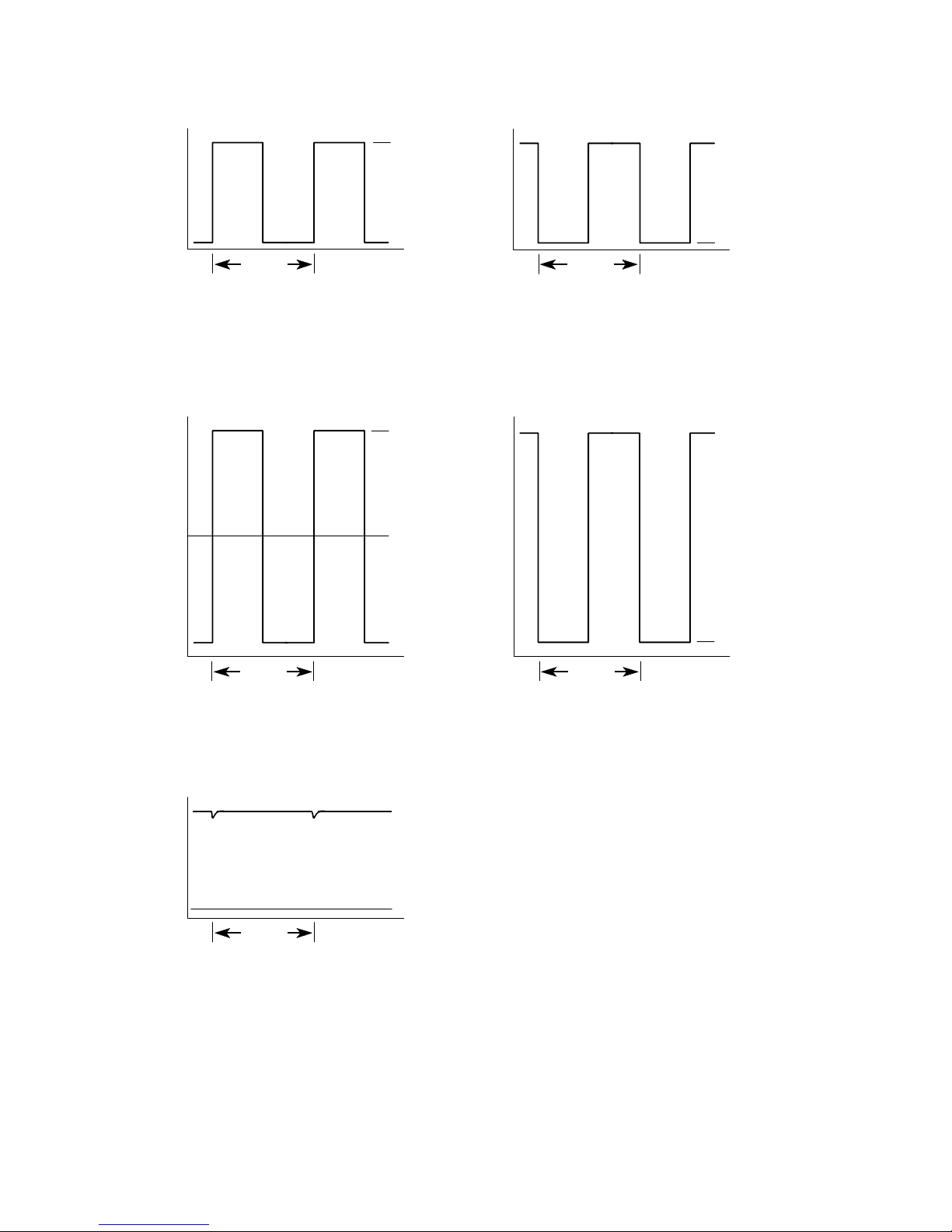
27 1.48dc 3V p-p Cap1+
28 -1.48dc 3V p-p Cap129 0.06dc 6V p-p Cap2+
30 -2.84dc 6V p-p Cap231 -5.7 Vout
32 3.00 VDD
33 0.26 VR
34 -3.09 V5
35 -2.16 V4
36 -1.21 V3
37 1.33 V2
38 2.2 V1
Table 5.5: Display Module Voltages
Page 61
VOLTS
TIME
2.2V
0.19V
4.19MHz WITHIN THE ENVELOPE
4ms
VOLTS
TIME
4ms
TAG11348-1
WAVEFORM AT C26
0V
3V
VOLTS
0V
1.49V
WAVEFORM AT R1/C16
WAVEFORM AT IC3, PIN45
TIME
RPR 583
TM1212 Issue 1 Page 5 - 17
Fig. 5.9: Decoder Board Waveforms
Page 62
0.68ms
TIME
0V
WAVEFORM AT PIN 28
3V p-p
VOLTS
0.68ms
TIME
0V
WAVEFORM AT PIN 32
3V
VOLTS
0.68ms
TIME
WAVEFORM AT PIN 29
0V
6V p-p
VOLTS
TIME
0.68ms
WAVEFORM AT PIN 30
0V
6V p-p
VOLTS
0.68ms
TIME
0V
WAVEFORM AT PIN 27
3V p-p
VOLTS
TAG11334-1
RPR 583
TM1212 Issue 1
Page 5 - 18
Fig 5.10: Display Module Waveforms
Page 63
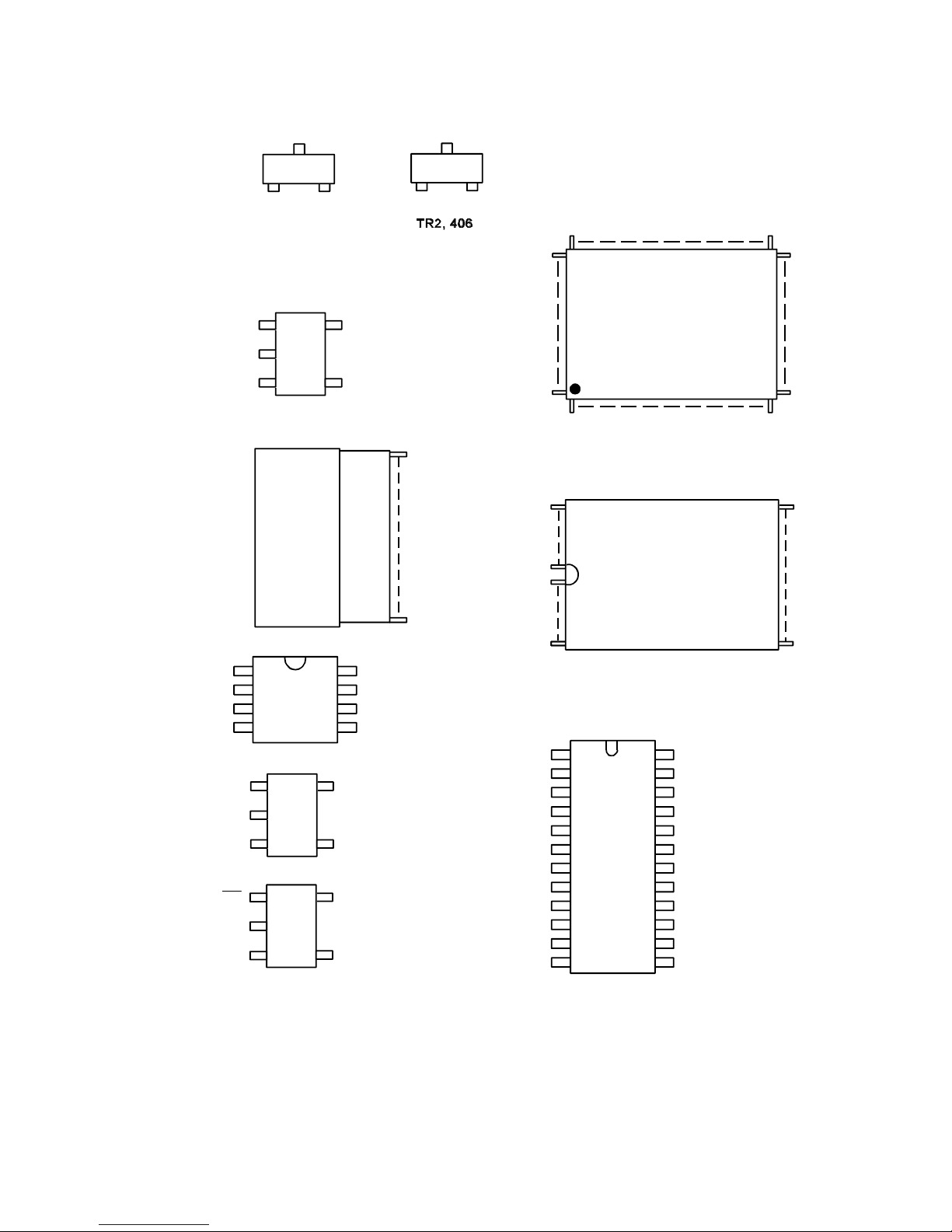
3 (C)
2 (B) 1 (E)
TR1, 3, 4, 6, 7
1
12 13
24
IF IN
OSC BASE
IF DE-COUPLE
QUAD IN
RF IN
GROUND
REG IN
BATTERY ALARM
FSK OUT
POWER SAVE
SHAPING CAP
PRI SHAPING CAP
QUICK CHARGE
FILTER OUT
DET OUT
FILTER IN
OSC EMITT
IF DE-COUPLE
IF OUT
IC401
MIXER OUT
Vcc
REG OUT
RSSI OUT
RSSI IN
TAG11349-1
1
4 5
8
VCC
SDA
A2
IC1
VSS
A0
A1
SCL
NC
EXCEPT FOR THE LCD MODULE,
ALL DEVICES ARE VIEWED FROM ABOVE.
1
16
33
32
48
49
64
17
µP
IC3
7
1
22
28
21
8
IC4
SRAM
Module)
(Rear of
51
1
LCM
1
3
NCOUT
5
4
IC5
Vdd
NC
Vss
Vss
1
3
ON/OFF
NC
V OUT
CONT
5
4
IC6
TR401, 402, 403, 407,
3 (C)
1 (B) 2 (E)
NOT TO SCALE.
408, 410, 414, 415, 416
1
3
NC
A
5
4
TR5
Vdd
Y
Vss
RPR 583
TM1212 Issue 1 Page 5 - 19
Fig. 5.11: Semiconductor Connection Details
Page 64

RPR 583
TM1212 Issue 1
Page 5 - 20
Pin Number Pin Name Description
1 P30 PGM - programming input
2 P31 BEEP - output signal
3 P32 ROM-CE - CGROM (IC2) chip enable€
4 P33 RAM-CE - SRAM (IC4) chip enable
5 P34 LCD-CS - Display chip select
6 P35 µP (IC3) low current mode switch
7 P36 Vibrate Motor - output signal
8 P37 Lamp - output signal
9 VSS Ground
10-12 P40-P42 SW1-SW3 - input signal
13,14,16,17 NC Not Used
15 P45 µP (IC3) low current mode switch
18-23,25-34,38,39 P50-P57,P60-P67,P02,P03 Address lines AD00-AD17
24 VSS Ground
35 RESET µP reset - input signal
36 P00 AREA (No valid data) - input signal
37 P01 ATTN (Valid data) - input signal
40 VDD VDD
41 X2 Xtal oscillator
42 X1 Xtal oscillator
43,46 VPP/IC,AVSS Ground
44 NC Not Used
45 P04/XT1 Clock - input signal
47-54 D00-D07 Data lines
55 AVDD VDD
56 AVR Ground
57 P20 SDO - Data input signal
58 P21 SDI - µP info. to decoder
59 P22 SCK - Data transfer clock
60 WR Display and RAM - Read/write control
61 P24 LOWBAT - output signal
62,63,64 P25,P26,P27 Serial Data input from EEPROM (IC1)
Table 5.6: IC3 Microprocessor Pin Connections
Page 65

RPR 583
TM1212 Issue 1 Page 5 - 21
Pin Number Pin Name Description
1 A14 Address line AD14
2 A12 Address line AD12
3 A7 Address line AD07
4 A6 Address line AD06
5 A5 Address line AD05
6 A4 Address line AD04
7 A3 Address line AD03
8 A2 Address line AD02
9 A1 Address line AD01
10 A0 Address line AD00
11 D0 Data line D00
12 D1 Data line D01
13 D2 Data line D02
14 VSS Ground
15 D3 Data line D03
16 D4 Data line D04
17 D5 Data line D05
18 D6 Data line D06
19 D7 Data line D07
20 CE RAM-CE - chip enable input
21 A10 Address lineAD10
22 OE Ground
23 A11 Address line AD11
24 A9 Address line AD09
25 A8 Address line AD08
26 A13 Address line AD13
27 WE WR - RAM read/write control
28 VDD VDD
Table 5.7: IC4 RAM Pin Connections
Page 66

RPR 583
TM1212 Issue 1
Page 5 - 22
Pin Number Pin Name Description
1-4 NC Not Used
5 RESET Reset - input signal
6 VDD VDD
7 PS VDD
8 C86 Ground
9 VSS Ground
10 T2 Ground
11 T1 Ground
12 SCL VDD
13 SI VDD
14 CS1 LCD-CS - chip select
15 A0 AD16 - display address input signal
16 WR WR - LCD write enable input signal
17 RD AD17 - read enable input signal
18-25 D0-D7 D00-D07 - Data lines
26 VSS Ground
27 CAP1+ DC/DC voltage converter capacitor 1
28 CAP1- DC/DC voltage converter capacitor 1
29 CAP2+ DC/DC voltage converter capacitor 2
30 CAP2- DC/DC voltage converter capacitor 2
31 VOUT DC/DC voltage converter output
32 VDD VDD
33 VR Voltage adjustment terminal
34-38 V5-V1 LCD driver supply voltages
Table 5.8: LCD Display Pin Connections
Page 67
SIGNAL
COUNTER
HF
GENERATOR
SINAD
P671A
OSCILLO-
SCOPE
METER
AUDIO OUT
1kHz MODULATION
INPUT
455kHz
RF IN
10dB
ATTENUATOR
RPR 583
TM1212 Issue 1 Page 5 - 23
Fig. 5.12: Radio Alignment Test Equipment
5.8 RADIO ALIGNMENT PROCEDURE
5.8.1 Preparation
a) Remove the Board Assembly from the Case (see paragraph 5.5.2).
b) Install a 0 ohm resistor or a shorting link in the position for R456, to disable the
BEC.
c) Disable the AGC circuit by connecting TP403 to 0 volts. Alternatively, lift R409.
5.8.2 Alignment Procedure
a) Configure the test equipment as shown in Figure 5.12. Set the signal generator
to the channel frequency with an output of -10dBm.
b) Put the Board Assembly in the tray of the P671A Alignment Jig and connect the
frequency counter probe to TP405. Adjust CV405 to give a reading of
455kHz ±200Hz at the frequency counter.
c) Adjust CV406 for maximum amplitude of the 455kHz signal on the oscilloscope.
A minimum of 500 millivolts should be achieved.
d) Remove the AGC disable and assemble the Board Assembly in the case.
Remove the right hand label from the case back to expose the aerial trimmer.
Page 68
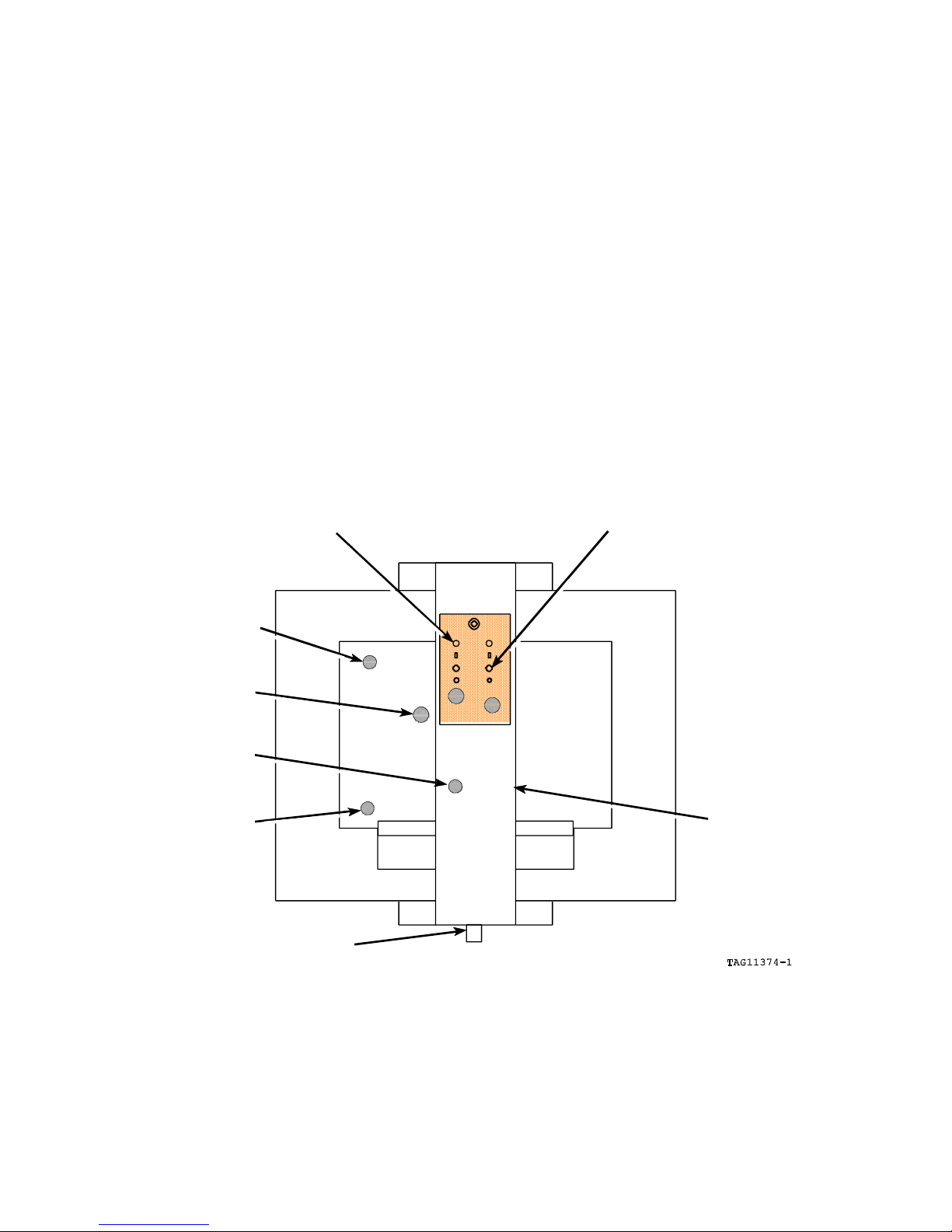
ARM
ARM LOCK
CV404
CV406
CV407
ALIGNMENT PINS PROGRAMMING PINS
CV405
RPR 583
TM1212 Issue 1
Page 5 - 24
Fig. 5.13: P671A Showing the Tuning Points
e) Put a known good battery in the unit (but leave the battery door off). Put the unit
in the P671A jig, fold the jig arm over the unit and lock the arm in position.
f) Connect the SINAD meter to the alignment pins on the P671A (refer to
Figure 5.13)
g) Set the modulation to 1kHz at a deviation of 3 kHz and switch it ON. Adjust
CV404 to give 12dB sinad with minimum RF input. A reading of -98dB should
be achieved.
NOTE: Do not disturb the aerial during the next operation.
h) Carefully remove the Board Assembly from the case. Remove the BEC disable
0 ohm resistor or the shorting link from R456 position. Carefully assemble the
Board Assembly in the case and put a new label on the case back to cover the
aerial trimmer access hole.
Page 69
GENERATOR
SIGNAL
PC
RF IN
10dB
ATTENUATOR
P645
TAG11331-1
DATA
NOTE: THE DISTANCE BETWEEN THE
PC AND THE P671A MUST BE
GREATER THAN TWO METRES
RPR 583
TM1212 Issue 1 Page 5 - 25
Fig. 5.14: Configuration for Coarse Sensitivity Measurement
5.8.3 Pager Sensitivity Measurement (Coarse)
To determine the pager sensitivity, configure the test equipment as shown in
Figure 5.14 and do the procedure given in sub-paragraphs a) through e).
NOTE: This is only an indication of sensitivity, which is dependant on the unit under
test being in a noise free environment.
a) Set the signal generator to the channel frequency, at a deviation of 4.5kHz and
an output level of -85dBm.
b) Install a known good battery in the pager and switch it ON.
c) Put the pager in the P671A and send a sensitivity call from the P645. Increase
the signal generator output level, if necessary, to obtain a correctly received
call.
d) Reduce the RF level in 1dB steps until the pager receives less than three calls
in five.
e) Increase the RF level in 1dB steps until five consecutive calls are received. An
output level of -98dBm should be achieved.
5.8.4 Pager Sensitivity Measurement (Fine)
Configure the equipment as described in paragraph 5.8.3 but connect a P800 TEM
cell instead of the P671A. Follow the steps given in the TEM Cell Instructions for the
IEC method. Place the pager in the polystyrene block (refer to Figure 5.15)
positioned centrally in the TEM Cell, with the display facing the input end. A level of
-103dBm or better should be achieved.
Page 70
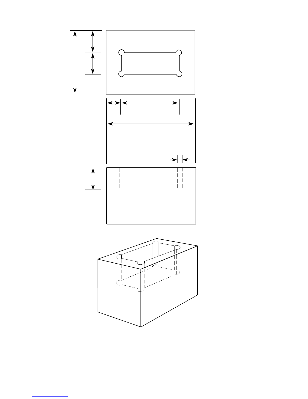
TAG11124-1
+
++
60mm
14mm
52mm
20mm
20mm
+
20mm
ø 5mm
80mm
RPR 583
TM1212 Issue 1
Page 5 - 26
Fig. 5.15: Polystyrene Block for TEM Cell Test - Dimensions
Page 71
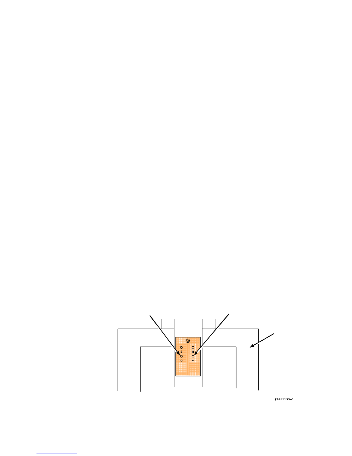
CONNECT THE BLUE
WIRE TO THIS PIN
CONNECT THE BROWN
WIRE TO THIS PIN
P671A
RPR 583
TM1212 Issue 1 Page 5 - 27
Fig. 5.16: Programming Lead Connections
5.9 PROGRAMMING
5.9.1 General
The pager contains an EEPROM which holds unique data. The data may be altered
as shown in the following paragraphs.
5.9.2 Equipment
The following equipment is required:
! P671A Alignment Jig
! P672A Programming Software
! Programming Cable
! IBM PC or equivalent
5.9.3 Procedure
Program the receiver as follows:
a) Remove the Battery Door from the Case Back.
b) Put the unit face down in the tray of the P671A, lower the arm over the unit and
lock the arm in position.
c) Use the Programming Cable to connect the programming pins of the P671A to
the PC serial port. Refer to Figure 5.16 and connect the correct coloured wire
to each programming pin.
d) Read the ‘Read me’ file contained in the relevant programming software. The
‘Read me’ file describes how to use the programming facility.
Page 72

RPR 583
TM1212 Issue 1
Page 5 - 28
INTENTIONALLY BLANK
Page 73

RPR 583
TM1212 Issue 1 Page 6 - 1
SECTION 6
SPARE PARTS LIST
CONTENTS: Page
ASSEMBLIES 6 - 2
Modules 6 - 2
Case Parts 6 - 2
Miscellaneous 6 - 2
Labels - Multitone, Standard 6 - 2
RADIO BOARD (PCB 3061- 5617) 6 - 3
Capacitors 6 - 3
Banded Capacitors 6 - 4
Crystals & Filters 6 - 4
Banded Crystals 6 - 5
Diodes 6 - 5
Inductors 6 - 5
Banded Inductors 6 - 5
Resistors 6 - 6
Banded Resistors 6 - 6
Semiconductors 6 - 7
Banded Semiconductor 6 - 7
Miscellaneous 6 - 7
DECODER ASSEMBLY (PCB 3061- 5946) 6 - 8
Capacitors 6 - 8
Diodes 6 - 8
Inductors 6 - 8
Resistors 6 - 8
Semiconductors 6 - 9
Miscellaneous 6 - 9
Page 74

RPR 583
TM1212 Issue 1Page 6 - 2
CAUTION
STATIC SENSITIVE DEVICES ARE USED WITHIN THIS EQUIPMENT. CARE MUST BE
TAKEN WHEN HANDLING THESE DEVICES AS THEY MAY BE DAMAGED BY HIGH
LEVELS OF STATIC ELECTRICITY.
ITEM/CIRCUIT
REFERENCE
DESCRIPTION PART No.
ASSEMBLIES
Modules
RPR580 DECODER, LATIN WITH DISPLAY 0201-1002-LATIN
Case Parts
ASSEMBLY CASE FRONT, DARK BEIGE Style 1 0801-0292
ASSEMBLY CASE FRONT, DARK BEIGE Style 2 0801-0304
ASSEMBLY CASE BACK, BLACK 0861-5734
BATTERY DOOR 0801-0160
WINDOW MULTITONE style 1 0961-5986
WINDOW MULTITONE style 2 0961-6093
GASKET DISPLAY SEAL 2561-5007
Miscellaneous
BATTERY CONTACT, POSITIVE 7361-4862
BATTERY CONTACT, NEGATIVE, SPRING 7361-4861
BATTERY ALKALINE, AAA 5601-0006
HOLSTER TLA, BLACK 0801-0345
LANYARD ELASTICATED 7961-5055
SCREW 2.2mm X 6mm PAN SELFTAP SILV (2 OFF) 8216-2296
Labels - Multitone, Standard
LABEL SET RPR 580 SERIES 2061-5736
Page 75

RPR 583
TM1212 Issue 1 Page 6 - 3
ITEM/CIRCUIT
REFERENCE
DESCRIPTION PART No.
RADIO BOARD (PCB 3061- 5617)
Capacitors
C401 CAP CHIP 8p2 0.25p 50V 3301-0012
C402 CAP CHIP 1u0 -20/+80% 16V 3301-0277
C403,412,416,484 CAP CHIP 10n 10% 50V 3327-0025
C404,406,414,418,453,
457,466,478 CAP CHIP 100p 5% 50V 3326-0027
C407,408 CAP, CHIP 3p9 0p25 50V 3326-0010
C409,413,419,423,450,452,
471,473,477,479,480 CAP CHIP 100n 10% 16V 3332-0014
C417,426 CAP CHIP 33p 5% 50V 3326-0021
C420 CAP CHIP 220n 10% 16V 3301-0337
C432,440,447 CAP CHIP 4p7 0p25 50V 3326-0011
C436,490 CAP CHIP 22u 20% 4V0 3412-0005
C437 CAP CHIP 330n 16V 0805 3301-0339
C441 CAP CHIP 1p8 0.25p 50V 3301-0004
C445 CAP CHIP 1p2 0p25 50V 3326-0004
C448 CAP CHIP 3n3 10% 50V 3327-0019
C449 CAP CHIP 22n +80-20% 50V 3328-0009
C451 CAP CHIP 30p 2% 50V 3336-0018
C455 CAP CHIP 10p 0p5 50V 3326-0015
C462,465 CAP CHIP 2p2 0p25 50V 3326-0007
C472,474 CAP CHIP 1n0 10% 50V 3327-0013
C483 CAP CHIP 560p 3326-0036
C486 CAP CHIP 33n 10% 16V 3332-0008
C492 CAP CHIP 4.7u 6.3V 3412-0104
CV404,405,406,407 CAP SMD CER TRIMMER 3p0-10p 3508-0004
Page 76
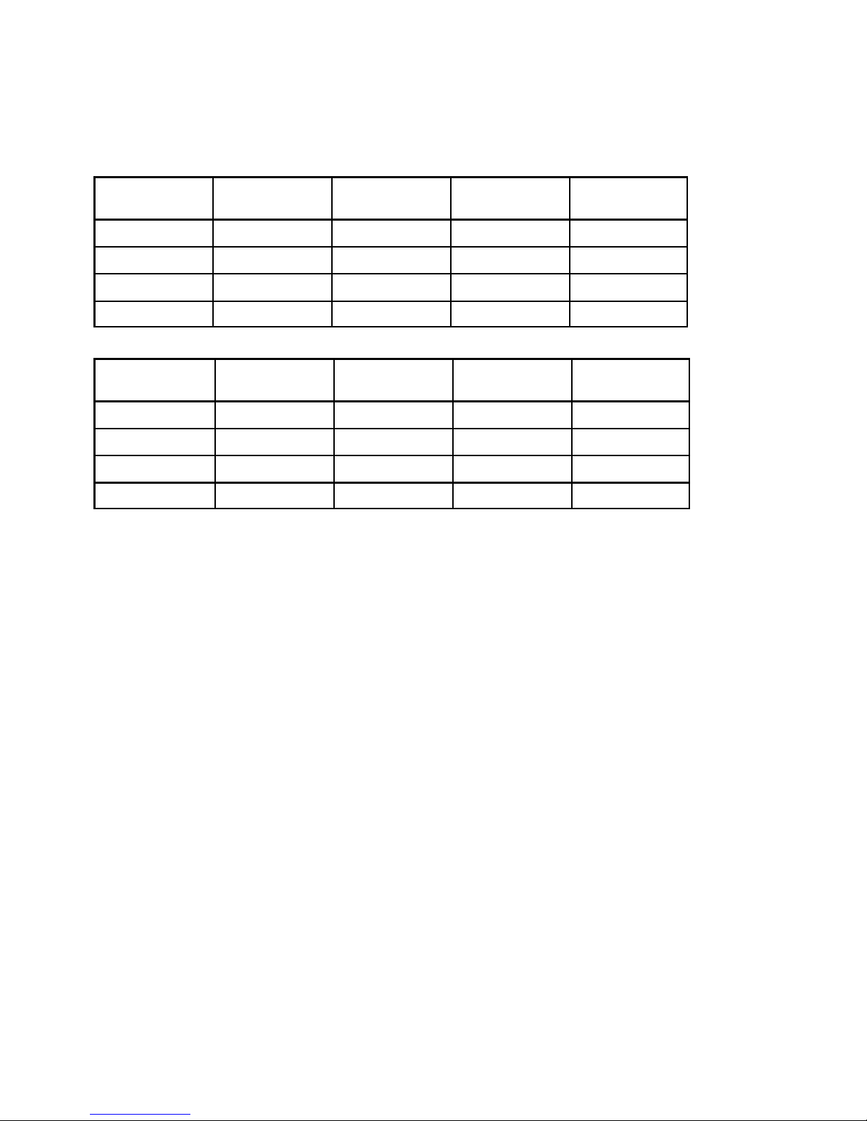
RPR 583
TM1212 Issue 1Page 6 - 4
ITEM/CIRCUIT
REFERENCE
DESCRIPTION PART No.
Banded Capacitors
BAND 1 BAND 2 BAND 3 BAND 4
430-434.999MHz 435-439.999MHz 440-443.999MHz 444-446.999MHz
C428 13p 13p 13p 13p
C459 11p 11p 11p 10p
C463 13p 13p 12p 12p
C464 12p 12p 12p 12p
BAND 5 BAND 6 BAND 7 BAND 8
447-450.999MHz 451-456.999MHz 457-462.999MHz 463-469.999MHz
C428 12p 12p 12p 11p
C459 10p 10p 8p2 8p2
C463 11p 11p 10p 10p
C464 11p 11p 11p 10p
DESCRIPTION PART No.
CAP CHIP 8p2 0p5 50V 3326-0014
CAP CHIP 10p 0p5 50V 3326-0015
CAP CHIP 11p 2% 50V 3336-0013
CAP CHIP 12p 2% 50V 3336-0016
CAP CHIP 13p 2% 50V 3336-0014
Crystals & Filters
FL401 FILTER 45MHz 4001-0024
FL402,403 CERAMIC IF FILTER 4018-0002
FL404 FILTER CHIP 4003-0005
XL402 XTAL (FIRST LOCAL OSCILLATOR) 3955-*
*QUOTE THE CHANNEL FREQUENCY TO 6 DECIMAL PLACES
Page 77
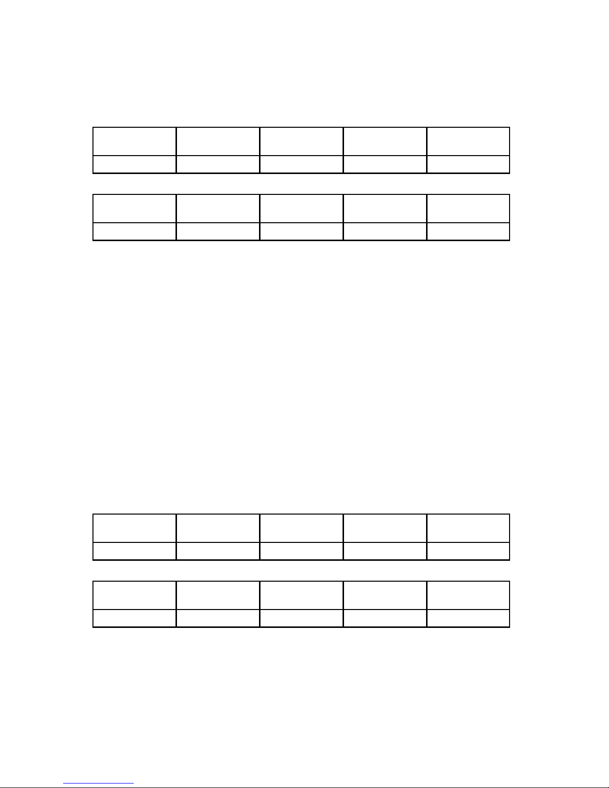
RPR 583
TM1212 Issue 1 Page 6 - 5
ITEM/CIRCUIT
REFERENCE
DESCRIPTION PART No.
Banded Crystals
BAND 1 BAND 2 BAND 3 BAND 4
430-434.999MHz 435-439.999MHz 440-443.999MHz 444-446.999MHz
XL401 44.545MHz 44.545MHz 44.545MHz 45.455MHz
BAND 5 BAND 6 BAND 7 BAND 8
447-450.999MHz 451-456.999MHz 457-462.999MHz 463-469.999MHz
XL401 44.545MHz 44.545MHz 44.545MHz 44.545MHz
DESCRIPTION PART No.
XTAL , SECOND L.O., 44.545MHz 3915-0015
XTAL , SECOND L.O., 45.455MHz 3915-0014
Diodes
D401 DIODE SWITCHING 3703-0047
Inductors
L406 IND CHIP 390n 4111-0045
L407 IND CHIP 15n 5% 4103-0244
L408 IND CHIP 270n 5% 4103-0264
L409 IND CHIP 470n 5% 4103-0270
L411,413,415 IND CHIP 8n2 5% 4118-0023
L412 IND CHIP 1u0 5% 4103-0278
L414 INDUCTOR 100u 10% 4114-0069
Banded Inductors
BAND 1 BAND 2 BAND 3 BAND 4
430-434.999MHz 435-439.999MHz 440-443.999MHz 444-446.999MHz
L401 15n 15n 12n 12n
BAND 5 BAND 6 BAND 7 BAND 8
447-450.999MHz 451-456.999MHz 457-462.999MHz 463-469.999MHz
L401 12n 12n 12n 12n
DESCRIPTION PART No.
IND CHIP 15n 5% 4103-0244
IND CHIP 12n 5% 4103-0243
Page 78
RPR 583
TM1212 Issue 1Page 6 - 6
ITEM/CIRCUIT
REFERENCE
DESCRIPTION PART No.
Resistors
R401 RES CHIP 56S 5% 62m5W 3115-0044
R402 RES CHIP 10k 5% 62m5W 3115-0098
R403,408,439,448,470 RES CHIP 100S 5% 62m5W 3115-0050
R404,446,464 RES CHIP 1k0 5% 62m5W 3115-0074
R405 RES CHIP 18k 5% 62m5W 3115-0104
R407,416 RES CHIP 68k0 5% 62m5W 3115-0118
R409,443 RES CHIP 4k7 5% 62m5W 3115-0090
R410,463 RES CHIP 33k 5% 62m5W 3115-0110
R411 RES CHIP 22k 5% 62m5W 3115-0106
R418 RES CHIP 47k 5% 62m5W 3115-0114
R425,428,429 RES CHIP 82k 5% 62m5W 3115-0120
R430 RES CHIP 0S 5% 62m5W 3115-0001
R433 RES CHIP 1k2 5% 62m5W 3115-0076
R434 RES CHIP 15k 5% 62m5W 3115-0102
R438,445 RES CHIP 680S 5% 62m5W 3115-0070
R440,452 RES CHIP 220S 5% 62m5W 3115-0058
R444,457,471 RES CHIP 100k 5% 62m5W 3115-0122
R449 RES CHIP 56S 5% 0.125W 3101-0116
R450 RES CHIP 10S 5% 62m5W 3115-0026
R451 RES CHIP 180S 5% 62m5W 3115-0056
Banded Resistors
BAND 1 BAND 2 BAND 3 BAND 4
430-434.999MHz 435-439.999MHz 440-443.999MHz 444-446.999MHz
R412 1k0 1k0 1k0 N/F
R465 N/F N/F N/F 33k
BAND 5 BAND 6 BAND 7 BAND 8
447-450.999MHz 451-456.999MHz 457-462.999MHz 463-469.999MHz
R412 1k0 1k0 1k0 1k0
R465 N/F N/F N/F N/F
DESCRIPTION PART No.
RES CHIP 1k0 5% 62m5W 3115-0074
RES CHIP 33k 5% 62m5W 3115-0110
Page 79
RPR 583
TM1212 Issue 1 Page 6 - 7
ITEM/CIRCUIT
REFERENCE
DESCRIPTION PART No.
Semiconductors
IC401 IC TK14590V 3825-0002
TR401,403,410 TRANS CHIP NE85619 3601-0013
TR 402,414 TRANS CHIP NPN 2SC4726-TL 3602-0052
TR406 TRANS CHIP BC808-40W 3602-0058
TR407 TRANS CHIP 2SA1774 3602-0049
TR415 TRANS CHIP DTC115TUA 3611-0004
TR416 TRANS CHIP 2SD1757KS 3602-0038
Banded Semiconductor
BAND 1 BAND 2 BAND 3 BAND 4
430-434.999MHz 435-439.999MHz 440-443.999MHz 444-446.999MHz
TR408 N/F N/F N/F DTC115TUA
BAND 5 BAND 6 BAND 7 BAND 8
447-450.999MHz 451-456.999MHz 457-462.999MHz 463-469.999MHz
TR408 N/F N/F N/F N/F
DESCRIPTION PART No.
TRANS CHIP DTC115TUA 3611-0004
Miscellaneous
AE401 AERIAL SECTION OUTER HALF 5561-4982
AE402 AERIAL SECTION INNER HALF 5561-4983
PL401 HEADER DUAL ROW POST 14-WAY 4332-0002
SP401 TRANSDUCER 5004-0007
Page 80

RPR 583
TM1212 Issue 1Page 6 - 8
ITEM/CIRCUIT
REFERENCE
DESCRIPTION PART No.
DECODER ASSEMBLY (PCB 3061- 5946)
Capacitors
C3,6,8,9,10,11,14,19,20,21,
22,23,24,25 CAP CHIP 100n 10% 16V 3332-0014
C4 CAP CHIP 68p 5% 50V 3326-0025
C5 CAP CHIP 15p 5% 50V 3326-0017
C7 CAP CHIP 10u 20% 6V3 3412-0106
C12,15 CAP CHIP 47u 20% 6V3 3412-0110
C13 CAP CHIP 100p 5% 50V 3326-0027
C16,26 CAP CHIP 27p 5% 50V 3326-0020
C17,18 CAP CHIP 1u0 -20/+80% 16V 3301-0277
Diodes
D2 DIODE RB715F 3710-0005
Inductors
L2 IND CHIP 100u 4119-0001
Resistors
R1,9 RES CHIP 1k0 5% 62m5W 3115-0074
R6,7,17,20 RES CHIP 10k 5% 62m5W 3115-0098
R8 RES CHIP 47S 5% 62m5W 3115-0042
R10,14,18,19 RES CHIP 100k 5% 62m5W 3115-0122
R11 RES CHIP 470k 2% 62m5W 3118-0138
R12 RES CHIP 150k 5% 62m5W 3115-0126
R13 RES CHIP 680k 5% 62m5W 3115-0142
R15,16 RES CHIP 220S 5% 62m5W 3115-0058
R21 RES CHIP 10M 0603 5% 62m5W 3115-0170
Page 81

RPR 583
TM1212 Issue 1 Page 6 - 9
ITEM/CIRCUIT
REFERENCE
DESCRIPTION PART No.
Semiconductors
IC1 IC 512X8 EPROM 3818-0006
IC3 MICROPROCESSOR, OTP RPR580 0501-0215
IC4 IC 32KX8 SRAM 3821-0009
IC5 IC VOLTAGE DETECTOR 2V0 6003-0011
IC6 IC VOLTAGE CONVERTER 3V0 6004-0005
TR1,3,6 CHIP TRANS DTC115TUA 3611-0004
TR2 TRANS PNP, BC808-40W 3602-0058
TR4 TRANS 2SD1757KS 3602-0038
TR5 IC BU4S584F 3837-0004
TR7 TRANS NPN, 2SC4617 3602-0050
Miscellaneous
BAT 2 BAT POLY CAP PAS621L-VL5 3331-0002
LCM DISPLAY LCD, TLA SEIKO 5206-0020
LP1 LAMP, BACKLIGHT 5202-0007
M1 MOTOR VIBRATE, 1.3V 6502-0008
SK1 HEADER DUAL ROW RECEPT 14-WAY SMD 4449-0002
SW1,2,3 SWITCH SMD KSR221G 4202-0026
XL1 CRYSTAL 4.194304MHz SMD 3915-0019
XL2 CRYSTAL, CLOCK 32.768kHz +/-20ppm SMD 3922-0014
BEZEL, SEIKO 0861-5217
DIFFUSER, MOULDED 0861-5661
RUBBER SPACER, MODIFIED RPR583 0861-6099
Page 82

RPR 583
TM1212 Issue 1Page 6 - 10
INTENTIONALLY BLANK
Page 83

RPR 583
TM1212 Issue 1 Page 7 - 1
SECTION 7
DIAGRAMS
CONTENTS: Source Drawing Page
7.1 Radio Board (PCB 3061-5617 Iss. 1) 2961-5618 Iss. 1 7 - 3/4
Circuit Diagram (Sheet 1 of 2)
7.2 Radio Board (PCB 3061-5617 Iss. 1) 2961-5018 Iss. 1 7 - 5/6
Circuit Diagram (Sheet 2 of 2)
7.3 Radio Board (PCB 3061-5617 Iss. 1) 0261-5616 Iss. 1 7 - 7/8
Component Layout - Side 1
7.4 Radio Board (PCB 3061-5617 Iss. 1) 0261-5616 Iss. 1 7 - 9/10
Component Layout - Side 2
7.5 Decoder Board (PCB 3061-5946 Iss. 1) 2961-5947 Iss. 1 7 - 11/12
Circuit Diagram
7.6 Decoder Board (PCB 3061-5946 Iss. 1) 0261-5945 Iss. 1 7 - 13/14
Component Layout - Side 1
7.7 Decoder Board (PCB 3061-5946 Iss. 1) 0261-5945 Iss. 1 7 - 15/16
Component Layout - Side 2
Page 84

RPR 583
TM1212 Issue 1Page 7 - 2
INTENTIONALLY BLANK
Page 85
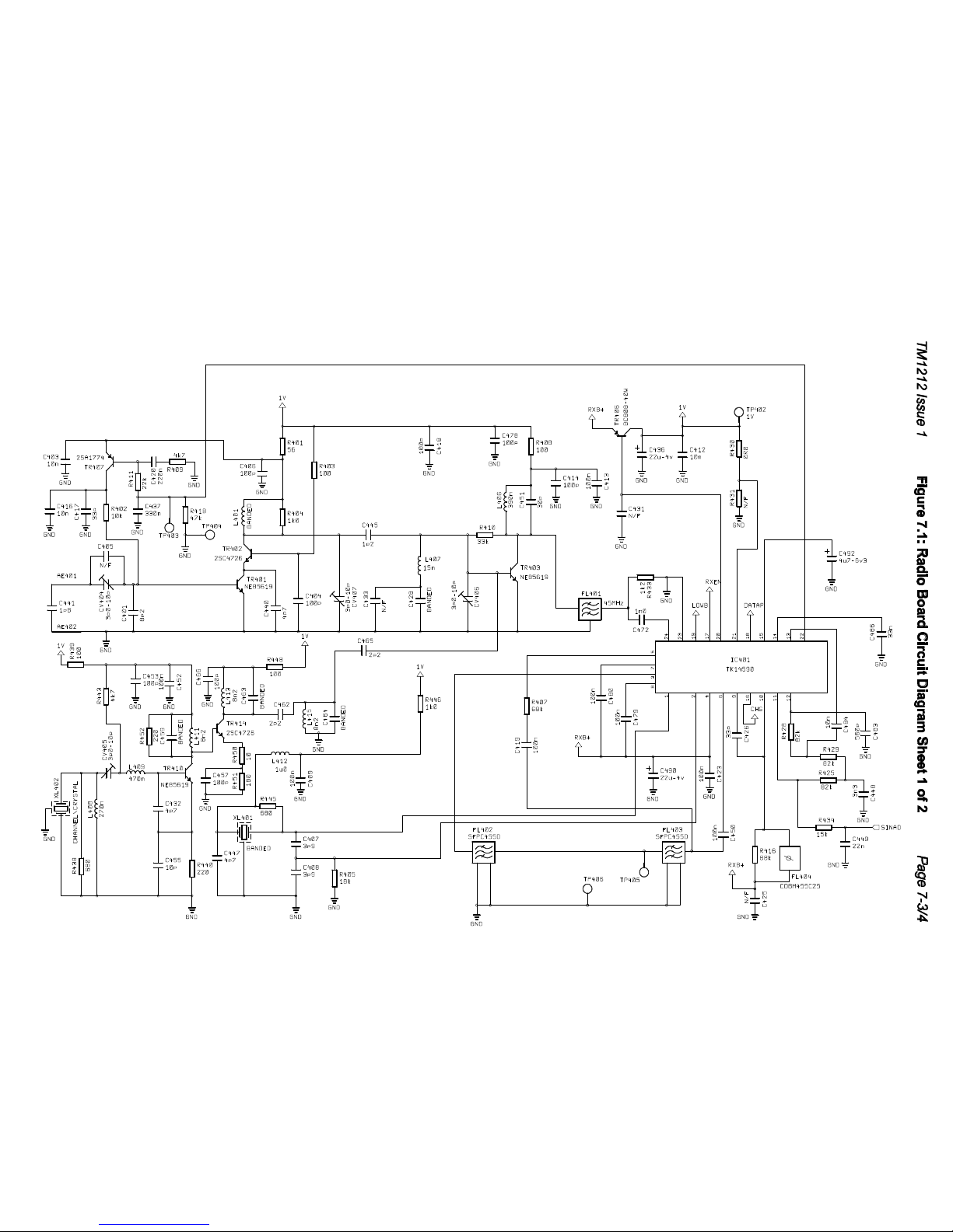
Page 86
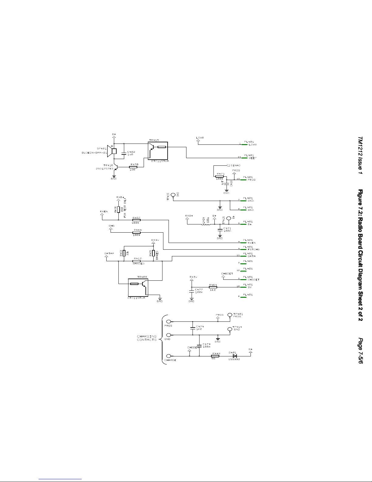
Page 87
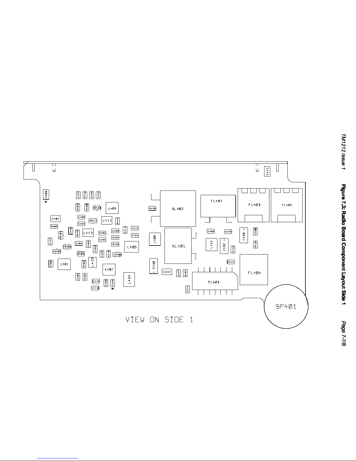
Page 88
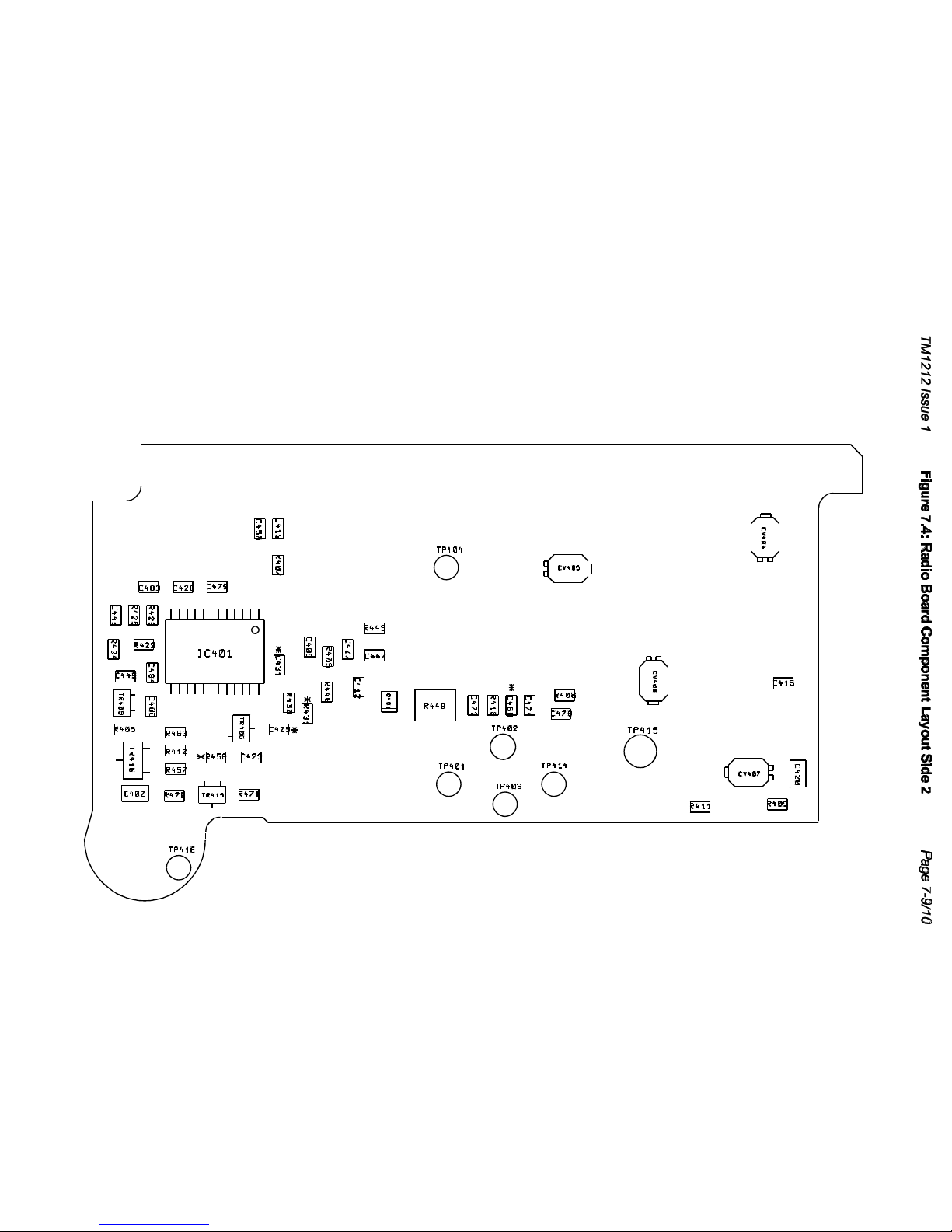
Page 89
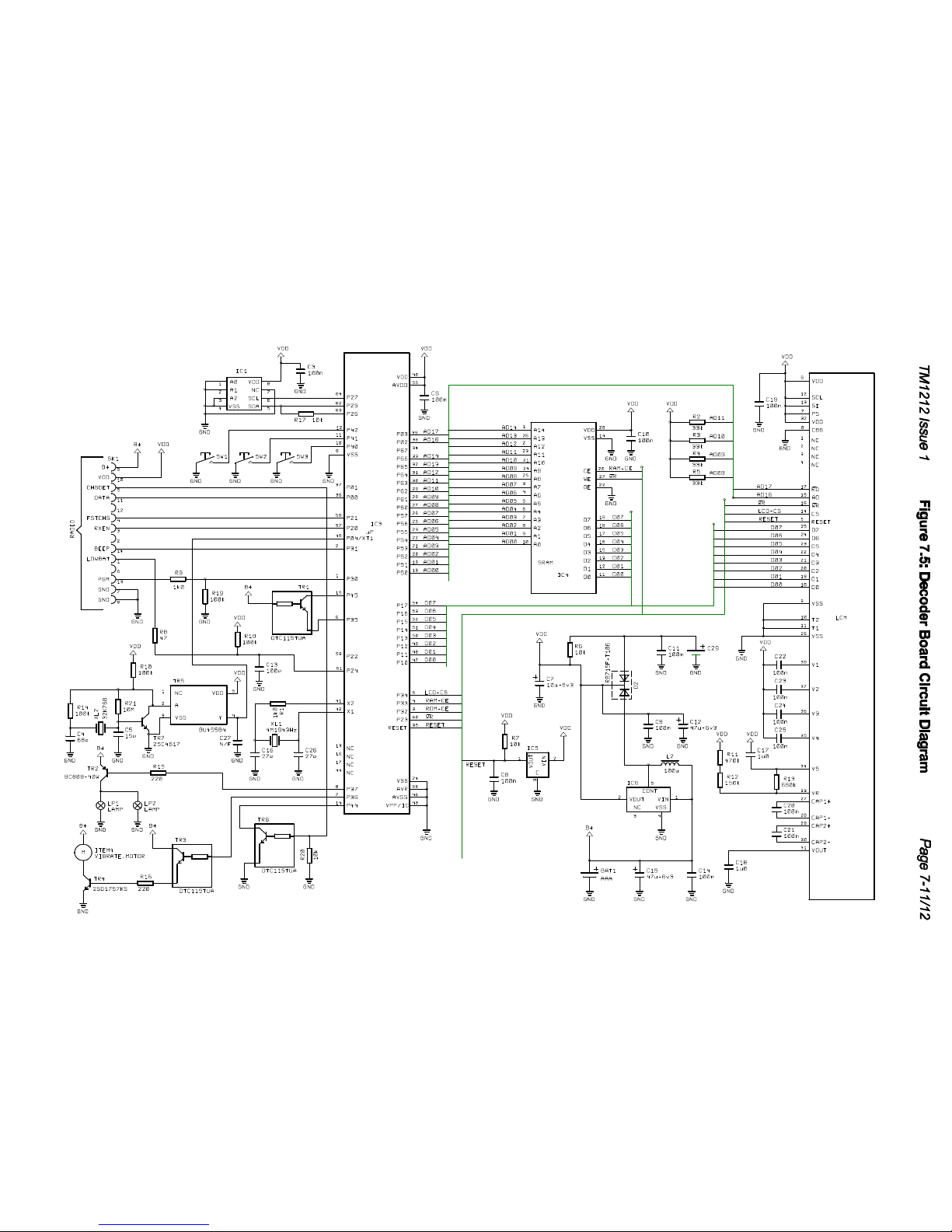
Page 90
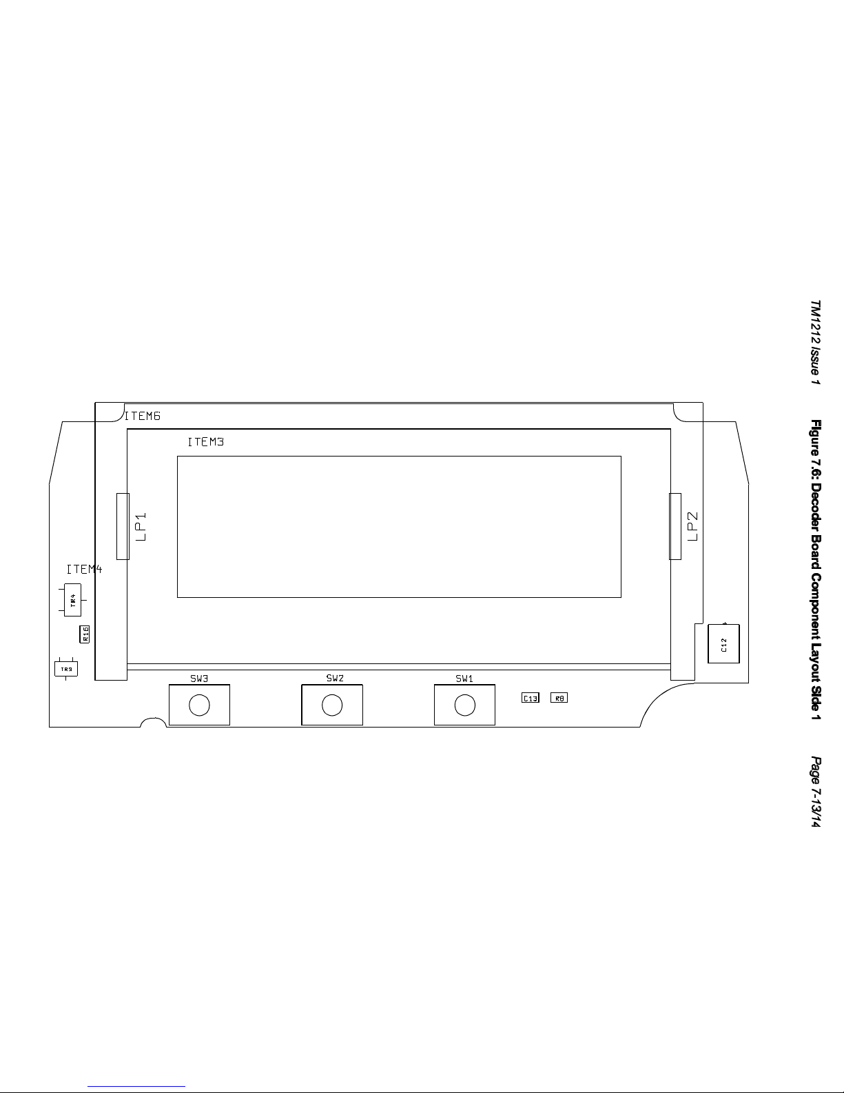
Page 91
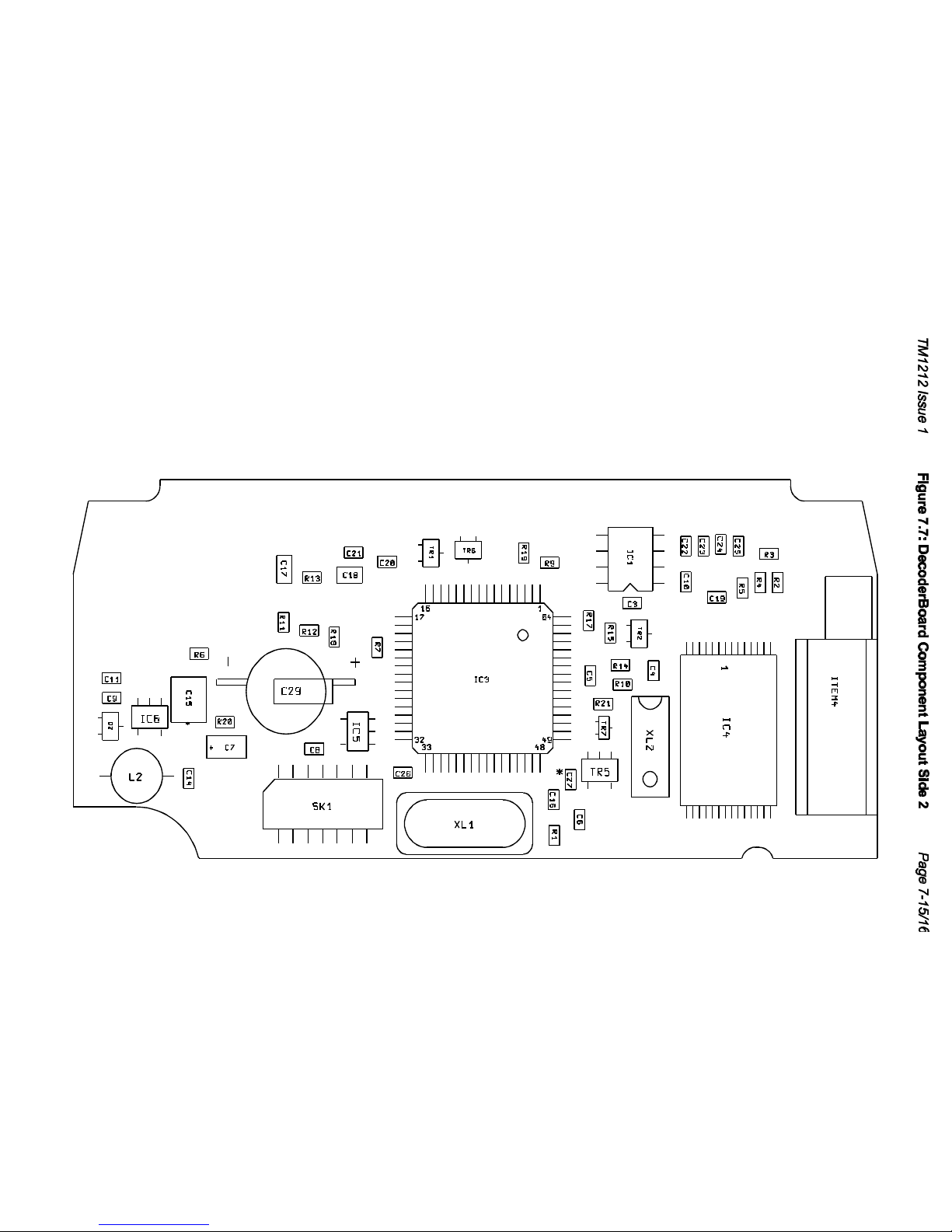
 Loading...