

Page 1
FCC-B Radio Frequency Interference Statement
This equipment has been tested and found to comply with the limits for a class B digital device, pursuant to part
15 of the FCC rules. These limits are designed to provide reasonable protection against harmful interference
when the equipment is operated in a commercial environment. This equipment generates, uses and can
radiate radio frequency energy and, if not installed and used in accordance with the instruction manual, may
cause harmful interference to radio communications. Operation of this equipment in a residential area is likely
to cause harmful interference, in which case the user will be required to correct the interference at his own
expense.
Notice 1
The changes or modifications not expressly approved by the party responsible for compliance could void the
user’s authority to operate the equipment.
Notice 2
Shielded interface cables and A.C. power cord, if any, must be used in order to comply with the emission limits.
VOIR LA NOTICE D’NSTALLATION AVANT DE RACCORDER AU RESEAU.
Micro-Star International
MS-7095
This device complies with Part 15 of the FCC Rules. Operation is subject to the following two conditions:
(1) this device may not cause harmful interference, and
(2) this device must accept any interference received, including interference that may cause undesired
operation
G52-M7095X1
i
Page 2

Copyright Notice
The material in this document is the intellectual property of MICRO-STAR INTERNATIONAL. We take every
care in the preparation of this document, but no guarantee is given as to the correctness of its contents. Our
products are under continual improvement and we reserve the right to make changes without notice.
Trademarks
All trademarks are the properties of their respective owners.
AMD, Athlon™ Athlon™XP, Thoroughbred™ and Duron™ are registered trademarks of AMD Corporation.
Intel® and Pentium® are registered trademarks of Intel Corporation.
PS/2 and OS® 2 are registered trademarks of International Business Machines Corporation.
Microsoft® is a registered trademark of Microsoft Corporation. Windows® 98/2000/NT/XP are registered
trademarks of Microsoft Corporation.
NVIDIA, the NVIDIA logo, DualNet, and nForce are registered trademarks or trademarks of NVIDIA
Corporation in the United States and/or other countries.
Netware® is a registered trademark of Novell, Inc.
Award® is a registered trademark of Phoenix Technologies Ltd.
AMI® is a registered trademark of American Megatrends Inc.
Kensington and MicroSaver are registered trademarks of the Kensington Technology Group.
PCMCIA and CardBus are registered trademarks of the Personal Computer Memory Card International
Association.
Revision History
Revision Revision History Date
V1.0 First released of Multi-language version for PCB 1.x October 2004
with chipsets VIA® VT8751A (P4M266A) & VT8237 (R)
ii
Page 3

Safety Instructions
1. Always read the safety instructions carefully.
2. Keep this User Manual for future reference.
3. Keep this equipment away from humidity.
4. Lay this equipment on a reliable flat surface before setting it up.
5. The openings on the enclosure are for air convection hence protects the equipment from overheating. Do
not cover the openings.
6. Make sure the voltage of the power source and adjust properly 110/220V before connecting the equipment
to the power inlet.
7. Place the power cord such a way that people can not step on it. Do not place anything over the power
cord.
8. Always Unplug the Power Cord before inserting any add-on card or module.
9. All cautions and warnings on the equipment should be noted.
10. Never pour any liquid into the opening that could damage or cause electrical shock.
11. If any of the following situations arises, get the equipment checked by a service personnel:
- The power cord or plug is damaged.
- Liquid has penetrated into the equipment.
- The equipment has been exposed to moisture.
- The equipment does not work well or you can not get it work according to User Manual.
- The equipment has dropped and damaged.
- The equipment has obvious sign of breakage.
12. Do not leave this equipment in an environment unconditioned, storage temperature above 60° C (140°F),
it may damage the equipment.
CAUTION: Danger of explosion if battery is incorrectly replaced. Replace only
with the same or equivalent type recommended by the manufacturer.
iii
Page 4

Table of Content
English.....................................................................1
Deutsch....................................................................15
Français...................................................................31
简体中文 ...................................................................45
繁體中文 ...................................................................59
日本語.......................................................................73
iv
Page 5
Introduction
Thank you for choosing the P4MAM2-V Series (MS-7095 v1.X) micro ATX mainboard. The
P4MAM2-V Series is based on VIA ® VT8751A (P4M266A) & VT8237(R) chipsets for optimal
system efficiency. Designed to fit the advanced Intel ® Pentium ® 4/Celeron(D) processors in
478 pin package, the P4MAM2-V Series delivers a high performance and professional desktop
platform solution.
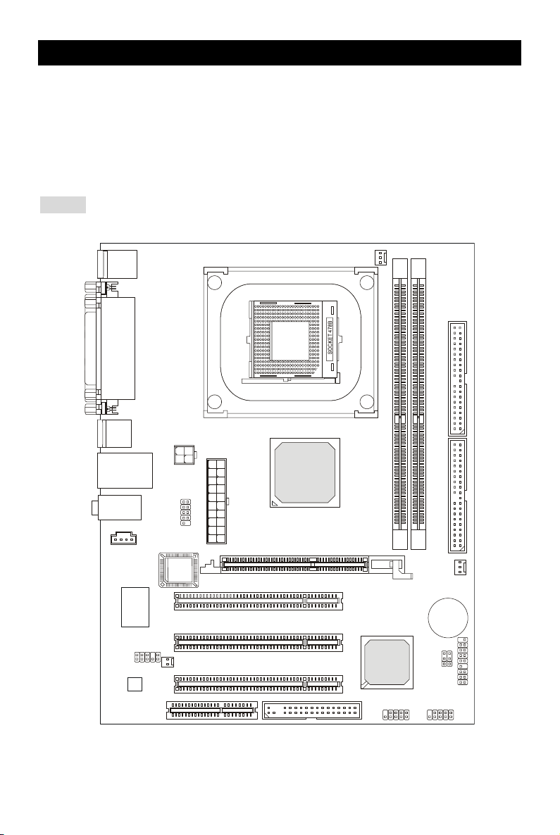
Layout
Top: M ou se
Bottom: Keyboard
Top: Parallel Port
Bottom:
COM
VGA Port
USB
Ports
Top: LAN Jack
Middle/Bottom:
USB Ports
T: Line-In
M:
Line-Out
B: Mic
CD_IN1
Port
F
d
H
n
7
o
9
b
6
n
3
i
8
W
W
JAUDIO1
Codec
JPW1
JCOM 2
S
O
I
B
JCASE1
ATX 1
CNR1
AGP Slot
PCI Slot 1
PCI Slot 2
PCI Slot 3
VIA
VT8751A
FDD 1
CFAN1
VT8237(R)
1
M
M
I
D
VIA
JUSB1 JUSB2
2
M
M
I
D
BATT
1
P
J
2
E
D
I
1
E
D
I
SFAN1
+
1
T
A
B
J
1
P
F
J
2
P
F
J
1
Page 6

Specifications
CPU
Supports Intel ® Pentium 4/Celeron (D) (Socket 478) processor up to 3.06GHz.
(For the latest information about CPU, please visit
http://www.msi.com.tw/program/products/mainboard/mbd/pro_mbd_cpu_support.php )
Chipset
VIA ® VT8751A (P4M266A) chipset (664 BGA)
- 64bit P4 processors FSB I/F (533MHz).
- 64bit DDR SDRAM memory I/F (200/266MHz).
- 32bit AGP I/F (66MHz) for 4x/2x mode.
- 8bit V-Link I/F (66MHz) with peak bandwidth of 266MB/s.
VIA ® VT8237(R) chipset (487 BGA)
- Integrated Hardware Sound Blaster/Direct Sound AC97 audio.
- Ultra DMA 66/100/133 master mode PCI EIDE controller.
- ACPI & PC2001 compliant enhanced power management.
- Supports USB2.0 up to 8 ports.
Main Memory
Supports four memory banks using two 184-pin DDR DIMM.
Supports up to 2GB PC2100/PC1600 DDR SDRAMs.
Supports 2.5v DDR SDRAM.
(For the updated supporting memory modules, please visit
http://www.msi.com.tw/program/products/mainboard/mbd/pro_mbd_trp_list.php )
Slots
One AGP (Accelerated Graphics Port) 4x slot (supports 1.5v only).
Three PCI 2.2 32-bit PCI bus slots (support 3.3v/5v PCI bus interface).
One CNR (Communication Network Riser) slot.
On-Board IDE
An IDE controller on the VIA ® VT8237(R) Chipset provides IDE HDD/CD-ROM with PIO,
Bus Master and Ultra DMA 33/66/100/133 operation modes. Can connect up to four IDE
devices.
2
Page 7

On-Board Peripherals
On-Board Peripherals include:
- 1 floppy port supports 2 FDDs with 360K, 720K, 1.2M, 1.44M and 2.88Mbytes.
- 1 serial port (COM 1).
- 1 parallel port supports SPP/EPP/ECP mode.
- 8 USB 2.0 ports (Rear * 4/ Front * 4).
- 1 audio (Line-In/Line-Out/Mic) port.
- 1 RJ45 LAN jack.
- 1 VGA port.
- 1 JCOM2 pin header.
- 2 IDE ports support 4 IDE devices.
Audio
AC97 link controller integrated in VT8237(R).
VIA ® VT1617A 6-channel software audio codec.
- Compliance with AC97 v2.3 spec.
LAN
VIA ® VT6103L 10/100 Mb/s phy.
- Supports 10Mb/s and 100Mb/s auto-negotiation operation.
- Compliance with PCI v2.2 and PC99 standard.
- Supports ACPI power management.
BIOS
The mainboard BIOS provides “Plug & Play” BIOS which detects the peripheral devices and
expansion cards of the board automatically.
The mainboard provides a Desktop Management Interface (DMI) function which records
your mainboard specifications.
Dimension
Micro-ATX Form Factor: 243 mm x 189mm.
Mounting
6 mounting holes.
3
Page 8
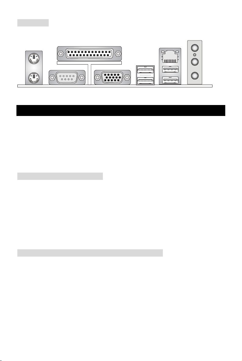
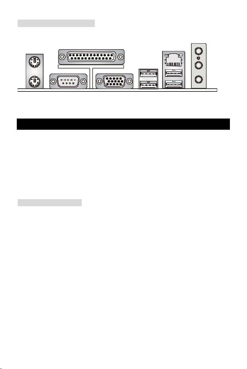
Rear Panel
V
The back panel provides the following connectors:
Mouse
Parallel Port
LAN
Line In
Keyboard
COM port
GA port
USB Ports
USB Ports
Line Out
Mic In
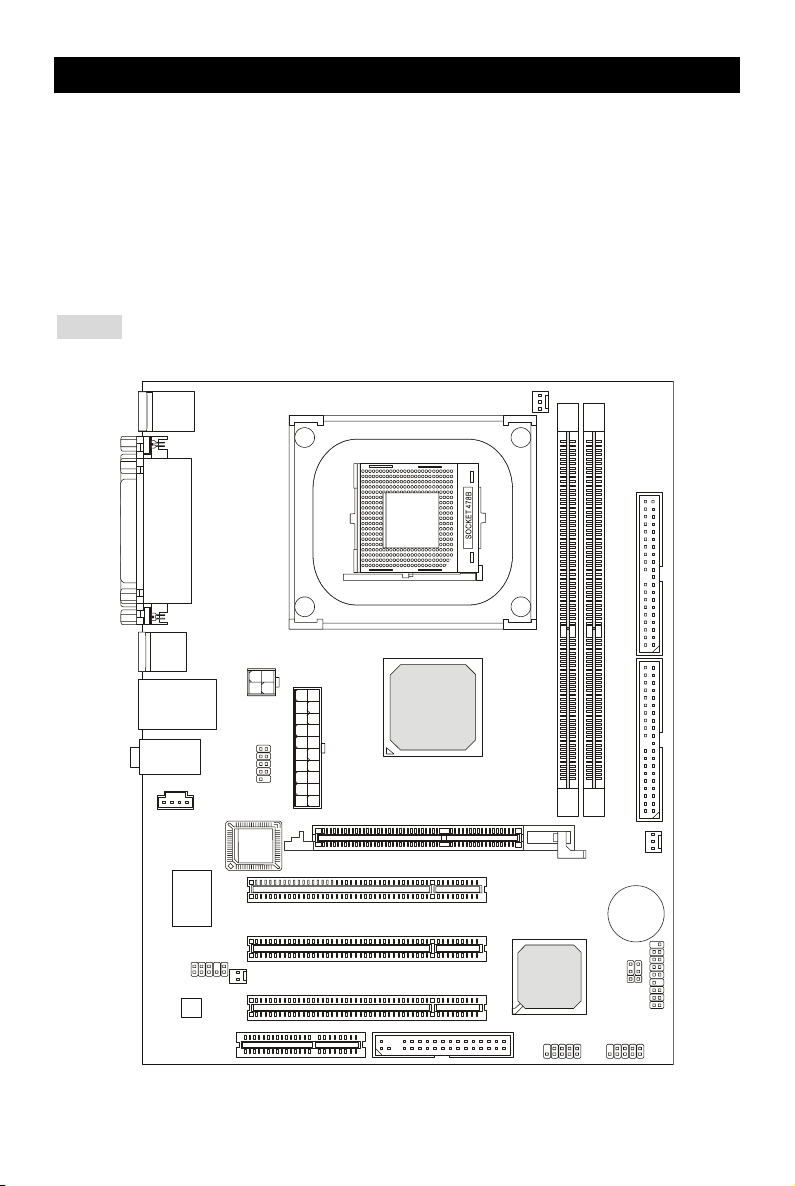
Hardware Setup
This chapter tells you how to install the CPU, memory modules, and expansion cards, as well as
how to setup the jumpers on the mainboard. It also provides the instructions on connecting the
peripheral devices, such as the mouse, keyboard, etc. While doing the installation, be careful in
holding the components and follow the installation procedures.
Central Processing Unit: CPU
The mainboard supports Intel Pentium 4/Celeron(D) processor in the 478 pin package. The
mainboard uses a CPU socket called PGA478 for easy CPU installation. When you are installing
the CPU, make sure the CPU has a heat sink and a cooling fan attached on the top to prevent
overheating. If you do not find the heat sink and cooling fan, contact your dealer to purchase and
install them before turning on the computer. (For the latest information about CPU, please visit
http://www.msi.com.tw/program/products/mainboard/mbd/pro_mbd_cpu_support.php )
Example of CPU Core Speed Derivation Procedure
If CPU Clock = 133MHz
Core/Bus ratio = 23
then CPU core speed = Host Clock x Core/Bus ratio
= 133MHz x 23
= 3.06 GHz
4
Page 9

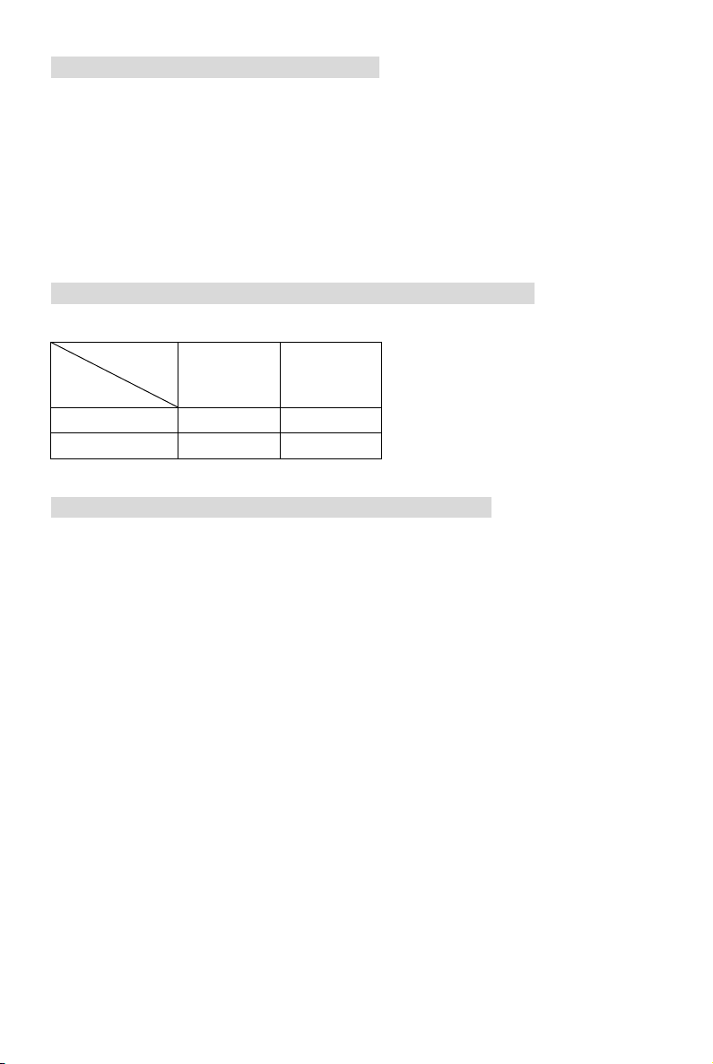
Memory Speed/CPU FSB Support Matrix
Memory
FSB
400 MHz OK OK
533 MHz OK OK
DDR 200 DDR 266
CPU Installation Procedures for Socket 478
1. Please turn off the power and unplug the power cord before installing the CPU.
2. Pull the lever sideways away from the socket. Make sure to raise the lever up to a
90-degree angle.
3. Look for the gold arrow. The gold arrow should point towards the lever pivot. The CPU can
only fit in the correct orientation.
4. If the CPU is correctly installed, the pins should be completely embedded into the socket
and can not be seen. Please note that any violation of the correct installation procedures
may cause permanent damages to your mainboard.
5. Press the CPU down firmly into the socket and close the lever. As the CPU is likely to
move while the lever is being closed, always close the lever with your fingers pressing
tightly on top of the CPU to make sure the CPU is properly and completely embedded into
the socket.
Installing the CPU Fan
As processor technology pushes to faster speeds and higher performance, thermal management
becomes increasingly important. To dissipate heat, you need to attach the CPU cooling fan and
heatsink on top of the CPU. Follow the instructions below to install the Heatsink/Fan:
1. Locate the CPU and its retention mechanism on the motherboard.
2. Position the heatsink onto the retention mechanism.
3. Mount the fan on top of the heatsink. Press down the fan until its four clips get wedged in
the holes of the retention mechanism.
4. Press the two levers down to fasten the fan. Each lever can be pressed down in only ONE
5
Page 10

direction.
5. Connect the fan power cable from the mounted fan to the 3-pin fan power connector on
the board.
MSI Reminds You...
Overheating…
Overheating will seriously damage the CPU and system, always make sure the cooling fan can
work properly to protect the CPU from overheating.
Replacing the CPU…
While replacing the CPU, always turn off the ATX power supply or unplug the power supply’s
power cord from grounded outlet first to ensure the safety of CPU.
Memory
The mainboard provides two 184-pin unbuffered DDR200/DDR266 DDR SDRAM, and supports
the memory size up to 2GB. To operate properly, at least one DIMM module must be installed.
(For the updated supporting memory modules, please visit
http://www.msi.com.tw/program/products/mainboard/mbd/pro_mbd_trp_list.php )
Install at least one DIMM module on the slots. Memory modules can be installed on the slots in
any order. You can install either single- or double-sided modules to meet your own needs.
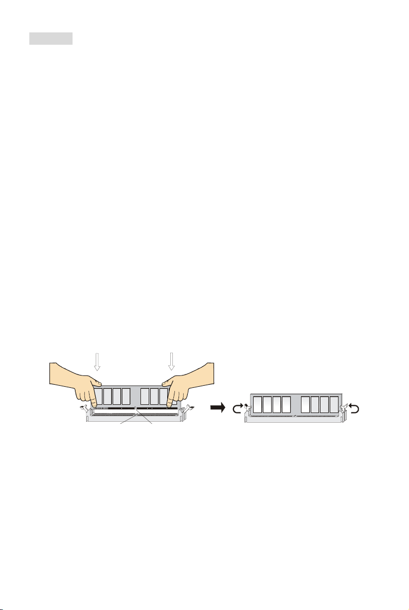
Installing DDR Modules
1. The DDR DIMM has only one notch on the center of module. The module will only fit in the
right orientation.
2. Insert the DIMM memory module vertically into the DIMM slot. Then push it in until the
golden finger on the memory module is deeply inserted in the socket.
3. The plastic clip at each side of the DIMM slot will automatically close.
6
Page 11
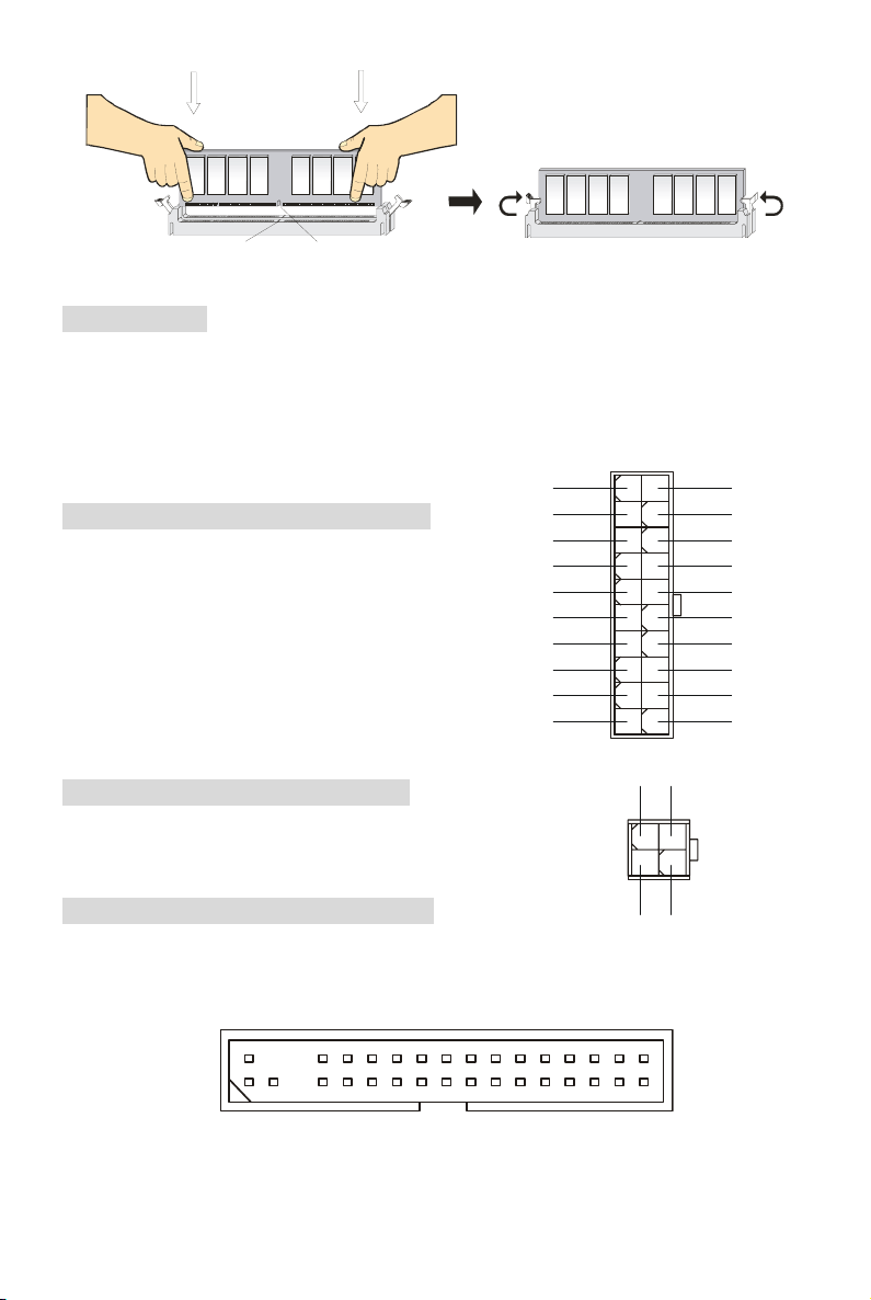
NotchVol t
4
G
Power Supply
The mainboard supports ATX power supply for the power system. Before inserting the power
supply connector, always make sure that all components are installed properly to ensure that no
damage will be caused. A 300W or above power supply is suggested.
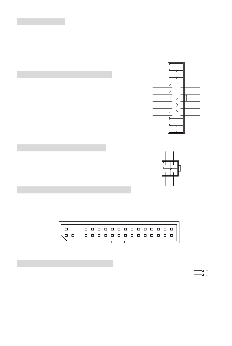
ATX 20-Pin Power Connector: ATX1
This connector allows you to connect to an ATX power
supply. To connect to the ATX power supply, make sure
the plug of the power supply is inserted in the proper
orientation and the pins are aligned. Then push down
the power supply firmly into the connector.
12V
5V_SB
PW_OK
GND
5V
GND
5V
GND
3.3V
3.3V
10 20
111
GND
5V
5V
-5V
GND
GND
GND
PS_ON
GND
-12V
3.3V
12V
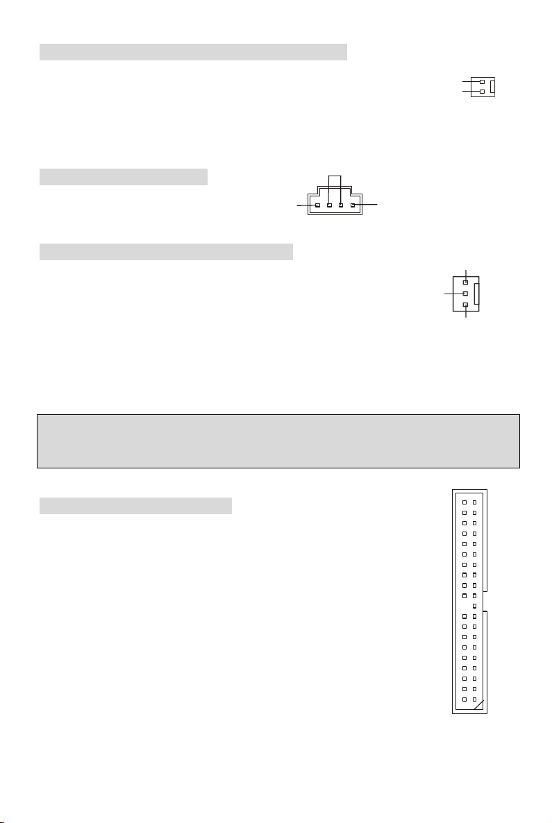
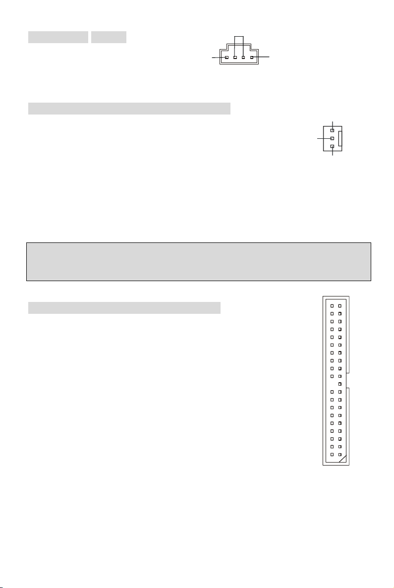
ATX 12V Power Connector: JPW1
This 12V power connector is used to provide power to the CPU.
1
2
3
Floppy Disk Drive Connector: FDD1
12V
ND
The mainboard provides a standard floppy disk drive connector that supports 360K, 720K, 1.2M,
1.44M and 2.88M floppy disk types.
7
Page 12
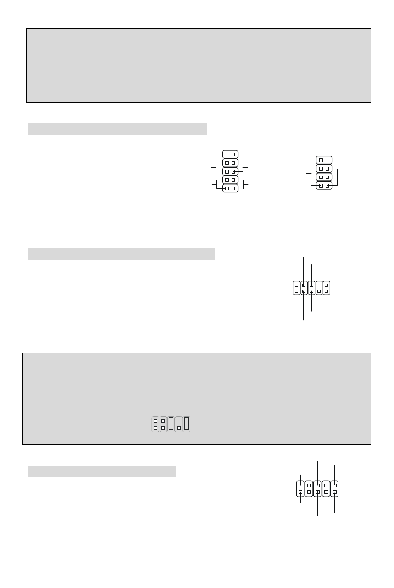
Chassis Intrusion Switch Connector: JCASE1
SENSO
This connector is connected to 2-pin connector chassis switch. If the Chassis is
open, the switch will be short. The system will record this status. To clear the
warning, you must enter the BIOS setting and clear the status.
CD-In Connector: CD_IN1
GND
The connector is for CD-ROM audio connector.
R
L
Fan Power Connectors: CFAN1/SFAN1
The CFAN1 (processor fan) and SFAN1 (system fan) support system cooling
fan with +12V. They support three-pin head connector. When connecting the
wire to the connectors, always take note that the red wire is the positive and
should be connected to the +12V, the black wire is Ground and should be
connected to GND.
MSI Reminds You...
Always consult the vendors for proper CPU cooling fan.
+12V
GND
CINTRU
R
GND
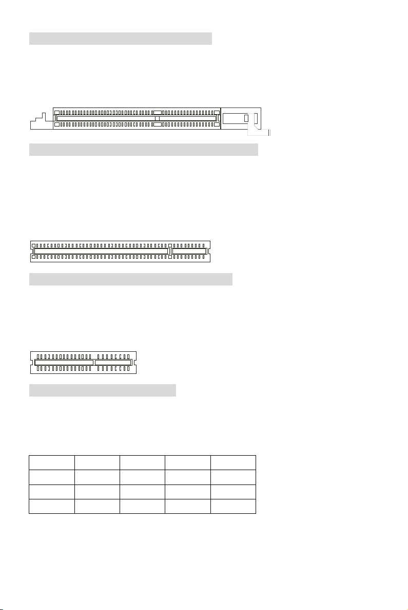
IDE Connectors: IDE1 & IDE2
The mainboard has a 32-bit Enhanced PCI IDE and Ultra DMA 33/66/100/133
controller that provides PIO mode 0~4, Bus Master, and Ultra DMA 33/66/100/133
function. You can connect up to four hard disk drives, CD-ROM, 120MB Floppy
and other devices.
The first hard drive should always be connected to IDE1. IDE1 can connect a
Master and a Slave drive. You must configure second hard drive to Slave mode by
setting the jumper accordingly. IDE2 can also connect a Master and a Slave drive.
8
Page 13
MSI Reminds You...
r
9
2
_
A
S
If you install two hard disks on cable, you must configure the second drive to Slave mode by
setting its jumper. Refer to the hard disk documentation supplied by hard disk vendors for jumper
setting instructions.
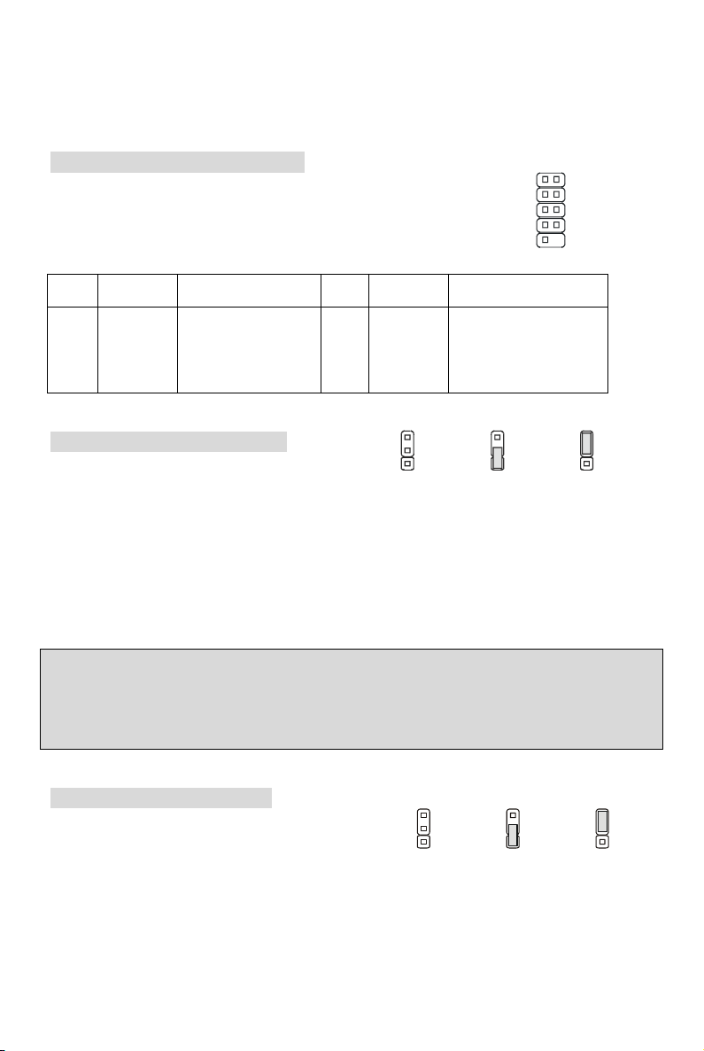
Front Panel Connectors: JFP1 & JFP2
Power
Switch
Power
LED
10
78
Reset
Switch
HDD
LED
1
Speaker
Powe
LED
12
The mainboard provides two front panel
connectors for electrical connection to the
front panel switches and LEDs. JFP1 is
compliant with Intel Front Panel I/O
Connectivity Design Guide. JFP1 JFP2
Front Panel Audio Connector: JAUDIO1
The front panel audio connector allows you to connect to the front
panel audio and is compliant with Intel ® Front Panel I/O
Connectivity Design Guide.
UD_GND
2
1
AUD_MIC
AUD_VCC
AUD
MIC_BIAS
AUD_RET_R
KEY
AUD_RET_L
AUD_FPOUT_L
NC
AUD_FPOUT_R
10
9
MSI Reminds You...
If you do not want to connect to the front audio header, pins 5 & 6, 9 & 10 have to be jumpered in
order to have signal output directed to the rear audio ports. Otherwise, the Line-Out connector on
2
the back panel will not function.
1
Front USB Connector: JUSB1/2
The mainboard provides two standard USB 2.0 pin header JUSB1 &
JUSB2. USB 2.0 technology increases data transfer rate up to a
maximum throughput of 480Mbps, which is 40 times faster than USB
10
9
9
KEY
9
10
NC
GND
GND
USB0+
USB1+
U
USB1-
B0-
VCC
1
2
VCC
Page 14
1.1, and is ideal for connecting high-speed USB interface peripherals such as USB HDD, digital
a
U
cameras, MP3 players, printers, modems and the like.
Serial Port Connector: JCOM2
1
The mainboard offers another serial port JCOM2. It is 16550A high speed
communication port that sends/receives 16 bytes FIFOs. The MSI JCOM2
cable is optional.
9210
PIN SIGNAL DESCRIPTION PIN SIGNAL DESCRIPTION
1
3
5
7
9
DCD
SOUT
GND
RTS
RI
Data Carry Detect
Receive Data Transmit
Data
Request To Send Ring
Indicate
2
4
6
8
10
SIN
DTR
DSR
CTS
X
Serial in or receive data
Serial out or transmit data
Data Set Ready
Clear To Send
X
Clear CMOS Jumper: JBAT1
There is a CMOS RAM on board that has a power
3
1
1
Keep Data
(Default)
3
1
Clear Dat
supply from external battery to keep the system
configuration data. With the CMOS RAM, the system can automatically boot OS every time it is
turned on. If you want to clear the system configuration data, use the JBAT1 (Clear CMOS
Jumper) to clear data. Follow the instructions below to clear the data:
MSI Reminds You...
You can clear CMOS by shorting 2-3 pin while the system is off. Then return to 1-2 pin position.
Avoid clearing the CMOS while the system is on; it will damage the mainboard.
CPU Support Jumper: JP1
This jumper specifies the mainboard’s support for
locked or some unlocked CPU.
3
1
1
Locked CPU
(De fau lt)
3
1
Unlocked CP
10
Page 15
AGP (Accelerated Graphics Port) Slot
The AGP slot allows you to insert the AGP graphics card. AGP is an interface specification
designed for the throughput demands of 3D graphics. It introduces a 66MHz, 32-bit channel for
the graphics controller to directly access main memory. The mainboard supports 4x AGP card.
PCI (Peripheral Component Interconnect) Slots
The PCI slots allow you to insert the expansion cards to meet your needs. When adding or
removing expansion cards, make sure that you unplug the power supply first. Meanwhile, read
the documentation for the expansion card to make any necessary hardware or software settings
for the expansion card, such as jumpers, switches or BIOS configuration.
CNR (Communication Network Riser) Slot
The CNR slot allows you to insert the CNR expansion cards. CNR is a specially designed
network, audio, or modem riser card for ATX family motherboards. Its main processing is done
through software and controlled by the motherboard chipset.
PCI Interrupt Request Routing
The IRQ, abbreviation of interrupt request line and pronounced I-R-Q, are hardware lines over
which devices can send interrupt signals to the microprocessor. The PCI IRQ pins are typically
connected to the PCI bus INT A# ~ INT D# pins as follows:
Order1 Order2 Order3 Order4
PCI Slot 1 INT A# INT B# INT C# INT D#
PCI Slot 2 INT B# INT C# INT D# INT A#
PCI Slot 3 INT C# INT D# INT A# INT B#
11
Page 16
BIOS Setup
Power on the computer and the system will start POST (Power On Self Test) process. When the
message below appears on the screen, press <DEL> key to enter Setup.
If the message disappears before you respond and you still wish to enter Setup, restart the
system by turning it OFF and On or pressing the RESET button. You may also restart the system
by simultaneously pressing <Ctrl>, <Alt>, and <Delete> keys.
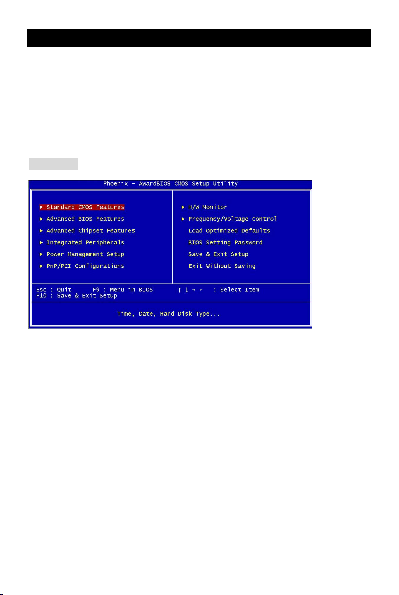
Main Page
Standard CMOS Features
Use this menu for basic system configurations, such as time, date etc.
Advanced BIOS Features
Use this menu to setup the items of Award special enhanced features.
Advanced Chipset Features
Use this menu to change the values in the chipset registers and optimize your system
performance.
Integrated Peripherals
Use this menu to specify your settings for integrated peripherals.
Power Management Setup
Use this menu to specify your settings for power management.
PNP/PCI Configurations
This entry appears if your system supports PnP/PCI.
H/W Monitor
This entry shows the status of your CPU, fan, warning for overall system status.
Frequency/Voltage Control
Use this menu to specify your settings for frequency/voltage control.
12
Page 17

Load Optimized Defaults
Use this menu to load the default values set by the mainboard manufacturer specifically for
optimal performance of the mainboard.
BIOS Setting Password
Use this menu to set BIOS setting Password.
Save & Exit Setup
Save changes to CMOS and exit setup.
Exit Without Saving
Abandon all changes and exit setup.
13
Page 18
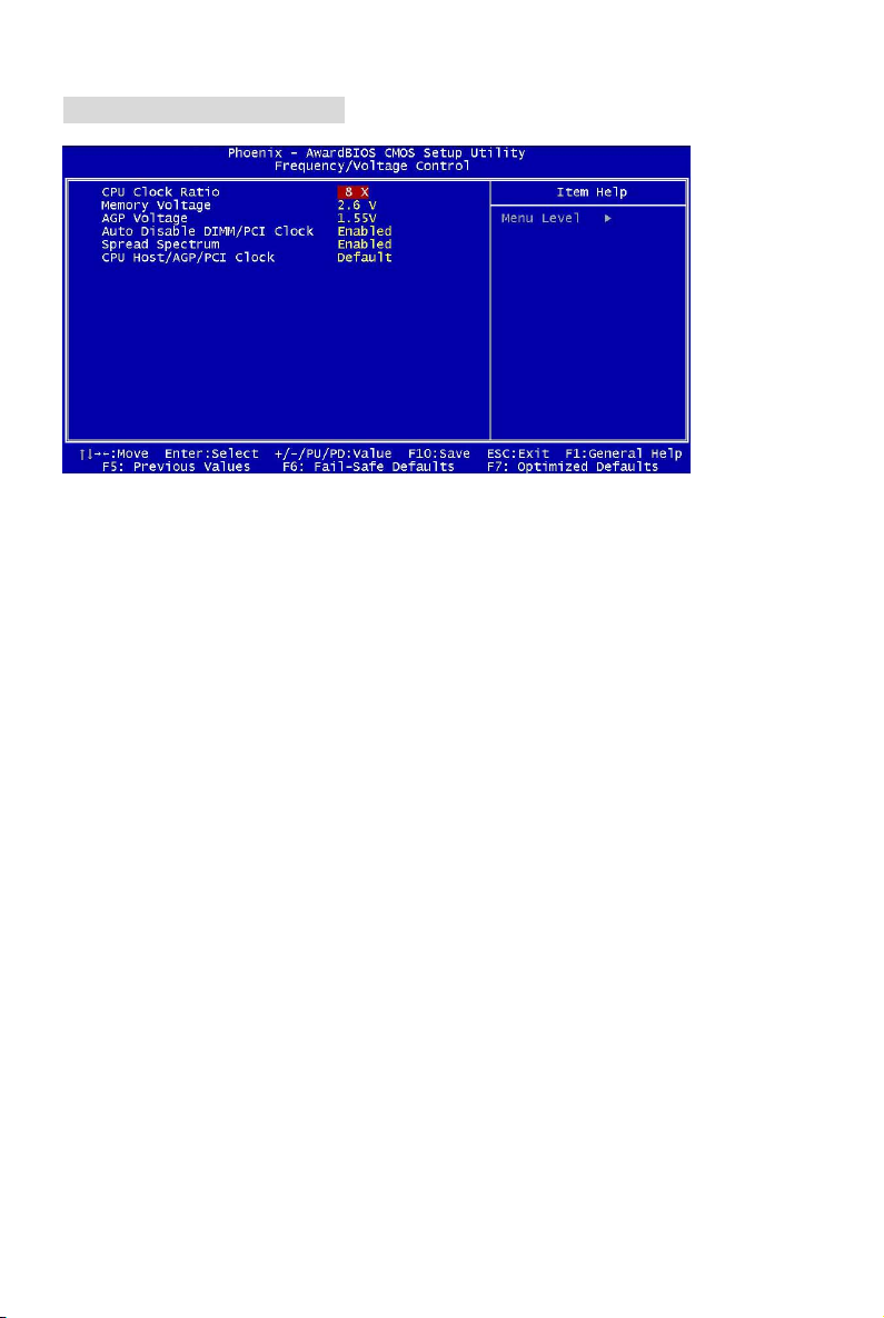
Frequency/Voltage Control
CPU Clock Ratio
End users can overclock the processor (only if the processor supports so) by specifying the CPU
ratio (clock multiplier) in this field.
Memory Voltage
Adjusting the DDR voltage can increase the DDR speed. Any changes made to this setting
may cause a stability issue, so changing the DDR voltage for long-term purpose is NOT
recommended.
AGP Voltage
AGP voltage is adjustable in the field, allowing you to increase the performance of your AGP
display card when overclocking, but the stability may be affected. Setting options: 1.5V to 1.8V at
0.05V increment.
Auto Disable DIMM/PCI Clock
This item is used to auto detect the PCI slots. When set to Enabled, the system will remove (turn
off) clocks from empty PCI slots to minimize the electromagnetic interference (EMI).
Spread Spectrum
When the motherboard’s clock generator pulses, the extreme values (spikes) of the pulses
creates EMI (Electromagnetic Interference). The Spread Spectrum function reduces the EMI
generated by modulating the pulses so that the spikes of the pulses are reduced to flatter curves.
If you do not have any EMI problem, leave the setting at Disabled for optimal system stability and
performance. But if you are plagued by EMI, set to Enabled for EMI reduction. Remember to
disable Spread Spectrum if you are overclocking because even a slight jitter can introduce a
temporary boost in clock speed which may just cause your overclocked processor to lock up.
CPU Host/AGP/PCI Clock
Use this item to select the appropriate clock frequency of the CPU host/AGP/PCI bus.
14
Page 19
Einleitung
Danke, dass Sie das P4MAM2-V Series (MS-7095 v1.X) Mikro ATX Mainboard erworben haben.
Das P4MAM2-V Series basiert auf den VIA ® VT8751A (P4M266A) und VT8237(R) Chipsätzen
und ermöglicht so ein optimales und effizientes System. Entworfen um die fortschrittlichen Intel
® Pentium ® 4 /Celeron(D) Prozessoren mit 478 Pins aufzunehmen, stellt das P4MAM2-V
Series die ideale Lösung zum Aufbau eines professionellen Hochleistungsdesktopsystems dar.
Layout
Top: M ou se
Bottom: Keyboard
Top: Parallel Port
Bottom:
COM
Port
VGA Port
USB
Ports
Top: LAN Jack
Middle/Bottom:
USB Ports
T: Line-In
M:
Line-Out
B: Mic
CD_IN1
F
d
H
n
7
o
9
b
6
n
3
i
8
W
W
JAUDIO1
Codec
JPW1
JCOM 2
S
O
I
B
JCASE1
ATX 1
CNR1
AGP Slot
PCI Slot 1
PCI Slot 2
PCI Slot 3
VIA
VT8751A
FDD 1
CFAN1
VT8237(R)
1
M
M
I
D
VIA
JUSB1 JUSB2
2
M
M
I
D
BATT
1
P
J
2
E
D
I
1
E
D
I
SFAN1
+
1
T
A
B
J
1
P
F
J
2
P
F
J
15
Page 20

Spezifikationen
CPU
Unterstützt Intel ® Pentium 4/Celeron (D) (Sockel 478) Prozessoren mit bis zu 3.06GHz.
(Um die neuesten Informationen zu unterstützten Prozessoren zu erhalten, besuchen Sie bitte
http://www.msi.com.tw/program/products/mainboard/mbd/pro_mbd_cpu_support.php )
Chipsatz
VIA ® VT8751A (P4M266A) Chipsatz (664 BGA)
- 64 Bit P4 Prozessoren FSB Schnittstelle (533MHz).
- 64 Bit DDR SDRAM Schnittstelle (200/266MHz).
- 32 Bit AGP Schnittstelle (66MHz) in den Modi 4x/2x.
- 8 Bbit V-Link Schnittstelle (66MHz) mit Spitzenbandbreite von 266MB/s.
VIA ® VT8237(R) Chipsatz (487 BGA)
- Integrierte Hardware Sound Blaster/ Direct Sound AC97 Audiolösung.
- Ultra DMA 66/100/133 PCI EIDE Kontroller, der Betrieb im Master Modus unterstützt
- erweiterte Stromsparfunktionalität gemäß ACPI und PC2001
- Unterstützt USB2.0 mit bis zu 8 Anschlüssen.
Hauptspeicher
Unterstützt vier Speicherbänke für zwei 184-pin DDR DIMMs.
Unterstützt den Speicherausbau auf bis zu 2GB PC2100/PC1600 DDR SDRAMs.
Unterstützt 2.5V DDR SDRAMs.
(Um den letzten Stand bezüglich der unterstützten Speichermodule zu erhalten, besuchen Sie
bitte http://www.msi.com.tw/program/products/mainboard/mbd/pro_mbd_trp_list.php )
Schnittstellen
Eine AGP (Accelerated Graphics Port) 4x Schnittstelle (unterstützt nur 1.5V).
Drei PCI 2.2 32-Bit PCI Bus Sockel (3.3V/5V PCI Bus unterstützt).
Ein CNR (Communication Network Riser) Sockel.
On-Board IDE
Der im VIA ® VT8237(R) Chipsatz enthaltene IDE Kontroller bietet für den Festplatten- und
CD-ROM-Zugriff PIO, Bus Mastering und Betrieb mit Ultra DMA 33/66/100/133. Bis zu vier
IDE Geräte anschließbar.
16
Page 21

Peripherieanschlüsse onboard
hierzu gehören:
- 1 Anschluss für zwei Diskettenlaufwerke mit 360 KB, 720 KB, 1,2 MB, 1,44 MB oder
2,88 MB.
- 1 Serielle Schnittstelle (COM 1).
- 1 Parallele Schnittstelle, die die Betriebsmodi SPP/EPP/ECP unterstützt.
- 8 USB 2.0 Anschlüsse (4 hintere/ 4 vordere).
- 1 Satz Audioanschlüsse (Eingang/ Ausgang/ Mikrofon).
- 1 RJ45 LAN Buchse.
- 1 VGA Anschluss.
- 1 serielle Schnittstelle JCOM2, ausgeführt als Stiftleiste.
- 2 IDE Anschlüsse, die bis zu 4 IDE Geräte unterstützen.
Audio
In den VT8237(R) integrierter AC97 Anschlusskontroller.
VIA ® VT1617A 6-Kanal Software Audio Codec.
- Erfüllt die Anforderungen der Spezifikation AC97 V2.3.
LAN
VIA ® VT6103L 10/100 MB/s PHY.
- Unterstützt Betrieb mit 10Mb/s oder 100Mb/s, automatisch gewählt.
- Entspricht den Standards PCI V2.2 und PC99.
- Unterstützt ACPI Stromsparfunktionalität.
BIOS
Das Mainboard-BIOS verfügt über “Plug & Play”-Funktionalität, mit der angeschlossene
Peripheriegeräte und Erweiterungskarten automatisch erkannt werden.
Das Mainboard stellt ein Desktop - Management - Interface (DMI) zur Verfügung, welches
automatisch die Spezifikationen Ihres Mainboards aufzeichnet.
Abmessungen
Mikro- ATX Form Faktor: 243 mm x 189mm.
Montage
6 Montagebohrungen.
17
Page 22
Hinteres Anschlusspaneel
Das hintere Panel verfügt über folgende Anschlüsse:
Maus
Parallel Port
LAN
Line In
Tast atu r
Serieller Anschl uss
VGA Anschl uss
USB Ports
USB Ports
Line Out
Mic In
Hardware Setup
Dieses Kapitel informiert Sie darüber, wie Sie die CPU, Speichermodule und Erweiterungskarten
einbauen, des weiteren darüber, wie die Steckbrücken auf dem Mainboard gesetzt werden.
Zudem bietet es Hinweise darauf, wie Sie Peripheriegeräte anschließen, wie z.B. Maus, Tastatur,
usw. Handhaben Sie die Komponenten während des Einbaus vorsichtig und halten Sie sich an
die vorgegebene Vorgehensweise beim Einbau.
Hauptprozessor: CPU
Das Mainboard unterstützt Intel Pentium 4 / Celeron(D) Prozessoren mit 478 Pins. Hierbei setzt
das Mainboard den CPU Sockel PGA478 ein, um den CPU- Einbau zu erleichtern. Achten Sie
beim Einbau bitte darauf, dass die CPU immer mit einem Kühlkörper mit aktivem Prozessorlüfter
versehen sein muss, um Überhitzung zu vermeiden. Verfügen Sie über keinen Kühlkörper mit
aktivem Prozessorlüfter, setzen Sie sich bitte mit Ihrem Händler in Verbindung, um einen solchen
zu erwerben und danach zu installieren, bevor Sie Ihren Computer anschalten.
(Um die neuesten Informationen zu unterstützten Prozessoren zu erhalten, besuchen Sie bitte
http://www.msi.com.tw/program/products/mainboard/mbd/pro_mbd_cpu_support.php)
18
Page 23
Beispiel zur Ermittlung des Kerntaktes
Wenn externer CPU-Takt = 133 MHz
Kern-/Systemtaktmultiplikator = 23
dann ist Kerntakt = externer CPU-Takt x Kern/Sytemtaktmultiplikator
= 133 MHz x 23
= 3,06 GHz
Tabelle Speichergeschwindigkeit/ unterstützter CPU FSB
Speicher
FSB
400 MHz OK OK
533 MHz OK OK
DDR 200 DDR 266
Vorgehensweise beim CPU-Einbau beim Sockel 478
1. Bitte schalten Sie das System aus und ziehen Sie den Netzstecker, bevor Sie die CPU
einbauen.
2. Ziehen Sie den Hebel leicht seitlich weg vom Sockel, heben Sie ihn danach bis zu einem
Winkel von 90° an.
3. Machen Sie den goldenen Pfeil ausfindig, er sollte auf das Hebelgelenk zeigen. Die CPU
passt nur in der korrekten Ausrichtung.
4. Ist die CPU korrekt installiert, sollten die Pins an der Unterseite vollständig versenkt und
nicht mehr sichtbar sein. Beachten Sie bitte, dass jede Abweichung von der richtigen
Vorgehensweise beim Einbau Ihr Mainboard dauerhaft beschädigen kann.
5. Drücken Sie die CPU fest in den Sockel und drücken Sie den Hebel wieder nach unten bis
in seine Ursprungsstellung. Da die CPU während des Schließens des Hebels dazu neigt,
sich zu bewegen, sichern Sie diese bitte während des Vorgangs durch permanenten
Fingerdruck von oben, um sicherzustellen, dass die CPU richtig und vollständig im Sockel
sitzt.
19
Page 24

Installation des CPU Kühlers
Mit dem Fortschritt der Prozessortechnologie, der zu immer höheren Geschwindigkeiten und
Leistungen führt, wird Temperaturkontrolle immer wichtiger. Um die Hitze abzuleiten, müssen Sie
einen CPU-Kühler mit Lüfter auf der CPU installieren. Befolgen Sie zur Installation des Kühlers
die folgenden Anweisungen:
1. Machen Sie die CPU und ihren Rückhaltemechanismus auf dem Motherboard ausfindig.
2. Platzieren Sie den Kühlkörper auf dem Rückhaltemechanismus.
3. Setzen Sie den Lüfter auf den Kühlkörper. Pressen Sie den Lüfter nach unten, bis seine
vier Klammern in den Löchern des Rückhaltemechanismus einrasten. Drücken Sie die
zwei Hebel herab, um den Lüfter zu befestigen. Jeder Hebel kann nur in EINER Richtung
herabgedrückt werden.
4. Verbinden Sie das Stromkabel des montierten Lüfters mit dem 3-poligen
Stromanschluss auf dem Board.
MSI weist darauf hin...
Überhitzung …
Überhitzung beschädigt die CPU und das System nachhaltig, stellen Sie stets eine korrekte
Funktionsweise des CPU Kühlers sicher, um die CPU vor Überhitzung zu schützen.
Auswechseln der CPU …
Stellen Sie während eines CPU-Wechsels immer sicher, dass das ATX Netzteil ausgeschaltet ist
und ziehen Sie zuerst den Netzstecker, um die Unversehrtheit Ihrer CPU zu gewährleisten.
20
Page 25
Speicher
Das Mainboard bietet Platz für zwei ungepufferte 184-Pin DDR200/DDR266 DDR SDRAMs und
unterstützt den Speicherausbau auf bis zu 2GB. Um einen ordnungsgemäßen Betrieb zu
ermöglichen, muss mindestens ein DIMM- Speichermodul eingesetzt sein.
(Um den letzten Stand bezüglich der unterstützten Speichermodule zu erhalten, besuchen Sie
bitte http://www.msi.com.tw/program/products/mainboard/mbd/pro_mbd_trp_list.php)
Setzen Sie mindestens ein Speichermodul in einen Stecksockel. Die Speichermodule können in
beliebiger Reihenfolge eingesetzt werden. Gemäß Ihren Anforderungen können Sie entweder
ein- oder doppelseitige Module verwenden .
Vorgehensweise beim Einbau von DDR Modulen
1. DDR DIMMs haben nur eine Kerbe in der Mitte des Moduls. Sie passen nur in einer
Richtung in den Sockel.
2. Setzen Sie den DIMM- Speicherbaustein senkrecht in den DIMM- Sockel, dann drücken
Sie ihn hinein, bis die goldenen Kontakte tief im Sockel sitzen.
3. Die Plastikklammern an den Seiten des DIMM- Sockels schließen sich automatisch.
Vol t
Kerbe
21
Page 26
Stromversorgung
4
G
Das Mainboard unterstützt zur Stromversorgung ATX Netzteile. Bevor Sie den Netzteilstecker
einstecken, stellen Sie stets sicher, dass alle Komponenten ordnungsgemäß eingebaut sind, um
Schäden auszuschließen. Es wird ein Netzteil mit 300W oder mehr empfohlen.
ATX 20-Pin Stromanschluss: ATX1
Hier können Sie ein ATX Netzteil anschließen. Wenn Sie
die Verbindung herstellen, stellen Sie sicher, dass der
Stecker in der korrekten Ausrichtung eingesteckt wird und
die Pins ausgerichtet sind. Drücken Sie dann den
Netzteilstecker fest in den Steckersockel.
12V
5V_SB
PW_OK
GND
5V
GND
5V
GND
3.3V
3.3V
10 20
5V
5V
-5V
GND
GND
GND
PS_ON
GND
-12V
3.3V
111
ATX 12V Stromanschluss: JPW1
GND
12V
Dieser 12V Stromanschluss wird verwendet, um die CPU mit Strom
zu versorgen.
1
2
3
12V
Anschluss des Diskettenlaufwerks: FDD1
ND
Das Mainboard verfügt über einen Standardanschluss für ein Diskettenlaufwerk mit 360 KB, 720
KB, 1,2 MB, 1,44 MB oder 2,88 MB Kapazität.
Gehäusekontaktschalter: JCASE1
GND
Dieser Anschluss ist mit einem zweipoligen Schalter am Gehäuse verbunden.
Wird das Gehäuse geöffnet, wird der Kontakt des Schalters geschlossen. Das System zeichnet
dies. Um die resultierende Warnung zu löschen, müssen Sie das BIOS aufrufen und die
Aufzeichnung löschen.
CINTRU
22
Page 27
CD-Eingang: CD_IN1
SENSO
GND
Hier kann das Audiokabel des CD-ROM
R
L
Laufwerkes angeschlossen werden.
Stromanschlüsse für Lüfter: CFAN1/SFAN1
Die Anschlüsse CFAN1 (Prozessorlüfter) und SFAN1 (Systemlüfter)
unterstützen aktive Systemlüfter mit + 12V und einem 3-Poligen Stecker.
+12V
Wenn Sie den Stecker mit dem Anschluss verbinden, sollten Sie immer
darauf achten, dass der rote Draht der positive Pol ist, und mit +12V
verbunden werden sollte, der schwarze Draht ist der Erdkontakt und sollte mit GND verbunden
werden.
R
GND
MSI weist darauf hin...
Bitten Sie stets Ihren Händler um Hilfe bei der Auswahl des geeigneten CPU Kühlers.
Anschlüsse der Festplatten: IDE1 & IDE2
Das Mainboard besitzt einen 32-Bit Enhanced PCI IDE und Ultra DMA
33/66/100/133 Kontroller, der die PIO Modi 0- 4 bereitstellt, Bus Mastering
beherrscht und Ultra DMA 33/66/100/133 Funktionalität bietet. Es können bis zu
vier Festplatten, CD-ROM-, 120MB Disketten-Laufwerke und andere Geräte
angeschlossen werden.
Die erste Festplatte sollte immer an IDE1 angeschlossen werden. IDE1 kann ein
Master- und ein Slave- Laufwerk verwalten. Die zweite Festplatte muss durch das
entsprechende Setzen einer Steckbrücke als Slave eingestellt werden. IDE2 kann
ebenfalls je ein Master- und ein Slave- Laufwerk verwalten.
23
Page 28

MSI weist darauf hin...
_
A
r
9
2
Verbinden Sie zwei Laufwerke über ein Kabel, müssen Sie das zweite Laufwerk im Slave-Modus
konfigurieren, indem Sie entsprechend den Jumper setzen. Entnehmen Sie bitte die Anweisun-
gen zum Setzen des Jumpers der Dokumentation der Festplatte, die der Festplattenhersteller
zur Verfügung stellen.
Frontpanel Anschlüsse: JFP1 & JFP2
Das Mainboard verfügt über zwei Anschlüsse für
das Frontpanel, diese dienen zum Anschluss
der Schalter und LEDs des Frontpanels. JFP1
erfüllt die Anforderungen des “Intel Front Panel
Power
Switch
Power
LED
10
Reset
Switch
HDD
LED
Speaker
1
78
12
I/O Connectivity Design Guide“. JFP1 JFP2
Front Panel Audio Anschluss: JAUDIO1
Der Audio Vorderanschluss ermöglicht den Anschluss von Audioein-
und -ausgängen eines Frontpanels. Der Anschluss entspricht den
Richtlinien des “Intel® Front Panel I/O Connectivity Design Guide”.
UD_GND
2
1
AUD_MIC
AUD_VCC
AUD
MIC_BIAS
AUD_RET_R
KEY
AUD_RET_L
AUD_FPOUT_L
NC
AUD_FPOUT_R
10
9
MSI weist darauf hin...
Wenn Sie die vorderen Audioanschlüsse nicht verwenden, müssen die Pins 5 & 6, 9 & 10 mit
sog. „Jumpern“ gebrückt werden, um die Signalausgabe auf die hinteren Audioanschlüsse
umzuleiten. Andernfalls ist der Line -Out Ausgang im hinteren Anschlussfeld ohne Funktion.
Powe
LED
2
1
10
9
24
Page 29

USB Vorderanschluss: JUSB1/2
S
Das Mainboard verfügt über zwei Standard- USB- 2.0- Anschlüsse in Form
der Stift- Blöcke JUSB1 und JUSB2. Die USB 2.0 Technologie erhöht den
Datendurchsatz auf maximal 480Mbps, 40 mal schneller als USB 1.1 und ist
bestens geeignet, Hochgeschwindigkeits- USB- Peripheriegeräte
anzuschließen, wie z.B. USB Festplattenlaufwerke, Digitalkameras,
MP3-Player, Drucker, Modems und ähnliches.
10
U
B0-
USB0+
VCC
GND
KEY
9
NC
GND
USB1+
1
2
VCC
USB1-
Serieller Anschluss: JCOM2
1
Das Mainboard bietet einen zusätzlichen Seriellen Anschluss JCOM2.
Es handelt sich um eine 16550A Hochgeschwindigkeitskommunikations-
schnittstelle, die 16 Bytes FIFOs sendet/empfängt. Das MSI JCOM2
9210
Kabel ist optional.
PIN SIGNAL BESCHREIBUNG PIN SIGNAL BESCHREIBUNG
1
3
5
7
9
DCD
SOUT
GND
RTS
RI
Data Carry Detect
Receive Data Transmit
Data
Request To Send Ring
Indicate
2
4
6
8
10
SIN
DTR
DSR
CTS
X
Serial in or receive data
Serial out or transmit data
Data Set Ready
Clear To Send
X
25
Page 30

Steckbrücke zur CMOS-Löschung: JBAT1
a
U
Auf dem Mainboard gibt es einen sogenannten
CMOS Speicher (RAM), der über eine Batterie
gespeist wird und die Daten der
3
1
1
Keep Data
(Default)
3
1
Clear Dat
Systemkonfiguration enthält. Er ermöglicht es dem
Betriebssystem, mit jedem Einschalten automatisch hochzufahren. Wollen Sie die
Systemkonfiguration löschen, verwenden Sie hierfür JBAT1 (Clear CMOS Jumper - Steckbrücke
zur CMOS Löschung). Halten Sie sich an die folgenden Anweisungen, um die Daten löschen:
MSI weist darauf hin...
Sie können den CMOS löschen, indem Sie die Pins 2-3 verbinden, während das System
ausgeschaltet ist. Kehren Sie danach zur Pinposition 1-2 zurück. Löschen Sie den CMOS nicht,
solange das System angeschaltet ist, dies würde das Mainboard beschädigen.
Steckbrücke zur Festlegung der CPU Unterstüzung: JP1
Diese Steckbrücke legt fest, ob das Mainboard gesperrte
oder ungesperrte CPUs unterstützt.
1
3
1
Locked CPU
(De fau lt)
3
1
Unlocked CP
AGP (Accelerated Graphics Port) Slot
Der AGP Slot ermöglicht den Einsatz einer AGP
Grafikkarte. AGP ist eine Schnittstellen- spezifikation, die
gemäß den Anforderungen von 3D Grafiken an den Datendurchsatz entwickelt wurde. Mit ihr hat
die direkte Anbindung des Grafikkontrollers an den Hauptspeicher über einen mit 66MHz
getakteten 32-Bit Kanal Einzug gehalten. Das Mainboard unterstützt AGP 4x Karten.
26
Page 31

PCI (Peripheral Component Interconnect) Slots
Die PCI Steckplätze ermöglichen Ihnen den Einsatz von PCI-Karten, um das System Ihren An-
forderungen anzupassen. Stellen Sie vor dem Einsetzen oder Entnehmen von Karten sicher,
dass Sie den Netzstecker gezogen haben. Studieren Sie bitte die Anleitung zur Erweiterungs-
karte, um jede notwendige Hard - oder Softwareeinstellung für die Erweiterungskarte vorzu-
nehmen, sei es an Steckbrücken (“Jumpern”), Schaltern oder im BIOS.
CNR (Communication Network Riser) Slot
Die CNR Steckplätze gestatten den Einsatz von CNR Erweiterungskarten. Die CNR Karte ist
eine sogenannte Riser- Karte mit Netzwerk-, Audio oder Modemfunktionalität, die speziell für
Mainboards der ATX- Familie entwickelt wurden. Die Hauptrechenleistung der Karte wird durch
Software erbracht und durch den Chipsatz des Mainboards kontrolliert.
PCI Interrupt Request Routing
Die IRQs (Interrupt Request Lines) sind Hardwareverbindungen, über die Geräte
Interruptsignale an den Prozessor senden können. Die PCI IRQ Pins sind typischer Weise in der
folgenden Weise mit den PCI Bus Pins INT A# ~ INT D# verbunden:
Reihenfolge1 Reihenfolge 2 Reihenfolge 3 Reihenfolge 4
PCI Slot 1 INT A# INT B# INT C# INT D#
PCI Slot 2 INT B# INT C# INT D# INT A#
PCI Slot 3 INT C# INT D# INT A# INT B#
27
Page 32

BIOS Setup
Nach dem Einschalten beginnt der Computer den POST (Power On Self Test -
Selbstüberprüfung nach Anschalten). Sobald die Meldung unten erscheint, drücken Sie die Taste
<Entf>(<Del>), um das Setup aufzurufen.
Wenn die Nachricht verschwindet, bevor Sie reagieren und Sie möchten immer noch ins Setup,
starten Sie das System neu, indem Sie es erst AUS- und danach wieder ANSCHALTEN, oder die
“RESET”-Taste am Gehäuse betätigen. Sie können das System außerdem neu starten, indem
Sie gleichzeitig die Tasten <Strg>,<Alt> und <Entf> drücken (bei manchen Tastaturen
<Ctrl>,<Alt> und <Del>).
Hauptmenü
Standard CMOS Features
In diesem Menü können Sie die Basiskonfiguration Ihres Systems anpassen, so z.B. die Uhrzeit,
das Datum usw.
Advanced BIOS Features
Verwenden Sie diesen Menüpunkt, um AWARD -eigne weitergehende Einstellungen an Ihrem
System vorzunehmen.
Advanced Chipset Features
Verwenden Sie dieses Menü, um die Werte in den Chipsatzregistern zu ändern und die
Leistungsfähigkeit Ihres Systems zu optimieren.
Integrated Peripherals
Verwenden Sie dieses Menü, um die Einstellungen für in das Board integrierte Peripheriegeräte
vorzunehmen.
28
Page 33

Power Management Setup
Verwenden Sie dieses Menü, um die Einstellungen für die Stromsparfunktionen vorzunehmen.
PNP/PCI Configurations
Dieser Eintrag erscheint, wenn Ihr System Plug and Play- Geräte am PCI-Bus unterstützt.
H/W Monitor
Dieser Eintrag gibt den Status Ihrer CPU, Lüfter und Warnungen bezüglich des Gesamtstatus
Ihres Systems wider.
Frequency/Voltage Control
Hier können Sie Einstellungen zu Taktfrequenz und Spannung vornehmen.
Load Optimized Defaults
In diesem Menü können Sie Werkseinstellungen laden, die der Hersteller vorgibt, um eine
optimale Leistung des Mainboards zu erzielen.
BIOS Setting Password
Verwenden sie dieses Menü, um das Passwort für BIOS-Einstellungen einzugeben und zu
aktivieren.
Save & Exit Setup
Abspeichern der BIOS-Änderungen im CMOS und verlassen des BIOS.
Exit Without Saving
Verlassen des BIOS´ ohne Speicherung, vorgenommene Änderungen verfallen.
Frequency/Voltage Control
Dieser Bereich dient zur Einstellung von Frequenzen und Spannungen.
CPU Clock Ratio
Hier können Sie den Prozessor übertakten (nur wenn der Prozessor das unterstützt), indem Sie
hier die CPU-Taktrelation (Taktmultiplikator) angeben.
29
Page 34

Memory Voltage
Speicherspannung. Die Spannung des DDR anzuheben, kann diesen beschleunigen. Jede
Änderung dieser Option kann zu Stabilitätsproblemen führen, deswegen wird von einer
langfristigen Änderung der DDR Spannung ABGERATEN.
AGP Voltage
Erlaubt die Anpassung der AGP Spannung und damit die Steigerung der Leistung der AGP
Grafikkarte beim Übertakten, jedoch möglicher Weise unter Beeinträchtigung der Stabilität. Die
möglichen Einstellungen sind: von 1.5V bis 1.8V in 0,05V Schritten.
Auto Disable DIMM/PCI Clock
Hier wird automatisch festgestellt, welche PCI- Sockel belegt sind. Lautet die Einstellung auf
„Enabled” (eingeschaltet), deaktiviert das System die Taktung leerer PCI- Sockel, um die
Elektromagnetische Störstrahlung zu minimieren.
Spread Spectrum
Pulsiert der Taktgenerator des Motherboards, erzeugen die Extremwerte (Spitzen) der Pulse EMI
(Elektromagnetische Interferenzen). Die Spread Spectrum Funktion reduziert die erzeugten EMI,
indem die Pulse so moduliert werden, das die Pulsspitzen zu flacheren Kurven reduziert werden.
Sollten Sie keine Probleme mit Interferenzen haben, belassen Sie es bei der Einstellung
[Disabled] (ausgeschaltet), um bestmögliche Systemstabilität und -leistung zu gewährleisten.
Stellt für sie EMI ein Problem dar, aktivieren Sie zur Verringerung Spread Spectrum. Denken Sie
daran Spread Spectrum zu deaktivieren, wenn Sie übertakten, da sogar eine leichte
Schwankung eine vorübergehende Taktsteigerung erzeugen kann, die gerade ausreichen mag,
um Ihren übertakteten Prozessor zum einfrieren zu bringen.
CPU Host/AGP/PCI Clock
Hier können Sie die geeignete Taktfrequenz für den AGP-/PCI- und externen CPU- BUS
einstellen.
30
Page 35

Introduction
Félicitation vous venez d’acheter la carte mère P4MAM2-V Series (MS-7095 v1.X). Les série
®
MS-7095 sont des cartes mères basées sur les VIA
cartes sont destinées aux processeurs P4 (socket 478), et elles sont idéales pour les
applications professionnelles.
Schéma
VT8751A (P4M266A) & VT8237(R). Ces
Top: M ou se
Bottom: Keyboard
Top: Parallel Port
Bottom:
COM
Port
VGA Port
USB
Ports
Top: LAN Jack
Middle/Bottom:
USB Ports
T: Line-In
M:
Line-Out
B: Mic
CD_IN1
F
d
H
n
7
o
9
b
6
n
3
i
8
W
W
JAUDIO1
Codec
JPW1
JCOM 2
S
O
I
B
JCASE1
ATX 1
CNR1
AGP Slot
PCI Slot 1
PCI Slot 2
PCI Slot 3
VIA
VT8751A
FDD 1
CFAN1
VT8237(R)
1
M
M
I
D
VIA
JUSB1 JUSB2
2
M
M
I
D
BATT
1
P
J
2
E
D
I
1
E
D
I
SFAN1
+
1
T
A
B
J
1
P
F
J
2
P
F
J
31
Page 36

Spécificités
CPU
®
Supporte les processeurs Intel
(Veuillez vous référer aux dernières informations mises en ligne sur notre site à cette adresse :
http://www.msi.com.tw/program/products/mainboard/mbd/pro_mbd_cpu_support.php)
Chipset
Chipset VIA ® VT8751A (P4MAM2-V)(664 BGA)
- Supporte les processeurs 64bit P4 FSB I/F (533MHz).
- Supporte la mémoire 64bit DDR SDRAM I/F (200/266MHz).
- Supporte l’interface 32bit AGP I/F (66MHz) 4x/2x.
- 8bit V-Link I/F (66MHz) avec bande passante maximale de 266MB/s.
Chipset VIA ® VT8237(R) (487 BGA)
- Matériel audio intégré Sound Blaster/Direct Sound AC97.
- Contrôleur PCI EIDE Ultra DMA 66/100/133 master mode.
- Compatible avec la gestion d’énergie ACPI & PC2001.
- Supporte USB2.0 jusqu’à 8 ports.
Mémoire Principale
Supporte quatre banques de mémoire DDR DIMM (184 broches).
Supporte jusqu’à 2GB PC2100/PC1600 DDR SDRAMs.
Supporte la DDR 2.5v SDRAM.
(Pour les mises à jour des mémoire supportées, merci de visiter
http://www.msi.com.tw/program/products/mainboard/mbd/pro_mbd_trp_list.php)
Slots
Un slot AGP (Accelerated Graphics Port) supportant le 4x (supporte le1.5v seulement).
Trois slots bus PCI 2.2 32-bit (supporte le bus d’interface PCI 3.3v/5v).
Un slot CNR (Communication Network Riser).
P4 Northwood/Prescott (Socket 478) jusqu’à 3.06 ghz
IDE Intégré
Un contrôleur IDE intégré dans le chipset VIA
- Supporte les modes opératoires IDE HDD/CD-ROM avec PIO, Bus Master et Ultra
DMA 33/66/100/133
- Possibilité de connecter jusqu’à quatre matériels Ultra ATA
®
VT8237(R)
32
Page 37

Périphériques Intégrés
Les périphériques intégrés sont :
- 1 port floppy supportant 2 FDD (360K, 720K, 1.2M, 1.44M et 2.88Mbytes)
- 1 port série (COM 1)
- 1 port parallèle supportant les modes SPP/EPP/ECP
- 8 ports USB 2.0 (Arrière x 4 / Façade x 4)
- 1 connecteur réseau RJ45
- 1 Line-In / Line-Out /Mic
- 1 port VGA
- 1 série de broches pour JCOM2
- 2 Ports IDE supportant 4 matériels IDE
Audio
Contrôleur AC97 link intégré dans le VT8237(R)
Codec VIA
LAN
VIA ® VT6103L 10/100 Mb/s phy.
- Supporte 10Mb/s and 100Mb/s auto-negotiation operation.
- Compliance with PCI v2.2 and PC99 standard.
- Supporte ACPI power management.
®
VT1617A 6 canaux audio
- Compatible avec l’AC97 v2.3
BIOS
Le BIOS de la carte mère est Plug & Play, par conséquent il est en mesure de détecter
automatiquement les périphériques ou cartes d’extensions
La carte mère procure une fonction DMI (Desktop Management Interface) qui mémorise les
spécificités de la carte mère
Dimension
Format ATX : 243 mm x 189mm.
Mounting
6 trous de montage.
33
Page 38

Panneau arrière
V
Le panneau arrière procure les connecteurs suivants
Mouse
Parallel Port
LAN
Line In
Keyboard
COM port
GA port
USB Ports
USB Ports
Line Out
Mic In
Installation Matériel
Ce chapitre vous indique comment installer le CPU, la mémoire ainsi que les cartes d’extension
ou encore le réglage des cavaliers présents sur la carte. Vous aurez aussi des instructions
relatives à la connexion des périphériques tels que la souris, le clavier etc. Lors de l’installation
veuillez faire très attention aux éléments composant la carte mère et suivez bien les procédure
d’installations.
Central Processing Unit: CPU
La carte mère supporte les processeurs Intel Pentium 4/Celeron(D) (socket 478). La carte mère
utilise un socket appelé PGA478 permettant une installation aisée du processeur. Lors de
l’installation du CPU, assurez-vous que le CPU possède bien un système de refroidissement
constitué d’un dissipateur + ventilateur permettant la dissipation de la chaleur. Pour connaître le
modèle de ventilateur nécessaire à la bonne utilisation de votre système n’hésitez pas à
contacter votre revendeur. (Pour connaître les dernières informations concernant le CPU,
veuillez visiter
http://www.msi.com.tw/program/products/mainboard/mbd/pro_mbd_cpu_support.php)
Exemple de Dérivation du CPU Core Speed
Si Horloge CPU = 133MHz
Ration Core/Bus = 23
Alors Vitesse CPU = Horloge x ratio Core/Bus
= 133MHz x 23
= 3.06 GHz
34
Page 39

Tableau de support de vitesse mémoire / CPU FSB
Mémoire
FSB
400 MHz OK OK
533 MHz OK OK
DDR 200 DDR 266
Procédure d’Installation du CPU Socket 478
1. Veuillez éteindre ou débrancher le PC avant d’installer le CPU.
2. Tirer le levier qui se trouve sur le côté du socket. Assurez-vous que celui-ci est bien relevé
(position 90°).
3. Chercher la marque dorée sur le CPU. La marque dorée doit pointer vers le pivot du levier.
Le CPU peut ne s’installer que dans une seule position.
4. Si le CPU est correctement installé, les pattes doivent être complètement insérées dans le
socket et ne plus être visibles. Veuillez noter qu’une mauvaise installation endommage à
coup sur le processeur ainsi que la carte mère.
5. Appuyer sur le CPU et baisser le levier. Ainsi le CPU ne peut plus bouger et reste fixe sur
le socket.
Installation du Ventilateur de CPU
La technologie faisant augmenter rapidement la vitesse des nouveaux CPU, il devient donc
nécessaire de prêter attention à la dissipation thermique (refroidissement du CPU). C’est la
raison pour laquelle vous devez installer un système de refroidissement en phase avec votre
processeur. Suivez les instructions ci dessous afin d’installer votre système de refroidissement :
1. Localiser le CPU et son système de rétention sur la carte mère.
2. Positionner le dissipateur au dessus du mécanisme de rétention du CPU.
3. Monter le ventilateur sur le dissipateur. Appuyer sur l’ensemble jusqu’à ce que vous
puissiez attacher le ventilateur au mécanisme de rétention.
4. Appuyer sur les deux leviers du ventilateur. Chaque levier ne peut se manipuler que dans
un seul sens.
35
Page 40

5. Connecter le câble d’alimentation sur le connecteur de la carte mère prévu à cet effet (3
broches).
MSI Vous Rappelle...
Surchauffe
La surchauffe endommagera le CPU ainsi que le système, c’est pourquoi il faut un ventilateur
adéquat afin de protéger votre PC.
Remplacer le CPU
Lorsque vous remplacez les CPU, veuillez toujours couper le courant ou débrancher la prise
pour éviter tout problème et ne pas endommager votre PC.
Mémoire
La carte mère vous procure deux slots DDR SDRAM (184 broches) unbuffered
DDR200/DDR266, et supporte la mémoire jusqu’à 2GB. Pour fonctionner correctement, il faut au
moins installer un module de mémoire DIMM. (Pour les dernières mises à jours de mémoire
supportées, merci de visiter
http://www.msi.com.tw/program/products/mainboard/mbd/pro_mbd_trp_list.php )
Installer au moins un module DIMM sur les slots. L’installation des modules de mémoires n’a pas
de sens particulier. Vous pouvez installer soit des modules simples ou doubles faces selon vos
besoins.
Installer des Modules DDR
1. La barrette de DDR possède une seule encoche au centre. Vous ne pouvez ainsi réaliser de
mauvais montage
2. Insérer le module DIMM verticalement dans le slot mémoire. Puis appuyer jusqu’à ce que
la marque dorée disparaisse dans le slot mémoire.
3. Les clips en plastique de chaque côté se ferment automatiquement.
36
Page 41

NotchVol t
4
G
Alimentation
La carte mère supporte les alimentations ATX. Avant de brancher le connecteur d’alimentation,
Il faut toujours vous assurer que tous les composants sont bien installés afin de ne pas les
endommager. Une alimentation 300W ou supérieur est
préconisée.
Connecteur d’Alimentation ATX 20
Broches : ATX1
Ce connecteur vous permet de connecter l’alimentation
ATX. Pour ce faire assurez-vous que le connecteur est
bien positionné dans le bon sens. Puis appuyer sur le
câble.
12V
5V_SB
PW_OK
GND
5V
GND
5V
GND
3.3V
3.3V
10 20
5V
5V
-5V
GND
GND
GND
PS_ON
GND
-12V
3.3V
111
Connecteur d’Alimentation ATX 12V : JPW1
Le connecteur d’alimentation 12V est utilisé pour alimenter le CPU.
1
2
Connecteur Floppy Disk Drive: FDD1
La carte offre un connecteur standard floppy disk drive (lecteur de disquette) qui supporte les
disques 360K, 720K, 1.2M, 1.44M et 2.88M.
37
GND
12V
3
12V
ND
Page 42

Connecteur Chassis Intrusion : JCASE1
SENSO
Ce connecteur est relié au connecteur 2 broches « chassis switch ». Si le
Châssis est ouvert, un enregistrement est réalisé. Pour effacer ce message
d’alerte il faut entrer dans le BIOS.
Connecteur CD-In : JCD1
Le connecteur est destiné au branchement audio du CD-ROM.
GND
R
Connecteurs d’alimentation de ventilateurs : CFAN1/SFAN1
Le CFAN1 (ventilateur de processeur) et le SFAN1 (ventilateur système)
supportent le +12V. Ils supportent les connecteurs trois broches. Lors de la
connexion du câble, assurez-vous que le fil rouge soit connecté au +12V et
le fil noir connecté au “GND“
MSI Vous Rappelle...
Il faut toujours consulter votre revendeur au sujet du ventilateur.
Connecteurs IDE : IDE1 & IDE2
+12V
CINTRU
L
GND
R
GND
La carte mère possède un contrôleur 32-bit Enhanced PCI IDE et Ultra DMA
33/66/100/133 qui procure les fonctions PIO mode 0~4, Bus Master, et Ultra DMA
33/66/100/133. Vous pouvez connecter jusqu’à 4 matériels (disques durs,
CD-ROM, 120MB Floppy).
Le premier disque dur doit être connecté sur l’IDE1. L’IDE1 peut recevoir un
matériel Maître et un Esclave. Vous devez configurer le second disque en mode
Esclave et ce à l’aide du cavalier situé à l’arrière. L’IDE2 peut aussi recevoir un
matériel en Maître et en Esclave.
MSI Vous Rappelle...
Si vous voulez installer deux disques durs, vous devez configurer le second en Esclave en
configurant le cavalier. Se référer à la documentation du disque dur pour les instructions.
38
Page 43

Connecteur Front Panel : JFP1 & JFP2
_
A
S
r
9
2
La carte mère procure 2 connecteurs pour les
branchements électriques (LED disque dur…).
JFP1 est compatible avec le Design Intel
Front Panel I/O Connectivity.
Power
Switch
Power
LED
10
78
Reset
Switch
HDD
LED
1
Speaker
Powe
LED
12
JFP1 JFP2
Connecteur Audio Front Panel : JAUDIO1
Le connecteur audio JAUD1 vous permet de connecter l’audio en
façade et est compatible avec l’lntel ® Front Panel I/O Connectivity.
MSI Vous rappelle
Si vous ne voulez pas connecter l’audio en façade à l’aide des broches 5 & 6, 9 & 10 doivent être
recouverte par un cavalier pour envoyer le signal vers les ports audio à l’arrière. Autrement, le
2
connecteur Line-Out à l’arrière ne fonctionnera pas.
Connecteur Front USB : JUSB1/2
La carte procure deux connecteurs standards USB 2.0 (JUSB1 & JUSB2).
La technologie USB 2.0 accroît le taux de transfert jusqu’à 480Mbps, ce
qui est 40 fois plus rapide que l’ USB 1.1. Idéal pour connecter des
périphériques gourmand en bande passante (appareil photo numérique,
caméra numérique etc).
1
10
9
UD_GND
2
1
AUD_MIC
AUD_VCC
MIC_BIAS
AUD
9
10
AUD_RET_R
KEY
NC
AUD_FPOUT_R
USB0+
GND
KEY
NC
GND
USB1+
AUD_RET_L
10
9
AUD_FPOUT_L
U
B0-
VCC
VCC
USB1-
1
2
Connecteur Port Série : JCOM2
La carte mère offre un autre serial port JCOM2. C’est un port de
communication rapide qui envoie et reçoit 16 bytes FIFO. Le câble MSI
JCOM2 est optionnel.
39
1
9210
Page 44

PIN SIGNAL DESCRIPTION PIN SIGNAL DESCRIPTION
U
a
1
3
5
7
9
DCD
SOUT
GND
RTS
RI
Data Carry Detect
Receive Data Transmit
Data
Request To Send Ring
Indicate
2
4
6
8
10
SIN
DTR
DSR
CTS
X
Serial in or receive data
Serial out or transmit data
Data Set Ready
Clear To Send
X
Cavalier Clear CMOS : JBAT1
La batterie (pile) permet à la mémoire CMOS RAM de
retenir les modifications que vous faites dans le BIOS.
3
1
1
Keep Data
(Default)
3
1
Clear Dat
Si vous voulez effacer les informations stockées dans
cette mémoire vous devez utiliser le JBAT1 (Cavalier Clear CMOS). Suivez les instructions
ci-dessous pour effacer les données
MSI Vous rappelle...
Vous pouvez effacer les données en positionnant le cavalier sur les broches 2-3 quand le PC
n’est pas allumé. Puis il faut remettre le cavalier en position 1-2. Ne surtout pas effacer les
données (position 2-3) lorsque le PC est en fonction, cela endommagerait la carte mère.
CPU Support Jumper: JP1
Ce cavalier permet de verrouiller/déverrouiller certains
processeurs.
3
1
1
Locked CPU
(De fau lt)
3
1
Unlocked CP
40
Page 45

Slot AGP (Accelerated Graphics Port)
Le slot AGP vous permet de connecter une carte graphique. Cette interface est particulièrement
bien adaptée aux applications 3D. Contrôleur 66MHz, 32-bit avec accès direct à la mémoire
principale. Le slot supporte les cartes AGP 4x.
PCI (Peripheral Component Interconnect) Slots
Les slots PCI vous permettent la connexion de cartes d’extension selon vos besoins. Quand
vous installer ou retirer une carte d’extension, assurez-vous que vous l’alimentation soit
débranchée. Si la carte PCI nécessite des réglages, veuillez vous reporter à la documentation
fournie avec cette dernière.
CNR (Communication Network Riser) Slot
Le CNR est un slot qui vous permet d’insérer des cartes d’extension. Il est spécialement conçu
pour recevoir des cartes du type réseau, audio voire modem.
PCI Interrupt Request Routing
IRQ est l’abréviation de “interrupt request line” et prononcé I-R-Q, ce sont des signaux émis par
des matériels. Les PCI IRQ sont connectés généralement au PCI bus INT A# ~ INT D# pins
comme suivant :
Order1 Order2 Order3 Order4
PCI Slot 1 INT A# INT B# INT C# INT D#
PCI Slot 2 INT B# INT C# INT D# INT A#
PCI Slot 3 INT C# INT D# INT A# INT B#
41
Page 46

Setup du BIOS
Lorsque le PC démarre le processus de POST (Power On Self Test) se met en route. Quand le
message ci-dessous apparaît, appuyer sur <DEL> pour accéder au Setup.
Si le message disparaît avant que n’ayez appuyé sur la touche, redémarrez le PC à l’aide du
bouton RESET. Vous pouvez aussi redémarrer en utilisant la combinaison de touches <Ctrl>,
<Alt>, et <Delete>.
Page Principale
Standard CMOS Features
Cette fonction permet le paramétrage des éléments standard du BIOS.
Advanced BIOS Features
Cette fonction permet de paramétrer des éléments avancés du Bios.
Advanced Chipset Features
Cette option vous permet de paramétrer les éléments relatifs au registre du chipset, permettant
ainsi d’optimiser les performances de votre système.
Integrated Peripherals
Utiliser ce menu pour paramétrer les périphériques intégrés.
Power Management Features
Utilisez ce menu pour appliquer vos choix en ce qui concerne le power management.
PNP/PCI Configurations
Apparaît si votre système supporte PNP/PCI.
H/W Monitor
Cette entrée montre the status of your CPU, fan, warning for overall system status.
Frequency/Voltage Control
Utilisez ce menu pour spécifier les paramètres que vous désirez utiliser en ce qui concerne le
42
Page 47

contrôle fréquence/voltage.
Load Optimized Defaults
Utiliser ce menu pour charger the default values set by the mainboard manufacturer specifically
for optimal performance of the mainboard.
BIOS Setting Password
Utiliser ce menu pour mettre un mot de passe interdisant l’accès au BIOS.
Save & Exit Setup
Sauvegarder les changements du CMOS et sortir de l’utilitaire de Setup.
Exit Without Saving
Abandonner tous les changements et sortir de l’utilitaire de Setup.
43
Page 48

Frequency/Voltage Control
CPU Clock Ratio
Les utilisateurs finaux peuvent overclocker le processeur (seulement si le processeur le supporte)
en spécifiant le ratio CPU dans ce champs.
Memory Voltage
En ajustant le voltage DDR, vous pouvez augmenter la vitesse DDR. Tout changement effectué
sur cette option peut entraîner une instabilité, donc changer le voltage DDR à long terme n’est
pas recommandé.
AGP Voltage
Le voltage AGP est ajustable dans ce champs, vous permettant d’augmenter les performances
de l’affichage de votre carte AGP quand vous overclockez, mais la stabilité peut être affectée.
Setting options: 1.5V to 1.8V at 0.05V increment.
Auto Disable DIMM/PCI Clock
Cet élément est utilisé pour détecter automatiquement les slots PCI. Quand il est positionné sur
Enabled, le système coupera l’alimentation des ports PCI vides pour minimiser les interférences
électromagnétiques (EMI).
Spread Spectrum
Quand l’horloge de la carte mère generator pulses, the extreme values (spikes) of the pulses
crées des EMI (Electromagnetic Interference). La fonction Spread Spectrum réduit les EMI
generated by modulating the pulses so that the spikes of the pulses are reduced to flatter curves.
Si vous n’avez pas de problèmes d’EMI, laissez l’option sur Disabled pour un système optimal,
stable et performant. Dans le cas contraire, choisissez Enabled pour réduire les EMI. N’oubliez
pas de désactiver la fonction Spread Spectrum si vous faites de l’overclocking because even a
slight jitter can introduce a temporary boost in clock speed which may just cause your
overclocked processor to lock up.
CPU Host/AGP/PCI Clock
Utilisez cet item pour sélectionner la fréquence appropriée de l’horloge du CPU host/AGP/PCI
bus.
44
Page 49

简介
感谢您购买 P4MAM2-V Series(MS-7095 v1.X)micro ATX 主板。P4MAM2-V Series 系列主板
基于 VIA
®
VT8751A (P4M266A) & VT8237(R)芯片组,是为 478 针脚封装的 Intel ® Pentium ®
4/Celeron(D)处理器量身定做的高性能主板,提供了高性能、专业化的桌面平台解决方案。
布局
Top: M ou se
Bottom: Keyboard
Top: Parallel Port
Bottom:
COM
Port
VGA Port
USB
Ports
Top: LAN Jack
Middle/Bottom:
USB Ports
T: Line-In
M:
Line-Out
B: Mic
CD_IN1
F
d
H
n
7
o
9
b
6
n
3
i
8
W
W
JAUDIO1
Codec
JPW1
JCOM 2
S
O
I
B
JCASE1
ATX 1
CNR1
AGP Slot
PCI Slot 1
PCI Slot 2
PCI Slot 3
VIA
VT8751A
FDD 1
CFAN1
VT8237(R)
1
M
M
I
D
VIA
JUSB1 JUSB2
2
M
M
I
D
BATT
1
P
J
2
E
D
I
1
E
D
I
SFAN1
+
1
T
A
B
J
1
P
F
J
2
P
F
J
45
Page 50

规格
CPU
支持 Intel
®
Pentium 4/Celeron (D) (Socket 478) 处理器,速度高达 3.06GHz
(要了解关于 CPU 的最新信息,请访问
http://www.msi.com.tw/program/products/mainboard/mbd/pro_mbd_cpu_support.php )
芯片组
®
VIA
VT8751A (P4M266A) 芯片组(664 BGA)
- 64bit P4 处理器 FSB I/F(533MHz)
- 64bit DDR SDRAM 内存 I/F(200/266MHz)
- 32bit AGP I/F(66MHz),支持 4x/2x 模式
- 8bit V-Link I/F(66MHz),最高带宽为 266MB/s
®
VIA
VT8237(R)芯片组(487 BGA)
- 集成了 Hardware Sound Blaster/Direct Sound AC97 音频
- Ultra DMA 66/100/133 master 模式 PCI EIDE 控制器
- ACPI & PC2001 符合增强电源管理
- 支持 USB2.0,高达 8 个端口
主内存
支持 2 条双面的 184-pin DDR DIMM 内存.
支持容量高达 2GB 的 PC2100/PC1600 DDR SDRAM 内存
支持 2.5v DDR SDRAM
(要了解内存模组支持的更新详情,请访问
http://www.msi.com.tw/program/products/mainboard/mbd/pro_mbd_trp_list.php )
插槽
1 条 AGP(加速图形端口)4x 插槽(仅支持 1.5v)
3 条 PCI 2.2 32-bit PCI 总线插槽(支持 3.3v/5v PCI 总线界面)
1 条 CNR(通讯网络扩展卡)插槽
板载 IDE
一个 IDE 控制器集成于 VIA
®
VT8237(R)芯片组中,通过 PIO、Bus Master 和 Ultra DMA
33/66/100/133 操作模式来支持 IDE HDD/CD-ROM。最多可连接 4 个 IDE 设备。
46
Page 51

板载周边
板载周边包括:
- 1 个软驱接口,支持 2 台 360K, 720K, 1.2M, 1.44M 和 2.88 Mbytes 的软驱
- 1 个串行端口(COM 1)
- 1 个并行端口,支持 SPP/EPP/ECP 模式
- 8 个 USB 2.0 端口(后置* 4/ 前置* 4)
- 1 个音频(Line-In/Line-Out/Mic)端口
- 1 个 RJ45 LAN 插孔
- 1 个 VGA 端口
- 1 个 JCOM2 针头
- 2 个 IDE 端口,可支持 4 个 IDE 设备
音频
AC97 连接控制器,集成于 VT8237(R)中
®
VIA
VT1617A 6-声道软件音频编码
- 符合 AC97 v2.3 规格
LAN
®
VIA
VT6103L 10/100 Mb/s phy
- 支持 10Mb/s 和 100Mb/s 自适应工作
- 符合 PCI v2.2 和 PC99 标准
- 支持 ACPI 电源管理
BIOS
主板的 BIOS 提供“Plug & Play”(即插即用)功能,能够自动侦测周边设备和连接于主板上
的扩展卡
主板提供了桌面管理界面(DMI)功能,可记录您主板的规格
规格
Micro-ATX 规格结构:243 mm x 189 mm
固定孔
6 个固定孔
47
Page 52

后置面板
V
后置面板提供了以下接口:
Mouse
Parallel Port
LAN
Line In
Keyboard
COM port
GA port
USB Ports
USB Ports
Line Out
Mic In
硬件安装
这一章主要告诉您如何安装 CPU、内存、扩展卡,也会告诉您怎样设置主板上的跳线,并提供连
接外围设备的指导,如鼠标,键盘等。安装时,请谨慎拿各零部件并且按照安装说明的步骤进行。
中央处理器:CPU
本主板支持 478 针脚封装的 Intel Pentium 4 /Celeron(D)处理器。主板使用的是 PGA478 的 CPU
插槽,可使 CPU 安装过程简化。当您在安装 CPU 时,请务必确认您使用的 CPU 带有防过热的散
热片和降温风扇。如果您的 CPU 没有散热片和降温风扇,请与销售商联系,购买或索取以上设备,
并在开机之前妥善安装。(要了解关于 CPU 的最新信息,请访问
http://www.msi.com.tw/program/products/mainboard/mbd/pro_mbd_cpu_support.php )
CPU 核心速度推导
如果 CPU时钟频率 = 133MHz
核心/总线倍频 = 23
那么 CPU 核心频率 = 主时钟频率 x 核心/总线倍频
= 133MHz x 23
= 3.06GHz
内存速率/CPU FSB 支持列表
内存
FSB
400 MHz OK OK
533 MHz OK OK
DDR 200 DDR 266
48
Page 53

Socket 478 针脚封装的 CPU 安装
1. 安装前请先关掉电源并且拔掉电源线。
2. 将拉杆从插槽上拉起,与插槽成 90 度角。
3. 寻找 CPU 上的圆点/切边。此圆点/切边应指向拉杆的旋轴,只有方向正确 CPU 才能插入。
4. 如果 CPU 是正确安装的,针脚应该完全嵌入进插座里并且不能被看到。请注意任何违反正
确操作的行为都可能导致主板的永久性破坏。
5. 稳固的将 CPU 插入到插座里并且关上拉杆。当拉上拉杆时 CPU 可能会移动,一般关上拉
杆时用手指按住 CPU 的上端,以确保 CPU 正确的而且是完全的嵌入进插座里了。
安装 CPU 风扇
在新技术的推动下,使处理器可以运行在更高的频率下,速度更快,效能更好,热量的控制也变得
越来越重要。为了驱散热量,您应在 CPU 上方安装合适的散热片和降温风扇。请按照以下步骤完
成散热片和风扇的安装:
1. 在主板上找到 CPU 及其支架的位置。
2. 把散热片妥善定位在支撑机构上。
3. 将冷却风扇安装在散热片的顶部。下压风扇直到它的四个卡子嵌入支撑机构上对应的孔中。
4. 将两个压杆压下以固定风扇。每个压杆都只能沿一个方向压下。
5. 将风扇的电源线从安装好的风扇引出,接在主板上 3 针的 CPU 风扇电源接头上。
微星提醒您...
温度过高
温度过高会严重损害 CPU 和系统,请务必确认所使用的降温风扇始终能够正常工作,保护 CPU
以免过热烧毁。
更换 CPU
更换 CPU 时,请先关闭 ATX 电源供应或拔掉电源插头以确保 CPU 的安全。
49
Page 54

内存
主板提供了 2 个 184-pin、2.5V 的 DDR DIMM(双面)插槽。您可安装 DDR200/DDR266 DDR
SDRAM 内存,支持的最大容量为 2GB。您至少要安装一条内存在插槽,以保证系统正常工作。
(要了解内存模组支持的更新,请访问
http://www.msi.com.tw/program/products/mainboard/mbd/pro_mbd_trp_list.php )
至少要安装一条内存模组在插槽。内存模组可以按任何次序被安装。您也可以根据自己的需要,来
安装单面或双面的内存模组。
安装 DDR 内存
1. DDR DIMM 内存条的中央仅有一个缺口。
2. 将 DDR 内存垂直插入 DDR 插槽中,并确保缺口的正确位置。
3. DIMM 插槽两边的塑料卡口会自动闭合。
NotchVol t
50
Page 55

电源适配器
4
G
主板使用 ATX 结构的电源适配器给主板供电。在连接电源适配器之前,请务必确认所有的组件都
已正确安装,并且不会造成损坏。建议您使用功率为 300W 或以上的电源。
ATX 20- Pin 电源接口:ATX1
此接口可连接 ATX 电源适配器。在与 ATX 电源适配器相
连时,请务必确认,电源适配器的接头安装方向正确,针
脚对应顺序也准确无误。将电源接头插入,并使其与主板
电源接口稳固连接。
12V
GND
12V
5V_SB
PW_OK
GND
5V
GND
5V
GND
3.3V
3.3V
10 20
5V
5V
-5V
GND
GND
GND
PS_ON
GND
-12V
3.3V
111
ATX 12V 电源接口:JPW1
此 12V 电源接口用于为 CPU 供电。
1
2
3
12V
ND
软盘驱动器接口:FDD1
主板提供了一个标准的软盘驱动器接口 FDD,支持 360K, 720K, 1.2M, 1.44M 和 2.88M 的软盘驱
动器。
机箱入侵开关接头:JCASE1
此接头可与一个 2-pin 机箱开关相连。如果机箱被打开了,此接头会短接,系
统会记录此状态,并在屏幕上显示警告信息。要消除这一警告信息,您必须进
入 BIOS 设定工具清除此记录。
GND
GND
CINTRU
CD-In 接口:CD_IN1
此接口为 CD-ROM 的音频接口。
R
L
51
Page 56

风扇电源接口:CFAN1/SFAN1
SENSO
CFAN1(处理器风扇)、SFAN1(系统风扇)支持+12V 的系统散热风扇,使
用 3 -pin 接头。当您将接线接到风扇接头时请注意红色线为正极,必须接到
+12V,而黑色线是接地,必须接到 GND。如果您的主机板有系统硬件监控芯
R
+12V
GND
片,您必须使用一个特别设计的支持速度侦测的风扇方可使用此功能。
微星提醒您...
请询问厂商以使用适当的 CPU 降温风扇。
硬盘接口:IDE1 & IDE2
主板有一个 32-bit 增强 PCI IDE 和 Ultra DMA 33/66/100/133 控制器,提供 IDE 接
口设备工作于 PIO mode 0-4,Bus Master 和 Ultra DMA 33/66/100/133 等功能。
您共可使用四个 IDE 设备,如硬盘,CD-ROM、 120MB 软驱或其它 IDE 设备。
第一个硬盘必须与 IDE1 接口相连。您可以将一个主盘和一个从盘与 IDE1 相连接。
您必须通过硬盘的相应跳线把第二个硬盘设置为从盘模式。您可以将一个主盘和一
个从盘与 IDE2 相连接。
微星提醒您...
如果您打算在一条硬盘线上连接两个硬盘,您必须将第二个硬盘设为从盘。请参考硬盘所附的说明
手册设定主/从盘模式。
52
Page 57

r
Power
9
2
_
A
S
Switch
Power
LED
10
78
Reset
Switch
HDD
LED
1
Speaker
Powe
LED
12
前置面板接口:JFP1 & JFP2
主板提供了 2 组机箱面板和电源开关、指示灯
的连接接口 JFP1 和 JFP2。JFP1 是符合 Intel
I/O 面板连接设计向导的。
JFP1 JFP2
前置音频接口:JAUDIO1
您可以在前置面板接口 JAUDIO1 上连接一个音频接口,JAUDIO1
是符合 Intel
®
I/O 面板连接设计向导的。
UD_GND
2
1
AUD_MIC
AUD_VCC
AUD
AUD_RET_R
KEY
NC
AUD_FPOUT_R
MIC_BIAS
AUD_RET_L
10
9
AUD_FPOUT_L
微星提醒您...
如果您不想使用前置音频,针脚 5 & 6, 9 & 10 必须用跳线帽短接,这样输出信号才会转到后面的
音频端口。否则后面的 Line-Out 音频接口将不起作用。
2
1
10
9
前置 USB 接口:JUSB1/2
主板提供 2 个 USB2.0 的接口 JUSB1、JUSB2。USB 2.0 技术提高数据传
输的速率达到 480Mbps,是 USB1.1 的 40 倍。它可连接高速数据传输速率
的 USB 界面周边设备,如 USB HDD、数码相机、MP3 播放器、打印机、
调制解调器等。
53
10
U
B0-
USB0+
VCC
GND
KEY
9
1
2
NC
GND
VCC
USB1+
USB1-
Page 58

串行接口:JCOM2
a
U
主板提供 1 个 9-pin 公头 DIN 接口作为串行接口 JCOM2,是 16550A 高速
1
通信端口,可收发 16 bytes FIFO,可用来连接串行鼠标或其它串行设备。
9210
针脚 信号 说明 针脚 信号 说明
1
3
5
7
9
DCD
SOUT
GND
RTS
RI
Data Carry Detect
Receive Data Transmit
Data
Request To Send Ring
Indicate
2
4
6
8
10
SIN
DTR
DSR
CTS
X
Serial in or receive data
Serial out or transmit data
Data Set Ready
Clear To Send
X
清除 CMOS 跳线:JBAT1
主板上建有一个 CMOS RAM,其中保存的系统配置数据
3
1
1
Keep Data
(Default)
3
1
Clear Dat
需要通过一枚外置电池来维持。CMOS RAM 是在每次启
动计算机的时候引导操作系统的。若您想清除保存在 CMOS RAM 中的系统配置信息,可使用
JBAT1(清除 CMOS 跳线)清除数据。请按照以下方法清除数据:
微星提醒您...
在系统关闭时,您可通过短接 2-3 针脚来清除 CMOS 数据。然后,返回到 1-2 针短接的状态。请
避免在系统开机时清除 CMOS,这样可能会对主板造成损害。
CPU 支持跳线:JP1
此跳线指定了主板支持的已锁定或未锁定的 CPU。
3
1
1
Locked CPU
(De fau lt)
3
1
Unlocked CP
54
Page 59

AGP(加速图形端口)插槽
用户可将 AGP 图形卡安装在此 AGP 插槽上。AGP 是一种专为 3D 图形显示而设计的一种接口规
范。它为图形控制器对主内存的直接访问提供一个 66MHz,32-bit 专用通道。本主板支持 4x 的
AGP 卡。
PCI(周边设备连接)插槽
PCI 插槽可安装您所需要的扩展卡。当您在安装或拆卸扩展卡的时候,请务必确认已将电源插头
拔除。同时,请仔细阅读扩展卡的说明文件,安装和设置此扩展卡必须的硬件和软件,比如跳线或
BIOS 设置。
CNR(通讯网络附加卡)插槽
CNR 插槽可让您插入 CNR 扩展卡。CNR 是为 ATX 系列主板的音频或调制解调附加卡而特别设计
的。它的主要功能是通过软件和主板芯片组来工作。
PCI 中断请求队列
IRQ 是中断请求队列和中断请求确认的缩写,将设备的中断信号送到微处理器的硬件列表。PCI
的 IRQ 针脚一般都是连接到如下表所示的 PCI 总线的 INT A# ~ INTD# 引脚:
Order1 Order2 Order3 Order4
PCI Slot 1 INT A# INT B# INT C# INT D#
PCI Slot 2 INT B# INT C# INT D# INT A#
PCI Slot 3 INT C# INT D# INT A# INT B#
55
Page 60

BIOS 设置
计算机加电后,系统将会开始 POST (加电自检)过程。当屏幕上出现以下信息时,按<DEL>键
即可进入设定程序。
如果信息在您做出反应前就消失了,而您仍需要进入 Setup,请关机后再开机或按机箱上的 Reset
键, 重启您的系统。您也可以同时按下<Ctrl> <Alt>和<Delete>键来重启系统。
主页面
Standard CMOS Features(标准 CMOS 特性设定)
使用此菜单可对基本的系统配置进行设定。如时间,日期等。
Advanced BIOS Features(高级 BIOS 特性设定)
使用此菜单可对 Award
Advanced Chipset Features(高级芯片组特性设定)
使用此菜单可以修改芯片组寄存器的值,优化系统的性能表现。
Integrated Peripherals(整合周边设定)
使用此菜单可以对周边设备进行特别的设定。
Power Management Setup(电源管理特性设定)
使用此菜单可以对系统电源管理进行特别的设定。
PNP/PCI Configurations(PnP/PCI 配置)
此项仅在您系统支持 PnP/PCI 时才有效。
®
系统的高级特性进行设定。
56
Page 61

H/W Monitor(硬件监视)
此项显示了您 PC 硬件的当前状态,例如 CPU、风扇等。
Frequency/Voltage Control(频率/电压控制)
使用此菜单可以进行频率和电压的特别设定。
Load Optimized Defaults(载入优化设置缺省值)
使用此菜单可以载入系统优化性能设置的 BIOS 值,但此缺省值可能会影响系统的稳定性。
BIOS Setting Password(BIOS 设置密码)
使用此项以设定 BIOS 设置密码。
Save & Exit Setup(保存后退出)
保存对 CMOS 的修改,然后退出 Setup 程序。
Exit Without Saving(不保存退出)
放弃对 CMOS 的修改,然后退出 Setup 程序。
57
Page 62

频率/电压控制
CPU Clock Ratio(CPU 时钟倍频)
在此项中,用户可通过指定 CPU 倍频,对处理器进行超频(若此处理器支持超频)。
Memory Voltage(内存电压)
您可在此项中调整 DDR 电压,以提高 DDR 速度。此项中的任何改变会引起系统的不稳定,因此
我们建议您不要改变 DDR 电压作为长期使用。
AGP Voltage(AGP 电压)
AGP 电压在此项中可作调整,提高电压进行超频,以提升 AGP 显卡的性能,但可能会影响到系统
的稳定性。设定项:从 1.5V 至 1.8V,以 0.05V 为增量。
Auto Disable DIMM/PCI Clock(自动侦测 DIMM/PCI 时钟)
此项用来自动侦测 PCI 插槽。设置为[Enabled],系统将从空置的 PCI 插槽中移除(关闭)时钟,
以最小化电磁干扰(EMI)。
Spread Spectrum(频展)
当主板上的时钟震荡发生器工作时,脉冲的极值(尖峰)会产生 EMI(电磁干扰)。频率范围设定
功能可以降低脉冲发生器所产生的电磁干扰,所以脉冲波的尖峰会衰减为较为平滑的曲线。如果您
没有遇到电磁干扰问题,将此项设定为[Disabled],这样可以优化系统的性能表现和稳定性。但是
如果您被电磁干扰问题困扰,请将此项设定为[Enabled],这样可以减少电磁干扰。注意,若您超
频使用,必须将此项禁用。因为即使是微小的峰值漂移(抖动)也会引入时钟速度的短暂突发,这
样会导致您超频的处理器锁死。
CPU Host/AGP/PCI Clock(CPU 主机/AGP/PCI 时钟)
用户可使用此项来调整 CPU 主机/AGP/PCI 总线的时钟频率。
58
Page 63

簡介
感謝您購買 P4MAM2-V 系列 (MS-7095 v1.X) micro ATX 主機板。P4MAM2-V 系列主機板係採
®
用 VIA
VT8751A (P4M266A) & VT8237(R) 晶片組,並針對新一代478 腳位的 Intel® Pentium
4/Celeron (D) 處理器來設計,P4MAM2-V 系列可提供您高效能及專業的桌上型電腦平台解決方
案。
主機板配置圖
Top: Mouse
Bottom: Keyboard
Top: Parallel Port
Bottom:
COM
Port
VGA Port
USB
Ports
Top: LAN Jack
Middle/Bottom:
USB Ports
T: L in e- In
M:
Line-Out
B: Mic
JPW1
JCOM 2
ATX 1
VIA
VT8751A
CFAN1
1
M
M
I
D
2
M
M
I
D
2
E
D
I
1
E
D
I
®
CD_IN1
JAUDIO1
Codec
S
O
I
B
F
d
H
n
7
o
9
b
6
n
3
i
8
W
W
JCASE1
CNR1
AGP Slot
PCI Slot 1
PCI Slot 2
PCI Slot 3
FDD 1
VIA
VT8237(R)
JUSB1 JUSB2
SFAN1
BATT
+
1
P
J
1
P
F
J
2
1
P
T
F
A
J
B
J
59
Page 64

主機板規格
中央處理器
支援 Socket 478 架構的 Intel ® Pentium ® 4/Celeron (D)處理器,最高可達到 3.06GHz。
(有關更多的 CPU 訊息,請至微星科技網站:http://cweb.msi.com.tw )
晶片組
®
VIA
VIA
記憶體
支援兩條 184-pin DDR DIMM 模組,四個記憶體庫
支援 2.5v DDR SDRAM
在 PC2100/PC1600 DDR SDRAMs 中,支援高達 2GB 的記憶體容量。
插槽
一個 AGP(繪圖加速埠) 1.5v 4X 插槽。
三個 32 位元 PCI 2.2 主控匯流排插槽(支援 3.3v/5v 的 PCI 匯流排介面)。
一個 CNR(通訊暨網路附加直立子卡)插槽。
內建 IDE
VIA ® VT8237 (R) 晶片組上的雙通道IDE 控制器可為 IDE 硬碟/PIO 光碟機、Bus Master 及
可連接多達四部 IDE 裝置
VT8751A (P4M266A) 晶片組 (487BGA)
- 64 位元 P4 處理器 FSB I/F (533MHz)。
- 64 位元 DDR SDRAM 記憶體 I/F (200/266MHz)。
- 32 位元 AGP I/F (66MHz) 4x/2x 模式
- 有 266MB/s 高頻寬的 8 位元 V-Link I/F (66MHz)
®
VT8237(R) 晶片組 (487BGA)
- 整合性硬體揚聲器/AC'97 音效
- 支援雙通道 Ultra DMA 66/100/133 主控模式PCI EIDE 控制器
- 支援 ACPI 及 PC2001 電源管理方式。
- 支援八組 USB 2.0 埠。
(有關更多的記憶體模組訊息,請至微星科技網站:http://cweb.msi.com.tw )
Ultra DMA33/66/100/133 操作模式
60
Page 65

內建週邊輸出
內建週邊包括:
- 一個軟碟機埠,可支援兩部 360K/720K/1.2M/1.44M/2. 88MB 規格的軟碟機。
- 一個序列埠 (COM1) 和一個 VGA 連接埠。
- 一個平行埠,可支援 SPP/EPP/ECP 模式。
- 八個USB2.0 連接埠(背板*4/面板*4)。
- 三個音效輸入/音效輸出/麥克風輸入埠。
- 內建JCOM2 腳針(Intel 腳位定義)。
- 一個RJ45 網路連接埠。
- 二個IDE 連接埠可支援四部 IDE 裝置。
音效
AC97 連接控制器整合在 VT8237(R)
VIA®VT1617A 軟體音效
- 相容於AC97 v2.3 規格
區域網路 LAN
VIA®VT6103L 10/100 Mb/s PHY
- 符合PCI v2.2 & PC99 規範。
- 支援ACPI 電源管理模式。
BIOS
主機板 BIOS 提供「隨插即用」功能,可自動偵測板上的週邊裝置及擴充卡。
本主機板提供桌面管理介面(DMI)功能,可記錄主機板的規格。
尺寸
24.3 公分 x 18.9 公分 Micro-ATX 規格。
裝機孔
六個裝機孔。
61
Page 66

背板
主機板後面的背板提供下列各項連接器:
硬體安裝
本章將教您安裝中央處理器、記憶體模組、擴充卡及設定主機板上的跨接器。附帶並告訴您如何連
接滑鼠鍵盤等週邊裝置。進行安裝時請小心處理零組件並遵守安裝步驟。
中央處理器
本主機板使用 Socket478 規格的 CPU 插槽,支援 Intel Pentium 4 /Celeron (D) 處理器。當您在
安裝 CPU 時,請確認附有散熱器與冷卻風扇以防止 CPU 過熱。如果沒找到散熱器與冷卻風扇,
請洽詢經銷商購買,並在啟動電腦之前,將散熱器正確地安裝在您的主機板上。
(有關更多的 CPU 訊息,請至微星科技網站:
http://www.msi.com.tw/program/products/mainboard/mbd/pro_mbd_cpu_support.php )
CPU 核心速度調整說明
如果 CPU 時脈 = 133MHz
核心/匯流排比值 = 23
則 CPU 核心速度 = 主時脈 x 核心/匯流排比值
= 133MHz x 23
= 3.06GHz
62
Page 67

記憶體速度/CPU FSB 支援對照表
Memory
FSB
400 MHz OK OK
533 MHz OK OK
DDR 200 DDR 266
安裝 Socket 478 規格的中央處理器
1. 在安裝中央處理器之前請先把電源關閉並且將電源線拔開。
2. 將側邊的拉桿從插槽拉起,然後將拉桿提升至 90 度角。
3. 找出 CPU 上的標記/切角(如圖,此標記/切角應在拉桿末端)。CPU 的安裝具有方向性,僅
能以一個正確方向插入。
4. 如果中央處理器有安裝正確,插梢應該能完全地進入腳座內而且看不到插梢。請注意,任何不
正確的安裝中央處理器,可能會造成主機板永久毀損。
5. 壓下拉捍以完成安裝。當您壓下拉捍的時候,中央處理器還是有可能會移動,請緊緊地按住中
央處理器上方,確定您的中央處理器腳座的拉捍適當而且完全地進入腳座內。.
安裝 CPU 風扇
下列指令將會引導您 CPU 散熱風扇的安裝,請詢問相關技術人員協助安裝。
1. 請您將 CPU 風扇放置在 CPU 風扇底座上。
2. 將風扇固定鉤,鉤住中央處理器滑動板的一端。
3. 同上,再將另一個風扇固定鉤鉤住。您可能需要用螺絲起子將風扇固定鉤壓下。
4. 將風扇電源線連接到主機板的風扇電源連接器。
MSI 提醒您…
溫度過高
溫度過高將會嚴重損壞您的 CPU 及系統,請確保您的散熱風扇可以正常運作,以保護 CPU,避免
發生過熱的情形。
更換 CPU
當您在更換 CPU 時,為了確保不會損壞 CPU,應該要先關掉 AT X 電源的開關,或將電源線拔
掉。
63
Page 68

記憶體
本主機板提供兩條 DDR SDRAM DIMM 插槽(184-pin),您可以安裝 DDR266/DDR333/DDR400(僅
限 KM400A) 記憶體模組在 DDR DIMM 插槽上。最高可支援到2GB 記憶體容量。為避免運作錯
誤,您必須安裝至少一個以上的記憶體模組。(有關更多的記憶體模組訊息,請至微星科技網站:
http://cweb.msi.com.tw)
至少要安裝一組 DIMM 模組在主機板上。每一組 DIMM 模組記憶體模組至多可支援1GB 記憶體,
您可以根據您的需要插入單面或雙面的記憶體模組。
安裝 DDR 模組
1. DDR DIMM 模組上只有一個凹槽。模組只能以一個方向安裝。
2. 將 DIMM 模組垂直插入 DIMM 插槽。請確定凹槽的方向正確,直到記憶體模組上的金手指
牢固地插入主機板的插槽上。
3. 記憶體插槽兩側的塑膠卡榫會自動卡上。
NotchVolt
電源供應器
本主機板的電源系統支援 AT X 電源。在插入電源連接器之前,
請務必確認所有的零組件均安裝妥善,以免造成損壞。我們建
議您使用 300 瓦以上的電源供應器。
ATX 20-pin 電源連接器:ATX1
此連接器讓您接上 ATX 電源。連接 AT X 電源時,請確認電源
插頭插入的方向正確並對準腳位,然後將電源緊密地壓入連接
器內。
64
5V_SB
PW_OK
GND
GND
GND
3.3V
3.3V
10 20
12V
5V
5V
111
5V
5V
-5V
GND
GND
GND
PS_ON
GND
-12V
3.3V
Page 69

ATX 12V 電源連接器:JPW1
4
G
SENSO
12V 的電源連接器是供中央處理器使用。
12V
GND
1
2
3
12V
ND
軟碟機連接器:FDD 1
本主機板提供了標準的軟碟機連接器,可以連接以下類型的軟碟機:360KB、720KB、1.2MB、
1.44MB 及 2.88MB。
機殼開啟警告開關連接器:JCASE1
此連接器是連接到一個 2-pin 的機殼開關。當機殼被打開時,此開關會短路,系
統便會記錄此狀態並在螢幕上顯示警告訊息。如要清除此警告訊息,您必須進入
BIOS 設定程式中清除此紀錄。
GND
GND
CINTRU
CD 輸入連接器:CD_IN1
此連接器是供光碟機的音訊連接器使用。
R
L
冷卻風扇連接器:CFAN1/SFAN1
CFAN1(處理器冷卻風扇)、SFAN1(系統冷卻風扇),這兩個連接器以+12V 的電壓供
應電力給系統的冷卻風扇。它支援 3-pin 接頭的連接器。當您將電線連接到連接器
時,請務必記得紅色線是正極,一定要連接到+12V,而黑色線是接地線,必須要連
+12V
GND
接到 GND。假如主機板上內建有系統硬體監控器晶片組,你必須使用具有速度感
R
應器的特殊設計冷卻風扇才能夠使用 CPU 冷卻風扇控制功能。
MSI 提醒您...
請詢問供應商選擇合適的 CPU 風扇。
65
Page 70

IDE 連接器:IDE1/ IDE2
r
9
2
S
本主機板具有一個 32 位元增強型 PCI IDE 及 Ultra DMA 33/66/100/133 控制器,
可提供 PIO 模式0~4、主控匯流排以及 Ultra DMA 33/66/100/133 等功能。你可透
過 IDE 連接線連接四部硬碟、CD-ROM 及其他 IDE 裝置。
第一部硬碟必須連接到 IDE1。IDE1 可以連接一部主要裝置及一部隸屬裝置。您必
須根據跳線設定將第二部裝置設定為隸屬裝置。IDE2 也可連接一部主要裝置及一部
隸屬裝置。
MSI 提醒您...
假如您在同一條連接線上安裝了兩組硬碟,您必須設定硬碟的跨接器(Jumper),將第二組硬碟指
定到隸屬模式。關於硬碟的設定方式,請參考硬碟廠商所提供之說明。
面板連接器:JFP1 & JFP2
主機板提供兩個面板連接器連接到面板開關及 LED
指示燈。JFP1 的規格符合 Intel 面板輸入/輸出設
計指南。
Power
Switch
Power
LED
10
Reset
Switch
HDD
LED
1
JFP1 JFP2
面板音效連接器:JAUDIO1
JAUDIO1 面板音效連接器可讓您連接到面板音效,其規格符合 Intel 面板
輸入/輸出設計指南。
9
10
MSI 提醒您...
如果您不想連接到此面板音效連接器,則必須用跨接器將連接器上的第 5、6、9 及 10 腳短路,
以將音訊輸出導引至背板音效埠
。
9
10
1
2
66
Speaker
KEY
NC
GND
GND
USB0+
USB1+
U
USB1-
78
Powe
LED
12
B0-
VCC
1
2
VCC
Page 71

面板 USB 連接器:JUSB1 / JUSB2
S
主機板提供二個面板 USB2.0 連接器 JUSB1/JUSB2,其規格都符合 Intel
面板輸入/輸出設計指南。USB2.0 技術可大幅提昇資料傳輸速率,最高可
達 480Mbps,為 USB1.1 的 40 倍,適用於高速 USB 介面的週邊裝置,例
如:USB 硬碟、數位相機、MP3 播放器、印表機、數據機及相關週邊裝置。
序列埠連接器:JCOM2
本主機板有兩個 9-pin 的 DIN 公接頭,供序列埠 COMA 使用。此主機板提供了
10
9
KEY
NC
USB0+
GND
GND
USB1+
192
U
USB1-
B0-
VCC
1
2
VCC
一個序列埠 COM2。這個連接埠是可傳送/接收 16 位元組 FIFOs 的 16550A 高速
通信埠。您可直接接上序列滑鼠或是其他序列裝置。
腳位 訊號 說明 腳位 訊號 說明
1
3
5
7
9
DCD
SOUT
GND
RTS
RI
Data Carry Detect
Receive Data Transmit
Data
Request To Send Ring
Indicate
2
4
6
8
10
SIN
DTR
DSR
CTS
X
Serial in or receive data
Serial out or transmit data
Data Set Ready
Clear To Send
X
10
67
Page 72

清除 CMOS 跨接器:JBAT1
a
U
主機板上有一個 CMOS RAM,它是利用主機板上的水銀電
池來保存 BIOS 的設定。CMOS RAM 可以讓系統在每次開
機的時候,依照使用者設定的 BIOS 來開機。如果你想要將
BIOS 回復到原廠的設定值,可以使用 JBAT1 跨接器。(Keep Data:保留資料 / Clear Data:清除
資料)
1
3
1
Keep Data
(Default)
3
1
Clear Dat
MSI 提醒您...
當系統關閉時,您可以將 2-3 腳位短路以清除 CMOS 資料。避免在系統開機的狀態下進行資料的
清除,否則將可能導致主機板受損。操作時請務必將電源線拔除。
支援 CPU 跨接器:JP1
此跨接器能特別支援鎖定 CPU/解除 CPU 部分鎖定。
(Locked CPU:鎖定 CPU / Unlocked CPU:解 除 CPU 鎖定)
3
1
1
Locked CPU
(De fau lt)
3
1
Unlocked CP
68
Page 73

AGP 插槽
此插槽能讓您安裝 AGP 顯示卡。AGP 的設計
是一個可提升 3D 繪圖處理效能的介面規
格。它採用一個66MHz、32 位元的頻寬當作圖形控制器和主記憶體之間的直接通道。此插槽支援
AGP4X 介面 (僅限 KM266Pro)/ 8 X 介面 (僅限 KM400 & KM400A)顯示卡。
PCI 插槽
此插槽可以讓您安裝各類擴充卡,以滿足你的使用需
求。當您要安裝或是移除擴充卡時,請先確認電源已切
斷。另外,請詳讀擴充卡的使用說明,以確認在使用擴充卡時所需要變更的硬體或軟體設定,例如
跨接器、開關或 BIOS 的組態與設定。
CNR 插槽
此插槽可讓您安裝 CNR 卡。CNR 是一個特殊設計的網路、音
訊或數據機直立子卡,專門用於 ATX 主機板上。這個擴充卡
主要由軟體處理並由主機板的晶片組控制。
PCI 的中斷要求
IRQ 是中斷要求 (Interrupt request) 的英文縮寫,它是一個可讓裝置傳送中斷訊號至微處理器的
硬體線路。PCI 的 IRQ 腳位通常都連接到 PCI 匯流排的 INT A#~INT D#腳位,如下所示:
Order1 Order2 Order3 Order4
PCI Slot 1 INT A# INT B# INT C# INT D#
PCI Slot 2 INT B# INT C# INT D# INT A#
PCI Slot 3 INT C# INT D# INT A# INT B#
69
Page 74

BIOS 設定
打開電腦的電源後,系統就會開始 POST (開機自我測試)程序。當下列訊息出現在螢幕上時,按
下<DEL>鍵進入設定程式。
DEL:Setup F11:Boot Menu F12:Network boot TAB:Logo
如果此訊息在您反應之前就已消失,而您還想要進入設定時,將系統關閉重新啟動或是按下RESET
按鈕。您也可以同時按下 <Ctrl>、<Alt>及<Delete>鍵重新啟動系統。
主選單
Standard CMOS Features(標準 CMOS 設定)
使用此選單設定基本的系統組態,例如時間、日期等。
Advanced BIOS Features(進階 BIOS 設定)
使用此選單設定 Award 特殊的進階功能選項。
Advanced Chipset Features(進階晶片組功能)
使用此選單變更晶片組暫存器中的數值,並將系統效能最佳化。
Integrated Peripherals(整合型週邊)
使用此選單指定整合型週邊裝置的設定。
Power Management Setup(電源管理設定)
使用此選單指定電源管理的設定。
PNP/PCI Configurations(PNP/PCI 組態)
如果系統支援 PnP/PCI,本選項便會出現。
H/W Monitor(H/W 監控)
此選單可顯示您電腦目前的狀態,例如:溫度、電壓和其他設定。
Frequency /Vol ta ge Con trol(頻率/電壓控制)
使用此選單指定您的頻率/電壓控制設定。
70
Page 75

Load Optimized Defaults(載入理想化預設值)
使用此功能清單載入 BIOS 的出廠預設值,以獲得最穩定的系統作業。
BIOS Setting Password(BIOS 設定密碼)
使用此選單設定 BIOS 密碼。
Save & Exit Setup(儲存並離開設定)
將變更儲存到 CMOS 並離開設定程式。
Exit Without Saving(離開但不儲存)
放棄所有 CMOS 變更並離開設定程式。
71
Page 76

頻率/電壓控制
CPU Clock Ratio(CPU 外頻時脈)
使用者可以指定 CPU 倍頻,以達到處理器超頻動作。(如果處理器支援此功能)
Memory Voltage(記憶體電壓)
使用者可調整 DDR 電壓來增加 DDR 速度。由於任何改變都會影響到系統穩定性,所以不建議長
時間更改 DDR 電壓。
AGP Voltage(AGP 電壓)
此設定可讓您調整 AGP 電壓,讓您超頻時可以增加您的 AGP 卡的效率,但系統穩定性可能受影
響。
Auto Disable DIMM/PCI ClK(自動偵測 PCI 時脈)
這個項目可讓你自動偵測 PCI 插槽。當設定為開啟時,為了要減少電磁干擾(EMI)的發生,系統
將會除去(關閉)時脈產生器傳送空的 PCI 插槽。設定值為:開啟(Enabled)、關閉(Disabled)。
Spread Spectrum(頻譜擴散)
此選項可讓您控制時脈產生器開展到最大時所產生的電磁波大小。因此若您沒有電磁波干擾(EMI)
的問題,或想要執行超頻的動作時,您可將之設定為:關閉(Disabled)以達到較佳的系統穩定性和
效能。但若您想減少電磁波的產生以符合 EMI 規範,則您必須設為開啟(Enable)。
CPU Host/AGP/PCI Clock(CPU 主/AGP/PCI 時脈)
此選項可讓您為 CPU 主/AGP/PCI 匯流排選擇適當的時脈頻率。
72
Page 77

Introduction
この度は P4MAM2-V シリーズ (MS-7095 v1.X) micro ATX マザーボードをお買い上げ頂き、誠
にありがとうございます。本製品は VIA ® VT8751A (P4M266A) & VT8237(R) チップセットに
基づいていて、478 ピンパッケージの Intel ® Pentium ® 4/Celeron(D) プロセッサのデザインに
準拠しています。P4MAM2-V シリーズはハイ・パフォーマンス及びプロフェッショナル・デス
クトップ市場のための製品です。
レイアウト
Top: M ou se
Bottom: Keyboard
Top: Parallel Port
Bottom:
COM
Port
VGA Port
USB
Ports
Top: LAN Jack
Middle/Bottom:
USB Ports
T: Line-In
M:
Line-Out
B: Mic
CD_IN1
F
d
H
n
7
o
9
b
6
n
3
i
8
W
W
JAUDIO1
Codec
JPW1
JCOM 2
S
O
I
B
JCASE1
ATX 1
CNR1
AGP Slot
PCI Slot 1
PCI Slot 2
PCI Slot 3
VIA
VT8751A
FDD 1
CFAN1
VT8237(R)
1
M
M
I
D
VIA
JUSB1 JUSB2
2
M
M
I
D
BATT
1
P
J
2
E
D
I
1
E
D
I
SFAN1
+
1
T
A
B
J
1
P
F
J
2
P
F
J
73
Page 78

マザーボードの仕様
CPU
Intel ® Pentium 4/Celeron (D) (Socket 478) プロセッサを 3.06GHz
またはそれ以上をサポート
( 最新の CPU 対応表は下記のホームページからご参考ください。
http://www.msi.com.tw/program/products/mainboard/mbd/pro_mbd_cpu_support.php )
チップセット
VIA ® VT8751A (P4M266A) チップセット(664 BGA)
- 64bit P4 プロセッサ FSB I/F (533MHz).
- 64bit DDR SDRAM サポート I/F (200/266MHz).
- 32bit AGP I/F (66MHz) for 4x/2x mode.
- 8 ビット V-Link (66MHz)、最大帯域幅 266MB/s
VIA ® VT8237(R) チップセット (487 BGA)
-ファストイーサネット LPC コントローラ統合
- Ultra DMA66/100/133 マスタモード対応 PCI EIDE コントローラ
- ACPI & PC2001 準拠した省電力規格準
- USB2.0 を 8 ポートサポート
メインメモリ
2 本の DDR SDRAM DIMM による、184-ピンバッファなしのメモリモジュール DDR
266/333/400 をサポート
最大 2GB DDR SDRAM インストール可能 2GB PC2100/PC1600 DDR SDRAMs をサポート
2.5V DDR SDRAM をサポート
( 最新のメモリモジュール対応表は下記のホームページからご参考ください。
http://www.msi.com.tw/program/products/mainboard/mbd/pro_mbd_trp_list.php.)
スロット
1 AGP 4x をサポートする AGP(Accelerated Graphics Port) スロット(1.5v のみサポート).
32-bit マスタ PCI バススロット x 3(3.3v / 5v PCI バスインターフェイスでサポート)
CNR (Communication Network Riser) スロット x 1
On-Board IDE
VIAVT8237 チップセットの IDE コントローラが IDE HDD/CD-ROM に対して PIO、バスマスタ、
Ultra DMA 33/66/100/133 オペレーションモードをサポート
74
Page 79

オンボード周辺装置
オンボード周辺装置は以下のものを含みます
- 1FDD ポート(360K, 720K, 1.2M, 1.44M, 2.88M バイトの FDD を 2 台接続可能)
- 1 シリアルポート(COM1)
- 1 パラレルポート、SPP/EPP/ECP モードサポート
- 8 USB 2.0 ポート(バックパネルに 4 ポート、フロントパネル 4 ポート)
- 1 オーディオポート(Line-In/Line-Out/Mic)
- 1 RJ-45 LAN ジャック
- 1 VGA ポート
- 1 JCOM2 ピンヘッダ
- 2 IDE コネクタによる 4IDE デバイスをサポート
オーディオ
VT8237(R) に統合した AC’97 リンクコントローラ
VIA ® VT1617 A による 6チャンネルオーディオソフトウェアコーデック
- AC97 v2.3 スペック準拠
LAN
VIA ® VT6103L 10/100 Mb/s phy.
- 10Mb/s 及び 100Mb/s の自動認識機能
- PCI 2.2 及び PC99 規格に準拠
- ACPI 電源管理機能をサポート
BIOS
メインボードの BIOS では、周辺機器やボードにインストールされた拡張カードを自動的に
認識する"Plug & Play"をサポートしています。
Desktop Management Interface(DMI:デスクトップ・マネージメント・インタフェース)
機能をサポートし、メインボードの構成を記録しておくことができます。
形状
Micro- ATX フォームファクタ : 24.3cm×18.9cm
マウンティング
ATX 規格準拠 6 穴
75
Page 80

バックパネル
V
バックパネルには以下のコネクタが用意されています。
Mouse
Parallel Port
LAN
Line In
Keyboard
COM port
GA port
USB Ports
USB Ports
Line Out
Mic In
Hardware Setup
この章ではハードウェアのインストール手順について説明します。インストール中は、各種コ
ンポーネントの取り扱いおよびインストール手順には最新の注意を払ってください。いくつかの
コンポーネントは誤った方向にインストールすると破損または不安定になる場合があります。
コンピュータコンポーネントを扱う際は、必ず帯電防止バンドをつけてください。静電気によ
ってコンポーネントが破損する場合があります。.
Central Processing Unit: CPU
本製品は 478 ピンの Intel®Pentium®4 Prescott、Northwood、Willamette コアそして Celeron のプロ
セッサで動作します。PGA 478 というソケットを使用しているため CPU のインストールが大変
簡単です。CPU の過剰な発熱を防ぐためには必ずヒートシンクと冷却ファンが必要です。もし
ヒートシンクと冷却ファンが見つからない場合は、販売店に連絡するか、別途購入してからコン
ピュータの電源をオンにしてください。
(最新の CPU 対応表は下記のホームページからご参考ください。
CPU コアクロックの設定
If CPU クロック = 133MHz
コア/バス比 = 23
then CPU コアスピード = Host クロック xコア/バス比
= 133MHz x 23
= 3.06 GHz
76
Page 81

メモリスピード/ CPU FSB サポート対応表
メモリ
FSB
400 MHz OK OK
533 MHz OK OK
Socket 478 CPU のインストール手順
1. CPU を装着する前に必ず電源スイッチをオフにし、電源コードを抜いてください。
2. レバーをソケットから横方向に引っ張ってください。そのままレバーを持ち上げるように
してソケットとの角度が 90 度になるまで開きます。
3. ソケットのピン 1 と CPU の金色の矢印マークもしくは端が欠けている場所を確認してく
ださい。それらを合わせるようにして CPU をソケットに挿入してください。
4. CPU がしっかりと装着されているのなら、ピンが見えないようになります。CPU が正し
く装着されない場合、マザーボードに厳重なダメージを与えることになります。
5. CPU を奥まで押して、ソケットにしっかりと嵌めてから、レバーを閉じてください。レ
バーが完全に閉じる前に、CPU を押した手を離さないでください。
CPU クーラーセットのインストール手順
DDR 200 DDR266
プロセッサ技術の進歩によりスピードと性能が上がるにつれて温度管理がますます重要になっ
てきました。熱を拡散するために CPU の上にヒートシンクとファンを取り付ける必要がありま
す。以下の手順に従ってヒートシンクとファンを取り付けてください。
1. マザーボード上に CPU とりテンションがあることを確認してください。
2. ヒートシンクをリテンションの上に設置してください。
3. ヒートシンクの上にファンを設置します。ファンを下方向に押して 4 つのクリップがリテ
ンションの穴にはまるようにしてください。
4. 2 つのレバーを押してファンを固定してください。各レバーはそれぞれ 1 方向にしか押し
下げられないようになっています。
5. マザーボード上の 3 ピンのファン電源コネクタにファンに付いているファン電源ケーブ
ルを接続します。
77
Page 82

MSI Reminds You...
CPU の過熱
CPU が過剰な熱を持つと破損する場合があります。使用される冷却ファンが正常に動作するこ
とを必ず確認してから CPU の取り付けを行ってください。
CPU の交換
CPU を交換する間は必ずATX電源を切るか、ATX 電源用ケーブルを接地コンセントから抜いて、
まず CPU の安全を確保してください。
メモリ
本製品には 184 ピンの DDR DIMM(Double In-Line Memory Module)モジュールを差し込むための
ソケットが 2 個あります。アンバッファ DDR200/DDR266 DDR SDRAM を最大 2GB サポートし
ます。(最新のメモリモジュール対応表は下記のホームページからご参考ください。
http://www.msi.com.tw/program/products/mainboard/mbd/pro_mbd_trp_list.php )
本製品には少なくとも 1 つの DIMM モジュールをインストールする必要があります。
本製品の DIMM はシングルサイドもしくはダブルサイドのモジュールをインストールすること
ができます。
DDR モジュールのインストール
1. DDR DIMM スロットには絵に描いてあるような"VOLT"の切れ込みがあります。このため、
DIMM メモリは 1 方向にしか挿入できません。
2. DIMM メモリモジュールを DIMM スロットに垂直に差込み、押し込みます。
3. DIMM スロットの両側にあるプラスチッククリップが自動的に固定されます。
NotchVol t
78
Page 83

電源
4
G
本製品では、給電システムとして ATX 電源がサポートされています。電源コネクタをインスト
ールする前に、ボードに損傷が与えられないようにするため、すべてのコンポーネントが適切に
インストールされていることを確認してください。
ATX 20-Pin Power Connector: ATX1
このコネクタを使用すると、ATX 電源に接続することが
できます。ATX 電源へ接続するには、電源のプラグが正
しい方向に挿入され、ピンが適切に配置されていること
を確認します。そして電源をコネクタの奥まで差し込み
ます。
GND
12V
5V_SB
PW_OK
GND
5V
GND
5V
GND
3.3V
3.3V
12V
10 20
5V
5V
-5V
GND
GND
GND
PS_ON
GND
-12V
3.3V
111
ATX 12V Power Connector: JPW1
この 12V 電源コネクタは、
CPU への電源供給で使用されます。
1
2
3
12V
ND
Floppy Disk Drive Connector: FDD1
本製品は 360K、720K、1.2M、1.44M 及び 2.88M のフロッピーディスクドライブに対応してい
ます。このコネクタは付属のフロッピドライブリボンケーブルをサポートしています。
ケース開放センサーコネクタ: JCASE1
このコネクタは 2 ピンのケーススイッチに接続されます。ケースが開けら
GND
CINTRU
れると、ケース開放センサーはショートになります。システムはこの状態を
記録し、警告メッセージを画面に表示します。この警告メッセージをクリアするには、
BIOS ユーティリティに入って状態の記録を消去しなければなりません。
79
Page 84

CD-In コネクタ: CD_IN1
SENSO
GND
このコネクタは CD-ROM オーディオコネクタと
R
L
接続します。
Fan Power コネクタ: CFAN1/SFAN1
これらのコネクタは+12V の冷却ファンをサポートします。3 ピンコネクタを
サポートします。接続するときに注意しなければならないのは、赤い線はプラ
スなので+12V に、黒い線はアースなので GND に接続することです。
MSI Reminds You...
CPU クーラーの電源コネクタは、確実に接続してください。
IDE コネクタ: IDE1 & IDE2
本製品には、PIO 0~4 モード、Bus Master、Ultra DMA 33/66/100/133 機能をも
つ、32 ビット Enhanced PCI IDE および Ultra DMA 66/100/133 コントローラを
搭載しています。最大 4 つのハードディスク、CD-ROM、120MB フロッピー、
その他のデバイスを接続することができます。
1 台目の HDD は必ず IDE1(プライマリ)に接続します。IDE1 にはマスターとスレ
R
+12V
GND
イブの 2 つ IDE/ATAPI のデバイスを接続することができますが、2 台目の HDD
を追加する場合は HDD の設定をジャンパでスレイブに切り替える必要がありま
す。IDE2 にもマスターとスレイブの 2 つ IDE/ATAPI のデバイスを接続すること
ができます。
MSI Reminds You...
ハードディスクを 2 台使用する場合は、ジャンパを使用して 2 台目のハードディスクをスレ
ーブに設定する必要があります。ジャンパの設定手順等につきましてはハードディスク製造業者
から用意されましたマニュアルを参照ください。
80
Page 85

Front Panel コネクタ: JFP1 & JFP2
r
9
2
_
A
S
本製品には、フロントパネルスイッチや LED
を対象とした電子的接続用に、ひとつのフロ
ントパネルコネクタが用意されています。
®
JFP2 は Intel
フロントパネル I/O 互換性ガイ
Power
Switch
Power
LED
10
78
Reset
Switch
HDD
LED
1
Speaker
Powe
LED
12
ドに準拠します。
JFP1 JFP2
Front Panel Audio コネクタ: JAUDIO1
本製品はフロント・パネル・オーディオ・コネクタを使用すると、
フロント・パネル・オーディオを接続することができます。このコ
ネクタは、Intel
®
Front Panel I/O Connectivity Design Guide に準拠
しています。
UD_GND
2
1
AUD_MIC
AUD_VCC
MIC_BIAS
AUD
AUD_RET_R
KEY
AUD_RET_L
AUD_FPOUT_L
NC
AUD_FPOUT_R
10
9
MSI Reminds You...
フロントパネルオーディオコネクタを使用しない場合は、必ずン 5、6、9、10 をジャンパ接続
してください。ジャンパ接続されていない場合、背面オーディオコネクタに信号が出力されませ
ん。
2
1
10
9
Front USB コネクタ: JUSB1/2
本製品には 2 つの USB 2.0 ピンヘッダが搭載されています。USB 2.0 テ
クノロジーでは、最大スループット 480Mbps までデータ伝送率を高速化
9
10
するため、USB 1.1 の 40 倍高速になります。
USB ハードディスク、デジタル・カメラ、MP3 プレーヤ、
プリンタ、モデム、その他の高速 USB インターフェイス周辺機器へ接続することができます。
81
KEY
U
B0-
USB0+
VCC
GND
1
2
NC
GND
VCC
USB1+
USB1-
Page 86

シリアルポートコネクタ: JCOM2
a
U
本製品では、シリアル・ポート JCOM2 を対象としています。これらのポー
1
トは、16 バイトの FIFOs を送受信する 16550A 高速通信ポートです。シリア
ル・マウスやその他のシリアル・デバイスを直接接続することができます。
9210
MSI JCOM2 ケーブルはオプショナルです。
PIN SIGNAL DESCRIPTION PIN SIGNAL DESCRIPTION
1
3
5
7
9
DCD
SOUT
GND
RTS
RI
Data Carry Detect
Receive Data
Transmit Data
Request To Send
Ring Indicate
2
4
6
8
10
SIN
Serial in or receive data
DTR
Serial out or transmit data
DSR
Data Set Ready
CTS
Clear To Send
X
X
Clear CMOS ジャンパー: JBAT1
本製品は電池によって、マザーボードの設定を
3
1
1
Keep Data
(Default)
3
1
Clear Dat
CMOS RAM で保存しています。JBAT1 の 1-2 ピンが
ショートしている時、CMOS データをキープしています。マザーボードの CMOS の内容をクリ
アするためには電源が入っていないときに 2-3 ピンをショートさせます。
MSI Reminds You...
CMOS をクリアするには、システムがオフの間にピン 2-3 をショート(短絡)します。次いでピン 1-2 を
ショートに戻します。システム起動時の CMOS のクリアは絶対止めて下さい。マザーボードの破損や
火災などに及ぶ危険があります。必ず電源コードを抜いて下さい。
CPU Support ジャンパー: JP1
このジャンパーはクロックがロックされた CPU とロッ
クされていない CPU のサポートを切替えます。
3
1
1
Locked CPU
(De fau lt)
3
1
Unlocked CP
82
Page 87

AGP (Accelerated Graphics Port) スロット
AGP スロットは AGP グラフィックカードだけを挿すことができます。AGP とは 3D グラフィ
ックの処理能力の需要のために開発されたインターフェイス規格です。グラフィックコントロー
ラが 66MHz、32 ビットチャンネルを利用してメインメモリに直接アクセスできます。本製品は
4x/ 8x AGP カードをサポートします。
PCI (Peripheral Component Interconnect) スロット
スロットに拡張カードを挿入して、ユーザーのさまざまな機能の拡張に応えることができます。
拡張カードを挿入したり取り外したりするときは、必ず最初に電源プラグを抜いてください。拡
張カードについて記述されたマニュアルを読んで、ジャンパ、スイッチ、BIOS など必要なハー
ドウェア設定、ソフトウェア設定をすべて実行してください。
CNR (Communication Network Riser) スロット
CNR スロットには CNR 拡張カードを挿すことができます。CNR スロットは AT X 製品のために
特別に設計されたオーディオ、モデムライザーカードです。主な処理はソフトウェアを通して行
われ、マザーボードのチップセットによって制御されます。
PCI Interrupt Request Routing
IRQ(interrupt request line の省略形、I-R-Q と発音する)は、デバイスが割り込み信号をマイクロ
プロセッサに送信するためのハードウェア回線です。
PCI の IRQ ピンは通常 PCI バス INT A#から INT D#ピンに下表のように接続されています。
Order1 Order2 Order3 Order4
PCI Slot INT A# INT B# INT C# INT D#
PCI Slot INT B# INT C# INT D# INT A#
PCI Slot INT C# INT D# INT A# INT B#
83
Page 88

BIOS Setup
コンピュータを起動するとシステムは POST(Power On Self Test)過程に入ります。
下記のメッセージが画面に表示されている間に<DEL>キーを押すと設定画面に入ることができ
ます。
<DEL>を押す前にこのメッセージが消えてしまった場合、電源をいったん切ってからふたたび
投入するか、<RESET>を押すかして、システムを再起動してください。<Ctrl>、<Alt>、<Delete>
を同時に押しても再起動できます。
メインメニュ
Standard CMOS Features
システムの基本的な設定をします。例えば、時間、日付など。
Advanced BIOS Features
システムの特別機能の設定を行います。
Advanced Chipset Features
チップセットに関する設定をしてシステムの性能を最適化します。
Integrated Peripherals
IDE、シリアル、パラレルなどの各 I/O ポートの設定をします。
Power Management Setup
電源管理に関する設定を行います。
PNP/PCI Configurations
プラグアンドプレイや PCI など、拡張スロットに関する設定を行うサブメニューに移動します。
H/W Monitor
システムの温度、ファン回転速度などが表示されます。
Frequency/Voltage Control
周波数、電圧などの設定をします。
84
Page 89

Load Optimized Defaults
安定したシステム性能を与える工場出荷デフォルト値を BIOS にロードします。
BIOS Setting Password
ユーザーのパスワードを設定します。
Save & Exit Setup
変更した CMOS 設定値を保存してセットアップを終了します。
Exit Without Saving
変更した CMOS 設定値を保存せずにセットアップを終了します。
85
Page 90

Frequency/Voltage Control
CPU Clock Ratio
Set CPU Ratio 項目が Manual に設定されているときに、CPU クロック倍率が設定できます。(プ
ロセッサがサポートする必要があります)。
Memory Voltage
DDR 速度を上げるために DDR 電圧を調整します。DDR 電圧を変更すると、システムが不安定
になることがあります。そのため、長期にわたって変更することはお勧めしません。
AGP Voltage
この項目ではオーバークロック実験などの際に、AGP スロットへの供給電圧を可変することが
できます。よりハイパフォーマンスな設定が可能ですが、過度に電圧を上げた場合はシステムの
重大な損傷の原因になります。設定オプションは、 1.5V から 1.8V と 0.05V です。
Auto Disable DIMM/PCI Clock
この設定では、使用されていない PCI スロット及び DIMM クロックの有効、無効を切り替える
ことができます。設定オプションは、Disabled(無効)と Enabled(有効)です。
Spread Spectrum
クロックジェネレータがパルスを発生すると、そのパルスの極値(スパイク) によって EMI(電磁
妨害) が生成されます。Spread Spectrum 機能はパルスを変調することで生成された EMI を軽減
するので、パルスのスパイクは縮小し、フラッター曲線になります。EMI に問題がない場合は、
システムの安定性と性能を最適化するために Disabled に設定しておいてください。しかし、EMI
に問題がある場合は、Enabled に設定して EMI を軽減してください。オーバークロックを使用し
ている場合は必ず Disabled にしてください。ちょっとしたジッターであっても一時的にブース
トを引き起こすことがあり、それによってオーバークロックされたプロセッサがロックしてしま
うことがあるからです。
CPU Host/AGP/PCI Clock
CPU host/AGP/PCI クロック周波数(MHz)を選択します。
86
 Loading...