


P45-8D
MS-7532 (V1.X) Mainboard
G52-75321X2
i

Copyright Notice
The material in this document is the intellectual property of MICRO-STAR
INTERNATIONAL. We take every care in the preparation of this document, but no
guarantee is given as to the correctness of its contents. Our products are under
continual improvement and we reserve the right to make changes without notice.
Trademarks
All trademarks are the properties of their respective owners.
NVIDIA, the NVIDIA logo, DualNet, and nForce are registered trademarks or trade-
marks of NVIDIA Corporation in the United States and/or other countries.
AMD, Athlon™ , Athlon™ XP, Thoroughbred™, and Duron™ are registered trademarks of AMD Corporation.
Intel® and Pentium® are registered trademarks of Intel Corporation.
PS/2 and OS®/2 are registered trademarks of International Business Machines
Corporation.
Windows® 2000/NT/XP/Vista are registered trademarks of Microsoft Corporation.
Netware® is a registered trademark of Novell, Inc.
Award® is a registered trademark of Phoenix Technologies Ltd.
AMI® is a registered trademark of American Megatrends Inc.
Revision History
Revision Revision History Date
V1.0 First release for Asia August 2008
Technical Support
If a problem arises with your system and no solution can be obtained from the user’ s
manual, please contact your place of purchase or local distributor. Alternatively,
please try the following help resources for further guidance.
Visit the MSI website for FAQ, technical guide, BIOS updates, driver updates,
and other information: http://global.msi.com.tw/index.php?
func=service
Contact our technical staff at: http://ocss.msi.com.tw
ii

Safety Instructions
1. Always read the safety instructions carefully.
2. Keep this User’s Manual for future reference.
3. Keep this equipment away from humidity.
4. Lay this equipment on a reliable flat surface before setting it up.
5. The openings on the enclosure are for air convection hence protects the equipment from overheating. DO NOT COVER THE OPENINGS.
6. Make sure the voltage of the power source and adjust properly 110/220V before connecting the equipment to the power inlet.
7. Place the power cord such a way that people can not step on it. Do not place
anything over the power cord.
8. Always Unplug the Power Cord before inserting any add-on card or module.
9. All cautions and warnings on the equipment should be noted.
10. Never pour any liquid into the opening that could damage or cause electrical
shock.
11. If any of the following situations arises, get the equipment checked by service
personnel:
† The power cord or plug is damaged.
† Liquid has penetrated into the equipment.
† The equipment has been exposed to moisture.
† The equipment does not work well or you can not get it work according to
User’s Manual.
† The equipment has dropped and damaged.
† The equipment has obvious sign of breakage.
12. DO NOT LEAVE THIS EQUIPMENT IN AN ENVIRONMENT UNCONDITIONED, STORAGE TEMPERATURE ABOVE 600 C (1400F), IT MAY DAMAGE THE EQUIPMENT.
CAUTION: Danger of explosion if battery is incorrectly replaced.
Replace only with the same or equivalent type recommended by the
manufacturer.
iii

FCC-B Radio Frequency Interference Statement
This equipment has been
tested and found to comply
with the limits for a Class B
digital device, pursuant to Part
15 of the FCC Rules. These limits are designed to provide reasonable protection
against harmful interference in a residential installation. This equipment generates,
uses and can radiate radio frequency energy and, if not installed and used in accordance with the instructions, may cause harmful interference to radio communications.
However, there is no guarantee that interference will not occur in a particular
installation. If this equipment does cause harmful interference to radio or television
reception, which can be determined by turning the equipment off and on, the user is
encouraged to try to correct the interference by one or more of the measures listed
below.
† Reorient or relocate the receiving antenna.
† Increase the separation between the equipment and receiver.
† Connect the equipment into an outlet on a circuit different from that to
which the receiver is connected.
† Consult the dealer or an experienced radio/television technician for help.
Notice 1
The changes or modifications not expressly approved by the party responsible for
compliance could void the user’s authority to operate the equipment.
Notice 2
Shielded interface cables and A.C. power cord, if any, must be used in order to
comply with the emission limits.
VOIR LA NOTICE D’ INSTALLATION AVANT DE RACCORDER AU RESEAU.
Micro-Star International
MS-7532
This device complies with Part 15 of the FCC Rules. Operation is subject to the
following two conditions:
(1) this device may not cause harmful interference, and
(2) this device must accept any interference received, including interference that
may cause undesired operation.
iv

WEEE (Waste Electrical and Electronic Equipment) Statement
v

vi

vii

CONTENTS
Copyright Notice.......................................................................................................ii
Trademarks..............................................................................................................ii
Revision History.......................................................................................................ii
Technical Support....................................................................................................ii
Safety Instructions...................................................................................................iii
FCC-B Radio Frequency Interference Statement...................................................iv
WEEE (Waste Electrical and Electronic Equipment) Statement............................v
English..............................................................................................En-1
Mainboard Specifications.........................................................................................En-2
Central Processing Unit: CPU.................................................................................En-5
Memory.....................................................................................................................En-7
Connectors, Jumpers, Buttons, Switch, Slots.........................................................En-10
Back Panel...............................................................................................................En-16
BIOS Setup..............................................................................................................En-18
Software Information................................................................................................En-27
......................................................................................................................
한국어
메인보드 사양 ..........................................................................................................Kr-2
CPU (중앙 처리 장치).............................................................................................Kr-5
메모리.......................................................................................................................Kr-7
커넥터, 점퍼, 버튼, 스위치, 슬롯..........................................................................Kr-10
후면 패널..................................................................................................................Kr-16
BIOS 설정................................................................................................................Kr-18
소프트웨어 정보.......................................................................................................Kr-27
Kr-1
日本語..................................................................................................................... Jp-1
マザーボードの仕様.................................................................................................Jp-2
CPU に関する注意事項 ...........................................................................................Jp-5
メモリ.......................................................................................................................Jp-7
コネクター、ジャンパ、ボタン、スイッチ、スロット.........................................Jp-10
バックパネル............................................................................................................Jp-16
BIOS の設定.............................................................................................................Jp-18
ソフトウェアの情報.................................................................................................Jp-27

繁體中文................................................................................... Tc-1
主機板規格..............................................................................................................Tc-2
中央處理器..............................................................................................................Tc-5
記憶體......................................................................................................................Tc-7
連接器、跳線、按鈕、開關、插槽.......................................................................Tc-10
背板..........................................................................................................................Tc-16
BIOS 設定................................................................................................................Tc-18
軟體訊息..................................................................................................................Tc-27
简体中文.............................................................................................Sc-1
主板规格....................................................................................................................Sc-2
中央处理器: CPU.......................................................................................................Sc-5
内存...........................................................................................................................Sc-7
接口, 开关, 按钮, 插槽..............................................................................................Sc-10
后置面板....................................................................................................................Sc-16
BIOS 设置.................................................................................................................Sc-18
软件信息....................................................................................................................Sc-27

This page is intentionally left blank.
viii

P45-8D
User’s Guide
English
English
En-1

MS-7532 Mainboard
Mainboard Specifications
Processor Support
- Intel® Core
Celeron® processors in the LGA775 package
- Supports Intel® Yorkfield, Wolfdale, Conroe family and up
*(For the latest information about CPU, please visit http://global.
msi.com.tw/index.php?func=cpuform)
TM
2 Extreme/Quad/Duo, Pentium® Dual-Core and
Supported FSB
- 1600*(OC)/ 1333/ 1066/ 800 MHz
Chipset
- North Bridge: Intel® Eaglelake P45 chipset
- South Bridge: Intel® ICH10/ ICH10R chipset
Memory Support
- 4 DDR3 DIMMs support DDR3 **1600(OC)/1333/1066/800 SDRAM
(support 8GB Max, please check the criteria of Intel website)
- Or 4 DDR2 DIMMs support DDR2 **1066(OC)/ 800/ 667 SDRAM
(16GB Max)
**(For more information on compatible components, please visit
http://global.msi.com.tw/index.php?func=testreport)
LAN
- Supports PCIE LAN 10/100/1000 Fast Ethernet by Realtek 8111C
Audio
- Chip integrated by Realtek® ALC888
- Flexible 8-channel audio with jack sensing
- Compliant with Azalia 1.0 Spec
- Meet Microsoft Vista Premium spec
IDE
- 1 IDE port (controlled by JMicron JMB363)
- Supports Ultra DMA 66/100/133 mode
- Supports PIO, Bus Master operation mode
SATA
- 6 SATAII ports by ICH10/ ICH10R (SATA1~6)
- 2 SATA II ports by JMicron JMB363 (SATA7, SATA8)
- Supports storage and data transfers at up to 3Gb/s
RAID
- SATA1~6 support Intel Martix Storage Technology (AHCI + RAID
0/1/5/10) by ICH10R
- SATA7~8 support RAID 0/ 1 by JMicron JMB363
IEEE1394 (optional)
- Chip integrated by JMicron JMB381
- Supports up to 2 ports (rear x 1, front x 1)
En-2

FDD
- 1 floppy port
- Supports 1 FDD with 360KB, 720KB, 1.2MB, 1.44MB and 2.88MB
Connectors
Back panel
- 1 PS/2 mouse port
- 1 PS/2 keyboard port
- 1 Parallel port
- 1 COM port
- 1 Clear CMOS button
- 4 USB 2.0 Ports
- 1 1394 port (optional)
- 1 LAN jack
- 6 flexible audio jacks
On-Board Pinheaders / Connectors
- 4 USB 2.0 pinheaders
- 1 IEEE1394 pinheader (optional)
- 1 chasis intrusion connector
- 1 S/PDIF-out pinheader
- 1 CD-in connector
- 1 front audio pinheader
- 1 TPM Module pinheader (optional)
- 1 power button
- 1 reset button
- 1 Hardware Overclock FSB switch
- 1 Serial port pinheader
TPM (optional)
- Supports TPM
Slots
- 1 PCI Express x16 slot, supports PCIE 2.0 spec
- 1 PCI Express x 1 slot
- 3 PCI slots
Form Fact
- ATX (30.5cm X 24.4cm)
Mounting
- 9 mounting holes
English
En-3

MS-7532 Mainboard
RESET
Mouse/
Keyboard,
p.En-16
Serial Port,
p.En-16
Parallel Port,
p.En-16
Clear CMOS
Button,p.En-16
1394
Port,
p.En-17
USB Port,
p.En-17
LAN,
p.En-17
Line-In
Line-Out
Mic
RS-Out
CS-Out
SS-Out
Audio
Port,
p.En-17
OC_SW1, p.En-15
SYSFAN1, p.En-10
PCI Express Slot,
p.En-15
PCI Slot, p.En-15
JPWR2,
p.En-14
JAUD1,
p.En-12
JCD1,
p.En-13
ON
123
SPDIF1,
p.En-12
CPU,
p.En-5
FDD1,
p.En-10
J1394_1,
p.En-11
DDR2,
p.En-7
JCOM1,
p.En-13
JTPM1,
p.En-13
CPUFAN1,
p.En-10
JPWR1, p.En-14
DDR3, p.En-7
SYSFAN2, p.En-10
IDE1, p.En-10
JCI1, p.En-13
SATA1~8, p.En-11
JUSB1~4, p.En-12
RESET1/POWER1,
p.En-14
JFP2/1, p.En-11
Quick Components Guide of P45-8D Series
(MS-7532 v1.X) Mainboard
En-4

Central Processing Unit: CPU
The mainboard supports Intel® processor. The mainboard uses a CPU socket called
Socket 775 for easy CPU installation. If you do not have the CPU cooler, consult your
dealer before turning on the computer.
For the latest information about CPU, please visit http://global.msi.com.tw/index.php?
func=cpuform
Important
Overheating
Overheating will seriously damage the CPU and system. Always make sure the
cooling fan can work properly to protect the CPU from overheating. Make sure
that you apply an even layer of thermal paste (or thermal tape) between the CPU
and the heatsink to enhance heat dissipation.
Replacing the CPU
While replacing the CPU, always turn off the ATX power supply or unplug the
power supply’s power cord from the grounded outlet first to ensure the safety of
CPU.
Overclocking
This mainboard is designed to support overclocking. However, please make
sure your components are able to tolerate such abnormal setting, while doing
overclocking. Any attempt to operate beyond product specifications is not
recommended. We do not guarantee the damages or risks caused by inad-
equate operation or beyond product specifications.
English
En-5

MS-7532 Mainboard
CPU & Cooler Installation Procedures for Socket 775
1. The CPU socket has a plastic cap on it to protect the contact from
damage. Before you have installed the CPU, always cover it to protect the socket pin.
2. Remove the cap from lever hinge side.
3. The pins of socket reveal.
4. Open the load lever.
5. Lift the load lever up and open the load plate.
6. After confirming the CPU direction for correct mating, put down the
CPU in the socket housing frame. Be sure to grasp on the edge of the
CPU base. Note that the alignment keys are matched.
7. Visually inspect if the CPU is seated well into the socket. If not, take
out the CPU with pure vertical motion and reinstall.
8. Cover the load plate onto the package.
9. Press down the load lever lightly onto the load plate, and then
secure the lever with the hook under retention tab.
10.Align the holes on the mainboard with the cooler. Push down the
cooler until its four clips get wedged into the holes of the mainboard.
11.Press the four hooks down to fasten the cooler. Then rotate the
locking switch (refer to the correct direction marked on it) to lock the
hooks.
12.Turn over the mainboard to confirm that the clip-ends
are correctly inserted.
alignment key
Important
1. Read the CPU status in BIOS.
2. Whenever CPU is not installed, always protect your CPU socket pin with the
plastic cap covered to avoid damaging.
3. Mainboard photos shown in this section are for demonstration of the CPU/
cooler installation only. The appearance of your mainboard may vary depending on the model you purchase.
En-6

Memory
1
2
Empty
Installed
These DIMM slots are used for installing memory modules.
Since DDR3 modules are not interchangeable with DDR2 and the DDR3 standard is
not backward compatible, you should always install DDR3 memory module in DDR3
slot (DIMM3/4/7/8), and DDR2 memory module in DDR2 slot (DIMM1/2/5/6). Wrong
installation may cause damage of mainboard. Meanwhile, you are not able to boot
up your system if you install DDR2 & DDR3 memory modules simultaneously.
For more information on compatible components, please visit http://global.msi.com.tw/
index.php?func=testreport
DDR2 (Green & Orange)
240-pin, 1.8V
64x2=128 pin 56x2=112 pin
DIMM1/2/5/6 are for DDR2 memory module
DDR3 (Blue & Pink)
240-pin, 1.5V
72x2=144 pin48x2=96 pin
DIMM3/4/7/8 are for DDR3 memory module
Dual-Channel mode Population Rule
In Dual-Channel mode, the memory modules can transmit and receive data with two
data bus lines simultaneously. Enabling Dual-Channel mode can enhance the
system performance. Please refer to the following illustrations for population rules
under Dual-Channel mode.
Dual-Channel mode popuoation rule for DDR2:
DIMM1
DIMM2
DIMM3
DIMM4
DIMM5
DIMM6
DIMM7
DIMM8
English
DIMM1
DIMM2
DIMM3
DIMM4
DIMM5
DIMM6
DIMM7
DIMM8
En-7

MS-7532 Mainboard
1
2
3
3
Dual-Channel mode popuoation rule for DDR3:
DIMM1
DIMM2
DIMM3
DIMM4
DIMM5
DIMM6
DIMM7
DIMM8
DIMM1
DIMM2
DIMM3
DIMM4
DIMM5
DIMM6
DIMM7
DIMM8
DIMM1
DIMM2
DIMM3
DIMM4
DIMM5
DIMM6
DIMM7
DIMM8
DIMM1
DIMM2
DIMM3
DIMM4
DIMM5
DIMM6
DIMM7
DIMM8
En-8

Installing Memory Modules
1. The memory module has only one notch on the center and will only fit in the right
orientation.
2. Insert the memory module vertically into the DIMM slot. Then push it in until the
golden finger on the memory module is deeply inserted in the DIMM slot. The plastic
clip at each side of the DIMM slot will automatically close when the memory module
is properly seated.
Important
You can barely see the golden finger if the memory module is properly inserted in
the DIMM slot.
3. Manually check if the memory module has been locked in place by the DIMM slot
clips at the sides.
English
Volt
Notch
Important
-DDR3 memory modules are not interchangeable with DDR2 and the DDR3 stan-
dard is not backwards compatible. You should always install DDR3 memory
modules in the DDR3 DIMM slots (DIMM3/4/7/8), and install DDR2 memory modules in DDR2 slots (DIMM1/2/5/6)
-In Dual-Channel mode, make sure that you install memory modules of the same
type and density in different channel DIMM slots.
-To enable successful system boot-up, always insert the memory modules into the
DIMM1/ DIMM3 first.
En-9

MS-7532 Mainboard
Connectors, Jumpers, Buttons, Switch, Slots
Fan Power Connectors: CPUFAN1/ SYSFAN1~2
The fan power connectors support system cooling fan with +12V. The CPU FAN supports
Smart FAN function. When connect the wire to the connectors, always take note that the
red wire is the positive and should be connected to the +12V, the black wire is Ground
and should be connected to GND. If the mainboard has a System Hardware Monitor
chipset on-board, you must use a specially designed fan with speed sensor to take
advantage of the fan control.
SENSOR
+12V
GND
CONTROL
CPUFAN1
Important
1.Please refer to the recommended CPU fans at processor’s official website or
consult the vendors for proper CPU cooling fan.
2.CPUFAN1 supports fan control. You can install Dual Core Center utility that
will automatically control the CPU fan speed according to the actual CPU
temperature.
3. Fan cooler set with 3 or 4 pins power connector are both available for CPUFAN1.
Sensor
+12V
GND
SYSFAN1
GND
+12V
NC
SYSFAN2
Floppy Disk Drive Connector: FDD1
This connector supports 360KB, 720KB, 1.2MB, 1.44MB or 2.88MB floppy disk drive.
IDE connector: IDE1
This connector supports IDE hard disk drives, optical disk drives and other IDE devices.
Important
If you install two IDE devices on the same cable, you must configure the drives
separately to Master/ Slave mode by setting jumpers. Refer to IDE device’s docu-
mentation supplied by the vendors for jumper setting instructions.
En-10

Serial ATA Connector: SATA1~8
This connector is a high-speed Serial ATA interface port. Each connector can connect to
one Serial ATA device.
Important
Please do not fold the Serial ATA cable into 90-degree angle. Otherwise, data
loss may occur during transmission.
Front Panel Connectors: JFP1, JFP2
These connectors are for electrical connection to the front panel switches and LEDs.
The JFP1 is compliant with Intel® Front Panel I/O Connectivity Design Guide.
Power
Power
LED
2
1
HDD
LED
JFP1
Switch
Reset
Switch
10
9
2
1
Speaker
+
Power
LED
JFP2
+
-
8
7
English
IEEE1394 Connector (Green): J1394_1 (optional)
This connector allows you to connect the IEEE1394 device via an optional IEEE1394
bracket.
IEEE1394 Bracket
(Optional)
TPA-
Ground
TPB-
Cable power
Ground
2
1
10
9
TPA+
TPB+
Ground
Key (no pin)
Cable power
En-11

MS-7532 Mainboard
Front USB Connector (Yellow): JUSB1~4
This connector, compliant with Intel® I/O Connectivity Design Guide, is ideal for connecting high-speed USB interface peripherals such as USB HDD, digital cameras, MP3
players, printers, modems and the like.
USB 2.0 Bracket
(Optional)
USBOC
GND
USB1+
USB1-
VCC
10
9
1 2
Key (no pin)
GND
USB0+
USB0VCC
Important
Note that the pins of VCC and GND must be connected correctly to avoid possible
damage.
S/PDIF-Out Connector: SPDIF1
This connector is used to connect S/PDIF (Sony & Philips Digital Interconnect Format)
interface for digital audio transmission.
SPDIF_out
VCC
Front Panel Audio Connector: JAUD1
This connector allows you to connect the front panel audio and is compliant with Intel
Front Panel I/O Connectivity Design Guide.
GND
SPDIF Bracket (Optional)
®
En-12
MIC_JD
NC(No pin)
Ground
NC
2
1
MIC _L
LINE out_JD
10
9
MIC _R
Front_JD
LINE out_L
LINE out_R

CD-In Connector: JCD1
This connector is provided for external audio input.
GND
L
R
Chassis Intrusion Connector: JCI1
This connector connects to the chassis intrusion switch cable. If the chassis is opened,
the chassis intrusion mechanism will be activated. The system will record this status and
show a warning message on the screen. To clear the warning, you must enter the BIOS
utility and clear the record.
CINTRU
1
2
GND
Serial Port Connector: JCOM1
This connector is a 16550A high speed communication port that sends/receives 16
bytes FIFOs. You can attach a serial device.
CTS
SIN
DSR
DTR
2
1
DCD
9
RI
RTS
SOUT
Ground
English
TPM Module Connector: JTPM1 (optional)
This connector connects to a TPM (Trusted Platform Module) module (optional). Please
refer to the TPM security platform manual for more details and usages.
3Vdual / 3V_STB
VCC3
SIRQ
VCC5
Key(no pin)
GND
2
1
GND
14
13
LCLK
LAD0
LAD1
LAD2
LAD3
LRST#
LFRA ME#
En-13

MS-7532 Mainboard
Power Supply Attachment
Before inserting the power supply connector, always make sure that all components
are installed properly to ensure that no damage will be caused. All power connectors
on the mainboard have to connect to the ATX power supply and have to work together
to ensure stable operation of the mainboard.
ATX 24-Pin Power Connector: JPWR1
This connector allows you to connect an ATX 24-pin power supply. To connect the ATX
24-pin power supply, make sure the plug of the power supply is inserted in the proper
orientation and the pins are aligned. Then push down the power supply firmly into the
connector. You may use the 20-pin ATX power supply as you like. If you’d like to use the
20-pin ATX power supply, please plug your power supply along with pin 1 & pin 13.
1224
+3.3V
+12V
+12V
5VSB
PWR OK
GND
+5V
GND
+5V
GND
+3.3V
+3.3V
GND
+5V
+5V
+5V
NC
GND
GND
GND
PS-ON#
GND
-12V
+3.3V
1
13
ATX 12V Power Connector (2x2-Pin): JPWR2
This 12V power connector is used to provide power to the CPU.
4 2
GND12V
GND12V
13
Power Button: POWER1
This power button is used to turn-on or turn-off the system. Press the button to turn-on or
turn-off the system.
Reset Button: RESET1
This reset button is used to reset the system. Press the button to reset the system.
RESET
En-14

Hardware Overclock FSB Switch: OC_SW1
You can overclock the FSB to increase the processor frequency by changing the switch
OC_SW1. Follow the instructions below to set the FSB.
ON
ON
ON
ON
ON
English
123
Default
123
200->266 MHz 200->333 MHz 200->400 MHz
123
123
266->333 MHz
123
266->400 MHz
333->400 MHz
Important
1. Make sure that you power off the system before changing the switch.
2. HW overclocking may cause instability or crash during boot, then please re-set
the switch to default.
3. You can also overclock by setting BIOS. BIOS overclocking may also cause
crash during boot and then please reboot the system 3 times to restore default
BIOS settings. For more details, please refer to the BIOS Setup section.
PCI Express Slot (x16/ x1)
The PCI Express slot supports the PCI Express interface expansion card.
PCI Express x 16 Slot
PCI Express x 1 Slot
PCI (Peripheral Component Interconnect) Slot
The PCI slot supports LAN card, SCSI card, USB card, and other add-on cards that
comply with PCI specifications.
Important
When adding or removing expansion cards, make sure that you unplug the power
supply first. Meanwhile, read the documentation for the expansion card to configure
any necessary hardware or software settings for the expansion card, such as
jumpers, switches or BIOS configuration.
En-15

MS-7532 Mainboard
Back Panel
Mouse/Keyboard
The standard PS/2® mouse/keyboard DIN connector is for a PS/2® mouse/keyboard.
PS/2 Mouse connector (Green/ 6-pin female)
PS/2 Keyboard connector (Purple/ 6-pin female)
Parallel Port
A parallel port is a standard printer port that supports Enhanced Parallel Port (EPP) and
Extended Capabilities Parallel Port (ECP) mode.
13 1
(25-pin female connector)
1425
Serial Port
The serial port is a 16550A high speed communications port that sends/ receives 16
bytes FIFOs. You can attach a serial mouse or other serial devices directly to the
connector.
1 5
(9-Pin Male Connector)
6 9
Clear CMOS Button
There is a CMOS RAM on board that has a power supply from external battery to keep
the system configuration data. With the CMOS RAM, the system can automatically boot
OS every time it is turned on. If you want to clear the system configuration, use the
button to clear data. Press the button to clear the data.
Important
Make sure that you power off the system before clearing CMOS data.
En-16

1394 Port (optional)
The IEEE1394 port on the back panel provides connection to IEEE1394 devices.
LAN
The standard RJ-45 LAN jack is for connection to the Local Area Network (LAN). You can
connect a network cable to it.
LED Color LED State Condition
Off LAN link is not established.
Left Yellow On (steady state) LAN link is established.
On (brighter & pulsing) The computer is communicating with another computer on the LAN.
Green Off 10 Mbit/sec data rate is selected.
Right On 100 Mbit/sec data rate is selected.
Orange On 1000 Mbit/sec data rate is selected.
USB Port
The USB (Universal Serial Bus) port is for attaching USB devices such as keyboard,
mouse, or other USB-compatible devices.
English
Audio Port Connectors
These audio connectors are used for audio devices. You can differentiate the color of
the audio jacks for different audio sound effects.
Line-In (Blue) - Line In, is used for external CD player, tape player or other audio
devices.
Line-Out (Green) - Line Out, is a connector for speakers or headphones.
MIC (Pink) - Mic In, is a connector for microphones.
RS-Out (Black) - Rear-Surround Out in 4/ 5.1/ 7.1 channel mode.
CS-Out (Orange) - Center/ Subwoofer Out in 5.1/ 7.1 channel mode.
SS-Out (Gray) - Side-Surround Out 7.1 channel mode.
En-17

MS-7532 Mainboard
BIOS Setup
This chapter provides basic information on the BIOS Setup program and allows you to
configure the system for optimum use. You may need to run the Setup program when:
* An error message appears on the screen during the system booting up, and requests
you to run BIOS SETUP.
* You want to change the default settings for customized features.
Important
1.The items under each BIOS category described in this chapter are under continuous update for better system performance. Therefore, the description may
be slightly different from the latest BIOS and should be held for reference only.
2.Upon boot-up, the 1st line appearing after the memory count is the BIOS
version. It is usually in the format:
A7532IMS V1.0 071808 where:
1st digit refers to BIOS maker as A = AMI, W = AWARD, and P = PHOENIX.
2nd - 5th digit refers to the model number.
6th refers to the Chipset vender as A = AMD, I = Intel, V = VIA, N = Nvidia, U = ULi.
7th - 8th digit refers to the customer as MS = all standard customers.
V1.0 refers to the BIOS version.
071808 refers to the date this BIOS was released.
En-18

Entering Setup
Power on the computer and the system will start POST (Power On Self Test) process.
When the message below appears on the screen, press <DEL> key to enter Setup.
Press DEL to enter SETUP
If the message disappears before you respond and you still wish to enter Setup, restart
the system by turning it OFF and On or pressing the RESET button. You may also restart
the system by simultaneously pressing <Ctrl>, <Alt>, and <Delete> keys.
Getting Help
After entering the Setup menu, the first menu you will see is the Main Menu.
Main Menu
The main menu lists the setup functions you can make changes to. You can use the
arrow keys (↑↓ ) to select the item. The on-line description of the highlighted setup
function is displayed at the bottom of the screen.
Sub-Menu
If you find a right pointer symbol (as shown in the right view)
appears to the left of certain fields that means a sub-menu
containing additional options can be launched from this field.
You can use control keys (↑↓ ) to highlight the field and press
<Enter> to call up the sub-menu. Then you can use the control
keys to enter values and move from field to field within a sub-menu. If you want to return
to the main menu, just press <Esc >.
General Help <F1>
The BIOS setup program provides a General Help screen. You can call up this screen
from any menu by simply pressing <F1>. The Help screen lists the appropriate keys to
use and the possible selections for the highlighted item. Press <Esc> to exit the Help
screen.
English
En-19

MS-7532 Mainboard
The Main Menu
Once you enter AMI® or AWARD® BIOS CMOS Setup Utility, the Main Menu will appear
on the screen. The Main Menu allows you to select from ten setup functions and two exit
choices. Use arrow keys to select among the items and press <Enter> to accept or enter
the sub-menu.
Standard CMOS Features
Use this menu for basic system configurations, such as time, date etc.
Advanced BIOS Features
Use this menu to setup the items of special enhanced features.
Integrated Peripherals
Use this menu to specify your settings for integrated peripherals.
Power Management Setup
Use this menu to specify your settings for power management.
H/W Monitor
This entry shows your PC health status.
BIOS Setting Password
Use this menu to set the Password.
Cell Menu
Use this menu to specify your settings for frequency/voltage control and overclocking.
USER SETTINGS
Use this menu to save/ load your settings to/ from CMOS for BIOS.
Load Fail-Safe Defaults
Use this menu to load the default values set by the BIOS vendor for stable system
performance.
Load Optimized Defaults
Use this menu to load the default values set by the mainboard manufacturer specifically
for optimal performance of themainboard.
Save & Exit Setup
Save changes to CMOS and exit setup.
Exit Without Saving
Abandon all changes and exit setup.
En-20

When enter the BIOS Setup utility, follow the processes below for general use.
1. Load Optimized Defaults : Use control keys (↑↓ ) to highlight the Load Optimized
Defaults field and press <Enter> , a message as below appears:
Select [Ok] and press Enter to load the default settings for optimal system performance.
2. Setup Date/ Time : Select the Standard CMOS Features and press <Enter> to enter
the Standard CMOS Features-menu. Adjust the Date, Time fields.
3. Save & Exit Setup : Use control keys (↑↓ ) to highlight the Save & Exit Setup field
and press <Enter> , a message as below appears:
English
Select [Ok] and press Enter to save the configurations and exit BIOS Setup utility.
Important
The configuration above are for general use only. If you need the detailed
settings of BIOS, please see the manual in English version on MSI website.
En-21

MS-7532 Mainboard
4. Cell Menu Introduction : This menu is for advanced user who want to overclock the
mainboard.
Important
Change these settings only if you are familiar with the chipset.
Current CPU / DRAM Frequency
These items show the current clocks of CPU and Memory speed. Read-only.
En-22

D.O.T. Control
D.O.T. (Dynamic Overclocking Technology) is an automatic overclocking function,
included in the MSITM’s newly developed Dual CoreCell
TM
Technology. It is designed
to detect the load balance of CPU while running programs, and to adjust the best
frequency automatically. When the motherboard detects system is running programs,
it will speed up automatically to make the program run smoothly and faster. When
the system is temporarily suspending or staying in the low load balance, it will restore
the default settings instead. Usually the Dynamic Overclocking Technology will be
powered only when users' PC need to run huge amount of data like 3D games or the
video process, and the CPU and PCIE frequency need to be boosted up to enhance
the overall performance.
Important
Even though the Dynamic Overclocking Technology is more stable than manual
overclocking, basically, it is still risky. We suggest user to make sure that your
CPU / memory modules can afford to overclocking regularly first. If you find the
PC appears to be unstable or reboot incidentally, it's better to disable the
Dynamic Overclocking or to lower the level of overclocking options. By the way,
if you need to conduct overclocking manually, you also need to disable the
Dynamic OverClocking first.
Intel EIST
The Enhanced Intel SpeedStep technology allows you to set the performance level
of the microprocessor whether the computer is running on battery or AC power. This
field will appear after you installed the CPU which support speedstep technology.
Adjust CPU FSB Frequency (MHz)
It is used to adjust CPU FSB frequency.
English
Adjusted CPU Frequency (MHz)
It shows the adjusted CPU frequency (FSB x Ratio). Read-only.
Advance DRAM Configuration
Press <Enter> to enter the sub-menu and the following screen appears.
MEMORY-Z
Press <Enter> to enter the sub-menu and the following screen appears.
En-23

MS-7532 Mainboard
DIMM1 Memory SPD Information
Press <Enter> to enter the sub-menu and the following screen appears.
DIMM 1/2/3/4 Memory SPD Information
These items display the current status of the current DIMM Memory speed
information such as memory type, max bandwidth, manufacture, part number,
serial number, SDRAM cycle time, TCL, TRCD, TRP, TRAS, TRFC, TWR,
TWTR, TRRD and TRTP. They are read only.
CAS Latency (tCL)
This controls the CAS latency, which determines the timing delay (in clock
cycles) before SDRAM starts a read command after receiving it.
tRCD
When DRAM is refreshed, both rows and columns are addressed separately. This
setup item allows you to determine the timing of the transition from RAS (row
address strobe) to CAS (column address strobe). The less the clock cycles, the
faster the DRAM performance.
tRP
This setting controls the number of cycles for Row Address Strobe (RAS) to be
allowed to precharge. If insufficient time is allowed for the RAS to accumulate its
charge before DRAM refresh, refresh may be incomplete and DRAM may fail to
retain data. This item applies only when synchronous DRAM is installed in the
system.
tRAS
This setting determines the time RAS takes to read from and write to memory cell.
En-24

Advance Memory Setting
Setting to [Auto] enables the advance memory timing automatically to be
determined by BIOS.
FSB/DRAM Ratio
This item will allow you to adjust the ratio of FSB to memory.
Adjusted DRAM Frequency (MHz)
It shows the adjusted DRAM frequency. Read-only.
Adjust PCI Frequency
This field allows you to select the PCI frequency (in MHz).
Auto Disable DRAM/PCI Frequency
When set to [Enabled], the system will remove (turn off) clocks from empty DIMM and
PCI slots to minimize the electromagnetic interference (EMI).
CPU Voltage / CPU GTL REF0 / CPU GTL REF1 / DRAM Voltage (V)/
DDR_VREF_CA/DA_A/B / MCH Voltage (V)/ MCH GTL REF / VTT FSB Voltage / ICH
Voltage (V)
These items dispaly the power status of Memory, FSB and chipset. Read-only.
Spread Spectrum
When the motherboard’s clock generator pulses, the extreme values (spikes) of the
pulses create EMI (Electromagnetic Interference). The Spread Spectrum function
reduces the EMI generated by modulating the pulses so that the spikes of the pulses
are reduced to flatter curves. If you do not have any EMI problem, leave the setting
at Disabled for optimal system stability and performance. But if you are plagued by
EMI, set to Enabled for EMI reduction. Remember to disable Spread Spectrum if you
are overclocking because even a slight jitter can introduce a temporary boost in clock
speed which may just cause your overclocked processor to lock up.
English
Important
1.If you do not have any EMI problem, leave the setting at [Disabled] for optimal
system stability and performance. But if you are plagued by EMI, select the
value of Spread Spectrum for EMI reduction.
2.The greater the Spread Spectrum value is, the greater the EMI is reduced,
and the system will become less stable. For the most suitable Spread Spectrum value, please consult your local EMI regulation.
3.Remember to disable Spread Spectrum if you are overclocking because even
a slight jitter can introduce a temporary boost in clock speed which may just
cause your overclocked processor to lock up.
En-25

MS-7532 Mainboard
CPU and Memory Clock Overclocking
The D.O.T Control, Adjust CPU FSB Frequency, FSB/Memory Ratio are the items
for you to overclock the CPU and the Memory. Please refer to the descriptions of
these fields for more information.
Important
1.CPU Speed = CPU FSB Frequency* CPU Ratio
2.This motherboard supports overclocking greatly. However, please make sure
your peripherals and components are bearable for some special settings. Any
operation that exceeds product specification is not recommended. Any risk or
damge resulting from improper operation will not be under our product warranty.
Two ways to save your system from failed overclocking...
Reboot
1. Press the Power button to reboot the system 3 times. Please note that, to avoid
electric current to affect other devices or components, we suggest an interval of
more than 10 seconds among the reboot actions.
2. At the fourth reboot, BIOS will determine that the previous overclocking is failed
and restore the default settings automatically. Please press any key to boot the
system normally when the following message appears on screen.
Warning !!! The previous overclocking had failed,
and system will restore its defaults setting,
Press any key to continue.......
Clear CMOS
- Press the clear CMOS button on the back panel of mainboard to clear CMOS
data.
En-26

Software Information
Take out the Driver/Utility CD that is included in the mainboard package, and place it
into the CD-ROM drive. The installation will auto-run, simply click the driver or utility
and follow the pop-up screen to complete the installation. The Driver/Utility CD contains the:
Driver menu - The Driver menu shows the available drivers. Install the driver by your
desire and to activate the device.
Utility menu - The Utility menu shows the software applications that the mainboard
supports.
WebSite menu- The WebSite menu shows the necessary websites.
Important
Please visit the MSI website to get the latest drivers and BIOS for better system
performance.
English
En-27

This page is intentionally left blank.
viii

P45-8D
사용 설명서
한국어
한국어
Kr-1
MS-7532 메인보드
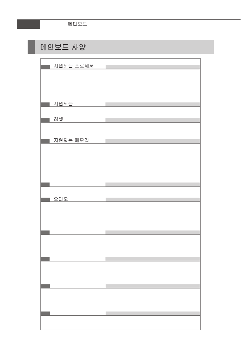
메인보드 사양
지원되는 프로세서
- Intel® CoreTM 2 Extreme/Quad/Duo, Pentium® Dual-Core, Celeron® 및
LGA775 패키지의 프로세서
- Intel® Yorkeld, Wolfdale, Conroe 패밀리 이상 지원
*(CPU에 대한 최신 정보는 http://global.msi.com.tw/index php?func=
cpuform 참조)
지원되는 FSB
- 1600*(OC)/ 1333/ 1066/ 800 MHz
칩셋
- 노스 브릿지: Intel® Eaglelake P45 칩셋
- 사우스 브릿지: Intel® ICH10/ ICH10R 칩셋
지원되는 메모리
- 4 DDR3 DIMM이 DDR3 **1600 (OC) /1333/1066/800 MHz 지원
SDRAM(8GB Max 지원, Intel 웹 사이트 참조)
- 또는 4 DDR2 DIMM이 DDR2 **1066 (OC) / 800/ 667 SDRAM 지원 (최
대 16GB)
**(호환 가능한 부품에 대한 자세한 내용은 http://global.msi.com.tw/in-
dex.php?func=testreport 참조)
LAN
- Realtek 8111C에 의해 PCIE LAN 10/100/1000 고속 이더넷 지원
오디오
- Realtek® ALC888에 의해 통합된 칩
- 잭 감지 기능이 있는 플렉시블 8채널 오디오
- Azalia 1.0 규격 준수
- Microsoft Vista Premium 사양 충족
IDE
- IDE 포트 1개 (JMicron JMB363에 의해 제어되는)
- Ultra DMA 66/100/133 모드 지원
- PIO, 버스 마스터 작동 모드 지원
SATA
- ICH10/ ICH10R에 의한 SATAII 포트 6개 (SATA1~6)
- JMicron JMB363에 의한 SATA II 포트 2개 (SATA7, SATA8)
- 최대 3Gb/s의 저장 및 데이터 전송 지원
RAID
- SATA1~6이 ICH10R에 의해 Intel 매트릭스 저장 기술 (AHCI + RAID
0/1/5/10) 지원
- SATA 7~8은 JMicron JMB363에 의해 RAID 0/1 지원
IEEE1394 (옵션)
- JMicron JMB381에 의해 통합된 칩
- 포트 최대 2개까지 지원 (후면 1개, 전면 1개)
Kr-2

FDD
- 플로피 포트 1개
- 360KB, 720KB, 1.2MB, 1.44MB 및 2.88MB의 FDD 1개 지원
커넥터
후면 패널
- PS/2 마우스 포트 1개
- PS/2 키보드 포트 1개
- 병렬 포트 1개
- COM 포트 1개
- CMOS 지우기 버튼 1개
- USB 2.0 포트 4개
- 1394 포트 1개 (옵션)
- LAN 잭 1개
- 플렉시블 오디오 잭 6개
온보드 핀헤더/커넥터
- USB 2.0 핀헤더 4개
- IEEE 1394 핀헤더 1개 (옵션)
- 섀시 침입 커넥터 1개
- SPDIF 출력 핀헤더 1개
- CD 입력 커넥터 1개
- 전면 오디오 핀헤더 1개
- TPM 모듈 핀헤더 1개 (옵션)
- 전원 버튼 1개
- 리셋 버튼 1개
- 하드웨어 오버클록 FSB 스위치
- 직렬 포트 핀헤더 1개
TPM (옵션)
- TPM 지원
슬롯
- PCI Express x16 슬롯 1개가 PCIE 2.0 규격 지원
- PCI Express x1 슬롯 1개
- PCI 슬롯 3개
폼 팩트
- ATX (30.5cm X 24.4cm)
장착
- 장착 구멍 9개
한국어
Kr-3
MS-7532 메인보드
ON
1 2 3
RESET
OC_SW1, p.Kr-15
SYSFAN1, p.Kr-10
PCI Express 슬롯,
p.Kr-15
마우스/키보드,
p.Kr-16
JPWR2,
p.Kr-14
직렬 포트,
p.Kr-16
병렬 포트,
p.Kr-16
CMOS 지우기
버튼, p.Kr-16
CPU,
p.Kr-5
1394 포트,
p.Kr-17
USB 포트,
p.Kr-17
DDR2,
p.Kr-7
LAN,
p.Kr-17
라인 입력
라인 출력
마이크
CPUFAN1,
p.Kr-10
RS 출력
CS 출력
SS 출력
오디오 포트,
p.Kr-17
JPWR1, p.Kr-14
DDR3, p.Kr-7
SYSFAN2, p.Kr-10
IDE1, p. Kr-10
PCI 슬롯, p. Kr-15
Kr-4
JAUD1,
p.Kr-12
JCD1,
p.Kr-13
SPDIF1,
p.Kr-12
FDD1,
p.Kr-10
J1394_1,
p.Kr-11
JCOM1,
p.Kr-13
빠른 P45-8D 시리즈 부품 설명서
(MS-7532 v1.X) 메인보드
JTPM1,
p.Kr-13
JCI1, p.Kr-13
SATA1~8, p.Kr-11
JUSB1~4, p.Kr-12
RESET1/POWER1,
p.Kr-14
JFP2/1, p.Kr-11

CPU (중앙 처리 장치) : CPU
메인보드가 Intel® 프로세서를 지원합니다. 메인보드는 CPU를 간편하게 설치하기 위해 소켓
775라고 하는 CPU 소켓을 사용합니다. CPU 쿨러가 없는 경우, 컴퓨터를 켜기 전에 판매점
에 문의하십시오.
CPU에 대한 최신 정보는 http://global.msi.com.tw/index.php?func=cpuform 참조
중요 사항
중요 사항
과열
과열은
CPU
각 팬이 제대로 작동하는지 항상 확인하십시오. 열이 잘 발산되도록
사이에 서멀 페이스트 (또는 서멀 테이프) 를 고르게 바르십시오
CPU
CPU
트에서 뽑아
오버클로킹
이 메인보드는 오버클로킹 기능을 지원하도록 디자인되었습니다. 그러나 오버클로킹이
진행되는 동안 부품이 이러한 비정상적인 설정을 견뎌낼 수 있는지 확인하십시오. 제품
사양을 초과하는 범위에서 작동시키지 마십시오. 당사는 올바르지 않은 작동이나 제품
사양을 초과한 범위에서 사용하여 발생한 손상 또는 위험은 보증하지 않습니다.
와 시스템을 심각하게 손상시킬 수 있습니다
교체
교체 시, 항상
ATX
CPU
전원을 끄거나 먼저 전원 공급장치의 전 코드를 접지된 콘센
의 안전을 확보하십시오
.
. CPU
가 과열되지 않도록 냉
CPU
.
와 방열판
한국어
Kr-5
MS-7532 메인보드
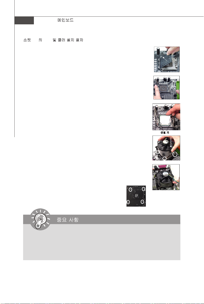
소켓 775의 CPU 및 쿨러 설치 절차
1. CPU 소켓에는 접촉에 의한 손상을 방지하는 플라스틱 캡이 있습니다. CPU
를 설치하기 전에, 항상 캡으로 소켓을 덮어 소켓 핀을 보호하십시오.
2. 캡을 레버 힌지 쪽으로부터 제거하십시오.
3. 소켓의 핀이 드러납니다.
4. 로드 레버를 엽니다.
5. 로드 레버를 위로 올리고 로드 플레이트를 엽니다.
6. CPU 방향이 올바로 맞춰졌는지 확인한 다음, CPU를 소켓 하우징 프레
임에 내려 놓습니다. CPU 베이스의 가장자리를 잡으십시오. 정렬 키가
맞춰졌는지 유의하십시오.
7. CPU가 소켓에 제대로 앉혀졌는지 육안으로 검사합니다. 그렇지 않은
경우, CPU를 수직 방향으로 들어 올린 다음 다시 설치합니다.
8. 로드 플레이트로 패키지를 덮습니다.
9. 로드 레버를 로드 플레이트 위로 살짝 누른 다음, 리텐션 탭 아래의 훅
을 사용하여 레버를 고정합니다.
10. 메인보드의 구멍을 쿨러와 맞춥니다. 4개의 클립이 메인보드의 구멍에
완전히 박힐 때까지 쿨러를 누릅니다.
11. 잠금 스위치를 돌려 훅을 잠급니다 (스위치에 표시된 올바른 방향참
조).
12. 메인보드를 뒤집어 클립 엔드가 올바로 끼워졌는지 확인합니다.
정렬 키
중요 사항
중요 사항
1. BIOS에서 CPU
2. CPU
가 설치되어 있지 않은 경우, 손상되지 않도록 항상 플라스틱 캡으로
핀을 보호하십시오
3.
이 절에 표시된 메인보드 사진은
입니다. 메인보드의 외관은 구입한 모델에 따라 다릅니다
상태를 읽습니다
.
.
CPU/
쿨러 설치를 보여줄 목적으로만 사용된 사진
Kr-6
CPU
소켓
.

메모리
DIMM 슬롯은 메모리 모듈을 설치하는 데 사용됩니다.
DDR3 메모리 모듈은 DDR2과 서로 교환되지 않으며, DDR3 표준은 역호환이 되지 않습니
다. 항상 DDR3 메모리 모듈을 슬롯 (DIMM3/4/7/8) 에 , DDR2 메모리 모듈은 DDR2 슬롯
(DIMM1/2/5/6)에 설치해야 합니다.잘못 설치하면 메인보드가 손상될 수 있습니다. DDR2 및
DDR3 메모리 모듈을 동시에 설치할 경우, 시스템을 부팅할 수 없습니다.
호환 가능한 부품에 대한 자세한 내용은 http://global.msi.com.tw/index.php?func=testreport
를 참조하십시오.
DDR2 (녹색/오렌지색)
240 핀, 1.8V
64x2=128 핀 56x2=112 핀
DIMM1/2/5/6는 DDR2 메모리 모듈용임
DDR3 (파란색/핑크색)
240 핀, 1.5V
72x2=144 핀48x2=96 핀
DIMM3/4/7/8는 DDR3 메모리 모듈용임
듀얼 채널 모드 배포 규칙
듀얼 채널 모드에서는 메모리 모듈이 2개의 데이터 버스 회선을 동시에 사용하여 데이터를
전송 및 수신할 수 있습니다. 듀얼 채널 모드를 활성화하면 시스템 성능이 향상됩니다. 다음
그림에서 듀얼 채널 모드의 배포 규칙을 참조하십시오.
DDR2에 대한 듀얼 채널 모드 배포 규칙:
DIMM1
DIMM2
DIMM3
DIMM4
DIMM5
DIMM6
DIMM7
DIMM8
DIMM1
DIMM2
DIMM3
DIMM4
DIMM5
DIMM6
DIMM7
DIMM8
설치됨
비어 있음
한국어
Kr-7

MS-7532 메인보드
DIMM1
DIMM2
DIMM3
DIMM4
DIMM5
DIMM6
DIMM7
DIMM8
DDR3에 대한 듀얼 채널 모드 배포 규칙:
DIMM1
DIMM2
DIMM3
DIMM4
DIMM5
DIMM6
DIMM7
DIMM8
DIMM1
DIMM2
DIMM3
DIMM4
DIMM5
DIMM6
DIMM7
DIMM8
DIMM1
DIMM2
DIMM3
DIMM4
DIMM5
DIMM6
DIMM7
DIMM8
Kr-8
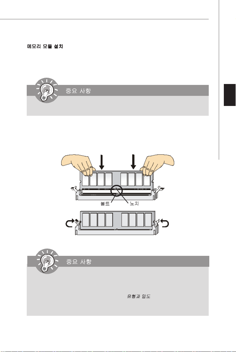
메모리 모듈 설치
1. 메모리 모듈은 중앙에 노치가 하나만 있으며, 오른쪽 방향으로만 맞습니다.
2. 메모리 모듈을 DIMM 슬롯에 수직으로 끼웁니다. 그리고 나서 메모리 모듈 위의 골든 핑
거가 DIMM 슬롯에 깊이 삽입될 때까지 밀어 넣습니다. 메모리 모듈이 제자리를 잡으면,
DIMM 슬롯의 양쪽에 있는 플라스틱 클립이 자동으로 닫힙니다.
중요 사항
중요 사항
메모리 모듈이
3. 메모리 모듈이 양쪽에 있는 DIMM 슬롯 클립에 의해 제자리에 잠가졌는지 수동으로 확인
하십시오.
DIMM
슬롯에 제대로 삽입되면 골든 핑거가 거의 보이지 않습니다
.
한국어
볼트
중요 사항
중요 사항
- DDR3
메모리 모듈은
습니다
. DDR3
모듈을
DDR2 스롯 (DIMM1/2/5/6)
-
듀얼 채널 모드에서, 다른 채널
치했는지 확인하십시오
-
성공적인 시스템 부팅을 하려면, 먼저 메모리 모듈을
DDR2
메모리 모듈을 항상
과 서로 교환되지 않으며
DIMM
.
DDR3 DIMM 슬롯 (DIMM3/4/7/8) 에, DDR2
에 설치해야 합니다
슬롯에 유형과 밀도가 동일한 메모리 모듈을 설
노치
, DDR3
.
DIMM1/ DIMM3
표준은 역호환이 되지 않
메모리
에 끼우십시오
Kr-9
.

MS-7532 메인보드
커넥터, 점퍼, 버튼, 스위치, 슬롯
팬 전원 커넥터 : CPUFAN1, SYSFAN1~2
팬 전원 커넥터는 +12V의 시스템 냉각 팬을 지원합니다. CPU FAN은 Smart FAN 기능을 지
원합니다. 전선을 커넥터에 연결할 때, 항상 빨간색 전선이 양극으로서 +12V에 연결되어야
하고, 검은색 전선은 접지선으로서 GND에 연결되어야 합니다. 메인보드에 시스템 하드웨어
모니터 칩셋 온보드가 있는 경우, CPU 팬 제어를 활용하기 위해 속도 센서가 있는 특별히 디
자인된 팬을 사용해야 합니다.
센서
+12V
GND
제어
CPUFAN1
중요 사항
중요 사항
1.
프로세서의 공식 웹 사이트에서 권장
각 팬을 문의하십시오
2. CPUFAN1
제어하는
3. 3 또는 4
은 팬 제어를 지원합니다. 실제
Dual Core Center
핀 전원 커넥터로 설치된 팬 쿨러는 모두
.
유틸리티를 설치할 수 있습니다
센서
+12V
GND
SYSFAN1
CPU
팬을 참조하거나 판매점에 올바른
CPU
온도에 따라
GND
+12V
NC
SYSFAN2
CPU
.
CPUFAN1
에서 사용할 수 있습니다
CPU
냉
팬 속도를 자동으로
.
플로피 디스크 장치 커넥터: FDD1
이 커넥터는 360KB, 720KB, 1.2MB, 1.44MB 또는 2.88MB 플로피 디스크 드라이브를 지원
합니다.
IDE 커넥터: IDE1
이 커넥터는 IDE 하드 디스크 드라이브, 광학 디스크 드라이브 및 기타 IDE 장치를 지원합
니다.
중요 사항
중요 사항
동일한 케이블에 2개의
드라이브를 별도로 구성해야합니다. 점퍼 설정 방법은 공급업체가 제공한
설명서를참조하십시오
IDE
장치를 설치하는 경우, 점퍼 설정으로 마스터/슬레이브에
.
IDE
장치의
Kr-10

직렬 ATA 커넥터: SATA1~8
이 커넥터는 고속의 직렬 ATA 인터페이스 포트에 사용됩니다. 각 커넥터는 하나의 직렬 ATA
장치에 연결할 수 있습니다.
중요 사항
중요 사항
직렬
ATA
케이블을
90
도로 꺾지 마십시오. 그럴 경우 전송 중 데이터가 손실될 수 있
습니다.
전면 패널 커넥터: JFP1, JFP2
이 커넥터는 전면 패널 스위치 및 LED에 대한 전기 연결에 사용됩니다. TJFP1은 Intel® Front
Panel I/O Connectivity Design Guide를 준수합니다.
전원
전원
스위치
2
1
LED
HDD
LED
JFP1
리셋
스위치
10
9
2
1
스피커
+
전원
LED
JFP2
+
-
8
7
한국어
IEEE1394 커넥터 (녹색) : J1394_1 (옵션)
이 커넥터를 사용하여 옵션인 IEEE1394 브래킷을 통해 IEEE1394 장치를 연결할 수 있습
니다.
IEEE1394 브래킷
(옵션)
TPA-접지TPB-
케이블 전원er
접지
TPA+
접지
TPB+
10
9
키(핀 없음)
케이블 전원
2
1
Kr-11

MS-7532 메인보드
전면 USB 커넥터 (노란색) : JUSB1~4
Intel® I/O Connectivity Design Guide를 준수한 이 커넥터는 USB HDD, 디지털 카메라, MP3 플레
이어, 프린터, 모뎀 등과 같은 고속의 USB 인터페이스 주변 장치를 연결하는 데 적합합니다.
10
USBOC
GND
USB1+
USB1-
VCC
VCC 및 GND
9
키 (핀 없음)
GND
USB0+
USB0-
VCC
1 2
중요 사항
중요 사항
의 핀은 손상을 방지하기 위해 올바로 연결되어야 합니다
USB 2.0 브래킷
(옵션)
.
S/PDIF 출력 커넥터: SPDIF1
이 커넥터는 디지털 오디오 전송을 위해 S/PDIF (Sony & Philips Digital Interconnect Format)
인터페이스를 연결하는 데 사용됩니다.
SPDIF_출력
VCC
GND
SPDIF 브래킷 (옵션)
전면 패널 오디오 커넥터: JAUD1
이 커넥터를 사용하여 전면 패널 오디오를 연결할 수 있으며, 이 커넥터는 Intel® Front Panel
I/O Connectivity Design Guide를 준수합니다.
Kr-12
2
1
접지
NC
MIC _L
MIC _R
MIC_JD
NC (핀 없음)
앞면_JD
라인 출력_R
라인 출력_JD
10
라인 출력_L
9

CD 입력 커넥터: JCD1
이 커넥터는 외부 오디오 입력용으로 제공됩니다.
GND
L
R
섀시 침입 커넥터: JCI1
이 커넥터는 섀시 침입 스위치 케이블에 연결됩니다. 섀시가 열리는 경우, 섀시 침입 메커니
즘이 활성화됩니다. 시스템이 이 상태를 기록하고 화면에 경고 메시지를 표시합니다. 경고를
지우려면 BIOS 유틸리티에서 레코드를 지워야 합니다.
CINTRU
1
2
GND
직렬 포트 커넥터: JCOM1
이 커넥터는 16550A 고속 통신 포트로서 16 바이트의 FIFO를 송수신합니다. 직렬 장치를 연
결할 수 있습니다.
2
1
DCD
SOUT
접지
9
RI
RTS
CTS
SIN
DSR
DTR
TPM 모듈 커넥터: JTPM1 (옵션)
이 커넥터는 TPM (Trusted Platform Module) 모듈 (옵션) 에 연결됩니다. 자세한 내용과 사용
법은 TPM 보안 플랫폼 설명서를 참조하십시오.
한국어
SIRQ
3Vdual / 3V_STB
VCC3
VCC5
2
1
LCLK
LAD0
LAD1
LRST#
키 (핀 없음)
GND
GND
14
13
LAD2
LAD3
LFRAME#
Kr-13

MS-7532 메인보드
전원 공급장치 연결
전원 공급장치 커넥터를 끼우기 전에 모든 구성요소가 올바르게 설치되어 있어야 손상이
생기지 않습니다. 메인보드의 안정적 작동을 위해 메인보드의 모든 전원 커넥터는 ATX 전
원 공급장치에 연결해야 하며 함께 작동해야 합니다.
ATX 24핀 전원 커넥터: JPWR1
이 커넥터를 사용하여 ATX 24핀 전원 공급장치를 연결할 수 있습니다. aTX 핀 전원 공급장
치를 연결하려면, 전원 공급장치의 플러그가 올바른 방향으로 삽입되었는지, 핀이 정렬되었
는지 확인하십시오. 그리고 나서 전원 공급장치를 커넥터 안쪽으로 꽉 맞게누릅니다. 원하는
경우 20핀 ATX 전원 공급장치를 사용할 수 있습니다. 20핀 ATX 전원 공급장치를 사용하려면,
전원 공급장치의 플러그를 핀 1 및 핀 13에 연결하십시오.
12
24
+3.3V
+12V
+12V
5VSB
PWR OK
GND
+5V
GND
+5V
GND
+3.3V
+3.3V
GND
+5V
+5V
+5V
NC
GND
GND
GND
PS-ON#
GND
-12V
+3.3V
1
13
ATX 12V 전원 커넥터 (2x2 핀) : JPWR2
12V 전원 커넥터는 CPU에 전원을 공급하는 데 사용됩니다.
4 2
12V
12V
GND
GND
3
1
전원 버튼: POWER1
이 전원 버튼은 시스템을 켜거나 끄는 데 사용됩니다. 버튼을 눌러 시스템을 켜거나 끕니다.
리셋 버튼: RESET1
이 리셋 버튼은 시스템을 리셋하는 데 사용됩니다. 버튼을 눌러 시스템을 리셋하십시오.
RESET
Kr-14

하드웨어 오버클록 FSB 스위치: OC_SW1
스위치 OC_SW1을 변경하여 프로세서 주파수를 증가시키기 위해 FSB를 오버클록할 수 있
습니다. 아래 지시시항에 따라 FSB를 설정하십시오.
Default
1.
스위치를 변경하기 전에 시스템의 전원을 끄십시오
2. HW
오버클로킹으로 인해 부팅하는 동안 시스템이 깨지거나 불안정해질 수 있습니
다. 그럴 경우 스위치를 기본값으로 전환하십시오
3. BIOS
를 설정하여 오버클로킹해도 됩니다
안 시스템이 깨질 수 있습니다. 그럴 경우 시스템을 3번 재부팅하여 기본
을 복원하십시오 자세한 내용은
PCI Express 슬롯 (x16/ x1)
PCI Express 슬롯은 PCI Express 인터페이스 확장 카드를 지원합니다.
PCI (Peripheral Component Interconnect) 슬롯
PCI 슬롯은 LAN 카드, SCSI 카드, USB 카드 및 PCI 규격을 준수하는 기타 애드온 카드를 지
원합니다.
200->266 MHz 200->333 MHz 200->400 MHz
중요 사항
중요 사항
. BIOS
BIOS
설정 장을 참조하십시오
PCI Express x1 슬롯
266->333 MHz
266->400 MHz
333->400 MHz
.
.
오버클로킹으로 인해 부팅하는 동
BIOS
.
PCI Express x16 슬롯
설정
한국어
중요 사항
중요 사항
확장 카드를 추가하거나 제거할 때 먼저 전원 공급장치의 플러그를 뽑으십시오. 점퍼
스위치 또는
을 구성하려면 확장 카드의 설명서를 읽으십시오
BIOS
구성과 같은 확장 카드에 대해 필요한 하드웨어 및 소프트웨어 설정
.
Kr-15
,

MS-7532 메인보드
후면 패널
마우스/키보드
표준 PS/2® 마우스/키보드 DIN 커넥터는 PS/2® 마우스/키보드용입니다.
PS/2 마우스 커넥터 (녹색/ 6핀 피메일)
PS/2 키보드 커넥터 (자주색/ 6핀 피메일)
병렬 포트
병렬 포트는 표준 프린터 포트로서, 확장 병렬 포트 (EPP) 및 확장 성능 병렬 포트 (ECP) 모
드를 지원합니다.
13 1
(25핀 피메일 커넥터)
1425
직렬 포트
이 직렬 포트는 16550A 고속 통신 포트로서 16 바이트의 FIFO를 송수신합니다. 직렬 마우스
또는 기타 직렬 장치를 커넥터에 직접 연결할 수 있습니다.
1 5
(9핀 메일 커넥터)
6 9
CMOS 지우기 버튼
보드에 시스템 구성 데이터를 유지하기 위해 외부 배터리로부터 전원을 공급 받은 CMOS
RAM이 있습니다. CMOS RAM의 경우, 시스템을 켤 때마다 시스템이 OS를 자동으로 부팅
합니다. 시스템 구성을 지우려면, 버튼을 사용하여 데이터를 지우십시오. 버튼을 눌러 데이
터를 지우십시오.
중요 사항
중요 사항
CMOS
데이터를 지우기 전에 시스템의 전원을 껐는지 확인하십시오
.
Kr-16

1394 포트 (옵션)
후면 패널의 IEEE1394 포트는 IEEE1394 장치에 대한 연결을 제공합니다.
LAN
표준 RJ-45 LAN 잭은 Local Area Network (LAN) 연결용입니다. 네트워크 케이블을 이 잭에
연결할 수 있습니다.
LED 색상 LED 상태 조건
끄기 링크가 구축되지 않았습니다.
왼쪽 노란색 켜기 (지속 상태) LAN 링크가 구축되었습니다.
켜기 (밝게 및 펄싱)
녹색 꺼짐 10 Mbit/sec 데이터 속도를 선택했습니다.
오른쪽 켜짐 100 Mbit/sec 데이터 속도를 선택했습니다.
오렌지색 켜짐 1000 Mbit/sec 데이터 속도를 선택했습니다.
컴퓨터가 LAN 상의 다른 컴퓨터와 통신 중입니다.
USB 포트
USB (Universal Serial Bus) 포트는 키보드, 마우스 또는 기타 USB 호환 가능 장치와 같은 USB
장치를 연결하는 데 사용됩니다.
한국어
오디오 포트 커넥터
이 오디오 커넥터는 오디오 장치에 사용됩니다. 오디오 잭의 색상으로 오디오 사운드 효과
를 구별할 수 있습니다.
라인 입력 (파란색) – 라인 입력은 외부 CD 플레이어, 테이프 플레이어 또는 기타 오디오 장
치에 사용됩니다.
라인 출력 (녹색) – 라인 출력은 스피커 또는 헤드폰에 사용되는 커넥터입니다.
마이크 (핑크색) – 마이크는 마이크에 사용되는 커넥터입니다.
RS 출력 (검은색) – 4/5.1/7.1 채널 모드의 뒤쪽 서라운드 출력.
CS 출력 (오렌지색) – 5.1/7.1 채널 모드의 중앙/서브우퍼 출력.
SS 출력 (회색) – 7.1 채널 모드의 측면 서라운드 출력.
Kr-17

MS-7532 메인보드
BIOS 설정
이 장에서는 BIOS 설정 프로그램에 대한 기본 정보를 제공하여 사용자가 최적의 사용을 위해
시스템을 구성할 수 있도록 도와줍니다. 다음의 경우 설정 프로그램을 실행해야 합니다.
* 시스템을 부팅하는 동안 화면에 오류 메시지가 나타나고 BIOS 설정을 실행하도록 요청하
는 경우.
* 사용자 정의된 기능을 사용하기 위해 기본 설정을 변경하려는 경우.
중요 사항
중요 사항
1.
이 장에서 설명되는 각
적으로 업데이트됩니다. 따라서 설명이 최신
로만 사용해야 합니다
2.
부팅 시 메모리 카운트 다음에 나타나는 첫 번째 행의 정보가
대개의 경우 다음과 같은 형식으로 표시됩니다
A7532IMS V1.0 071808,
1
번째 문자는
2~5
번째 자리수는 모델 번호입니다
6
번째 문자는 칩셋 공급업체로서
니다
7~8
번째 문자는 고객으로서
V1.0은 BIOS
071808
.
은 이
BIOS
버전입니다
BIOS
BIOS
범주 아래의 항목은 시스템 성능을 향상하기 위해 계속
.
마커로서
가 발표된 날짜입니다
, A = AMI, W = AWARD, P = PHOENIX
.
, A = AMD, I = Intel, V = VIA, N = Nvidia, U = ULi
, MS =
모든 표준 고객입니다
.
BIOS
와 약간 다를 수 있으며참조용으
BIOS
.
여기에서:
.
.
버전입니다. 이는
입니다
.
입
Kr-18

설정 시작
컴퓨터를 켜면 시스템이 POST (Power On Self Test) 프로세스를 시작합니다. 화면에 아래의
메시지가 표시되면, <DEL> 키를 눌러 설정을 시작합니다.
DEL을 눌러 설정 (SETUP) 을 시작합니다.
사용자가 응답하거나 설정을 입력하기 전에 메시지가 표시되면, 시스템을 껐다가 다시 켜거
나 리셋 버튼을 누릅니다. 또한 <Ctrl>, <Alt> 및 <Delete> 키를 동시에 눌러 시스템을 다시 시
작할 수도 있습니다.
도움말 불러오기
설정 메뉴를 시작한 다음, 처음으로 표시되는 메뉴가 주 메뉴입니다.
주 메뉴
주 메뉴는 변경할 수 있는 설정 기능을 나열합니다. 화살표 키 (↑↓ ) 를 사용하여 항목을 선
택할 수 있습니다. 강조 표시된 설정 기능의 온라인 설명이 화면의 하단에 표시됩니다.
하위 메뉴
오른쪽 그림과 같이 올바른 포인터 기호가 특정 필드의 왼쪽에 표시되
면, 이 필드에서 추가 옵션을 포함한 하위 메뉴를 시작할 수 있다는 것
을 의미합니다. 컨트롤 키 (↑↓) 를 사용하여 필드를 강조 표시한 다음
<Enter> 를 누르면<Enter>를 눌러 하위 메뉴를 시작합니다. 그런 다음
컨트롤 키를 사용하여 값을 입력하고 하위 메뉴 내에서 필드 간을 이동
합니다. 주 메뉴로 돌아가려면, <Esc > 를 누르기만 하면 됩니다.
일반 도움말 <F1>
BIOS 설정 프로그램은 일반 도움말 화면을 제공합니다. 간단히 <F1> 을 누르기만 하면 어느
메뉴에서든지 이 화면을 불러낼 수 있습니다. 도움말 화면은 사용할 수 있는 적절한 키와 강
조 표시된 항목에 대해 선택할 수 있는 항목을 나열합니다. <Esc> 를 누르면 도움말 화면이
종료됩니다.
한국어
Kr-19

MS-7532 메인보드
The Main Menu (주 메뉴)
AMI® 또는 AWARD® BIOS CMOS 설정 유틸리티에 들어가면 주 메뉴가 화면에 표시됩니다. 주
메뉴에서 설정 기능 열 개 및 종료 방법 두 가지 중에서 선택할 수 있습니다. 화살표 키를 사용하
여 항목 중 하나를 선택한 다음 <Enter> 를 눌러 하위 메뉴를 수락하거나 또는 시작합니다.
Standard CMOS Features (표준 CMOS 기능)
이 메뉴를 사용하여 시간, 날짜 등과 같은 기본 시스템 구성을 처리합니다.
Advanced BIOS Features (고급 BIOS 기능)
이 메뉴를 사용하여 특별 고급 기능의 항목을 설정합니다.
Integrated Peripherals (통합된 주변 장치)
이 메뉴를 사용하여 통합된 주변 장치의 설정을 지정합니다.
Power Management Setup (전원 관리 설정)
이 메뉴를 사용하여 전원 관리의 설정을 지정합니다.
H/W Monitor (H/W 모니터)
이 항목은 PC의 상태를 표시합니다.
BIOS Setting Password (BIOS 설정 암호)
이 메뉴를 사용하여 암호를 설정합니다.
Cell Menu (셀 메뉴)
이 메뉴를 사용하여 주파수/전압 제어 및 오버클로킹의 설정을 지정합니다.
USER SETTINGS (사용자 설정)
이 메뉴를 사용하여 설정을 BIOS CMOS로/BIOS CMOS로부터 저장하거나 로드합니다.
Load Fail-Safe Defaults (장애시 안전 기본값 로드)
이 메뉴를 사용하여 안정된 시스템 성능을 위해 BIOS 공급업체가 설정한 기본값을방문하
십시오.
Load Optimized Defaults (최적 기본값 로드)
이 메뉴를 사용하여 특별히 메인보드 최적의 성능을 위해 메인보드 제조업체가 설정한기본
값을 로드합니다.
Save & Exit Setup (저장 및 설정 종료)
CMOS에 변경사항을 저장하고 설정을 종료합니다.
Exit Without Saving (저장하지 않고 종료)
모든 변경사항을 취소하고 설정을 종료합니다.
Kr-20

BIOS 설정 유틸리티를 시작할 때, 일반적 사용의 경우 다음 절차를 따르십시오.
1. Load Optimized Defaults (최적 기본값 로드) : 컨트롤 키 ( ↑ ↓ ) 를 사용하여 Load Optimized Defaults (최적 기본값 로드) 필드를 강조 표시한 다음 <Enter>를 누르면 아래와 같
은 메시지가 표시됩니다.
OK (확인) 을 선택하고 Enter 를 누르면 최적의 시스템 성능을 위한 기본 설정이 로드됩니
다.
2. Setup Date/ Time (날짜/시간 설정) : Standard CMOS Features (표준 CMOS 기능) 을 선
택한 다음 <Enter>를 눌러서 표준 CMOS 기능 메뉴로 들어갑니다. 날짜, 시간 필드를 조정
합니다.
3. Save & Exit Setup (저장 및 설정 종료) : 컨트롤 키 ( ↑ ↓ ) 를 사용하여 Save & Exit Setup
(설정 저장 및 종료) 필드를 강조 표시한 다음 <Enter>를 누르면아래와 같은 메시지가 표시
됩니다.
한국어
이제 OK (확인) 키와 Enter 키를 눌러 구성을 저장한 다음 BIOS 설정 유틸리티를 종료합니
다.
중요 사항
중요 사항
위의 구성은 일반적 사용의 경우에만 해당됩니다
웹사이트의 한국어 설명서를 참조하십시오
. BIOS
.
설정에 대한 세부사항은
MSI
Kr-21

MS-7532 메인보드
4. Cell Menu Introduction (셀 메뉴 소개) : 메인보드를 오버클로킹하려는 고급 사용자를 위
한 메뉴입니다.
중요 사항
중요 사항
사용자가 칩셋에 익숙할 경우에만 이 설정을 변경하십시오.
Current CPU/DRAM Frequency (현재 CPU/DRAM 주파수)
이 항목은 CPU 및 메모리 속도의 현재 클록을 표시합니다. 읽기 전용입니다.
Kr-22

D.O.T Control (D.O.T 제어)
D.O.T. (동적 오버클럭킹 기술) 는 자동 오버클럭킹 기술로서, MSITM가 새롭게 개발한 Dual
CoreCellTM 기술에 속합니다. 이 기술은 프로그램을 실행하는 동안 CPU의 로드 밸런스를
감지하고 최상의 주파수로 자동 조정하는 기능을 갖추고 있습니다. 마더 보드가 시스템이
프로그램을 실행 중이라는 것을 감지하면 자동으로 속도가 높아져서 프로그램을 보다 매끄
럽고 빠르게 실행하도록 만듭니다. 시스템이 잠시 지체되거나 낮은 로딩 밸런스에 머물 경
우 기본 설정을 대신 복구합니다. 일반적으로 동적 오버클로킹 기술은 사용자의 PC가 전반
적인 성능 향상이 필요한 3D 게임, 비디오 프로세스 및 CPU 및 PCIE 주파수와 같이 대용량
의 데이터를 실행할 경우에만 작동됩니다.
중요 사항
중요 사항
동적 오버클로킹 기술이 수동 오버클로킹에 비해 안정적이지만 기본적으로 여전히 위
험 요소가 남아 있습니다. 우선
도록 하는 것이 바람직합니다
는 경우 오버클로킹 옵션 레벨을 낮추는 것이 좋습니다. 어쨌든 수동으로 오버클로킹
해야 할 경우 우선 동적 오버클로킹을 비활성화해야 합니다
Intel EIST
향상된 Intel SpeedStep 기술로 인해 배터리 또는 AC 전원 중 어떤 방식으로 컴퓨터를 실행
되느냐에 따라마이크로프로세서의 성능 레벨을 설정할 수 있습니다. 이 speedstep 기술을
지원하는 CPU를 설치하면 이 필드가 표시됩니다.
Adjust CPU FSB Frequency (CPU FSB 주파수 조정) (MHz)
CPU FSB 주파수 조정에 사용딥니다.
Adjust CPU Frequency (CPU 주파수 조정) (MHz)
이 항목은 조정된 CPU 주파수를 표시합니다 (FSB x 비율). 읽기 전용입니다.
CPU/
메모리 모튤이 정기적으로 오버클로킹할 수 있
. PC
가 불안정하게 보이거나이에 부수적으로 재부팅되
.
한국어
Advance DRAM Conguration (고급 DRAM 구성)
<ENTER> 키를 눌러 하위 메뉴로 들어가면 다음 화면이 나타납니다.
MEMORY-Z (메모리-Z)
<ENTER> 키를 눌러 하위 메뉴로 들어가면 다음 화면이 나타납니다.
Kr-23

MS-7532 메인보드
DIMM1 Memory SPD Information (DIMM1 메모리 SPD 정보)
<ENTER> 키를 눌러 하위 메뉴로 들어가면 다음 화면이 나타납니다.
DIMM 1/2/3/4 메모리 SPD 정보 (DIMM 1/2/3/4 Memory SPD Information)
이 항목은 메모리 타입, 최대 대역폭, 제조업체, 부품 번호, 일련 번호, SDRAM 사
이클 타임, DRAM TCL, DRAM TRCD, DRAM TRP, DRAM TRAS, DRAM TRFC,
DRAM TWR, DRAM TWTR, DRAM TRRD 및 DRAM TRTP 등과 같은 현재 DIMM
메모리 속도 정보의 현재 상태를 표시합니다. 읽기 전용입니다.
CAS Latency (tCL) (CAS 대기 시간)
이렇게 되면 SDRAM이 읽기 명령을 받아서 이 명령을 시작하기 전에 (클록 사이클의)
타이밍 지연을 결정하는 CAS 대기 시간을 제어합니다.
tRCD
DRAM이 재충전되면 행과 열이 따로 분리됩니다. 이 설정 항목을 사용하면 RAS (열 주
소) 에서 CAS (행 주소) 로의 변환 타이밍을 결정할 수 있습니다. 클록 사이클이 짧을수
록 DRAM 성능이 빨라집니다.
tRP
이 설정은 재충전할 수 있는 RAS 사이클 수를 제어합니다. DRAM 재충전 이전에
RAS가 충전 시간을 충분히 갖지 못할 경우, 충전이 불충분해서 DRAM이 데이터를 보
존하지 못할 수 있습니다. 이 항목은 시스템에 동기화 DRAM이 설치된 경우에만 적용
됩니다.
tRAS
이 설정은 RAS가 메모리 셀로부터 읽거나 메모리 셀에 쓰는 데 걸리는 시간을 결정합
니다.
Kr-24
Advanced Memory Setting (고급 메모리 설정)
[자동 (Auto)] 로 설정하면 BIOS에 의해 고급 메모리 타이밍을 자동으로 판별할 수 있
습니다.
FSB/DRAM Ratio (FSB/DRAM 비율)
이 항목을 사용하면 메모리에 대한 FSB 비율을 조정할 수 있습니다.
Adjust DRAM Frequency (DRAM 주파수 조정) (MHz)
이 항목은 DRAM 주파수를 표시합니다. 읽기 전용입니다.
Adjust PCI Frequency (PCI 주파수 조정)
이 항목을 사용하여 PCI 주파수 (MHZ) 를 선택할 수 있습니다.
Auto Disable DIMM/PCI Frequency (DIMM/PCI 주파수 자동 해제)
[사용 (Enabled)] 으로 설정하면 시스템이 빈 DIMM 및 PCI 슬롯에서 클록을 제거 (전원이 꺼
짐)하여 전자파 장애 (EMI) 를 최소화할 수 있습니다. 이 항목은 메모리, FSB 및 칩셋의 전원
상태를 표시합니다. 읽기 전용입니다.
CPU Voltage / CPU GTL REF0 / CPU GTL REF1 / DRAM Voltage (V)/ DDR_VREF_
CA/DA_A/B / NB Voltage / MCH Voltage (V)/ MCH GTL REF / VTT FSB Voltage / ICH
Voltage (V)
이 항목은 메모리, FSB 및 칩셋의 전원 상태를 표시합니다. 읽기 전용입니다.
Spread Spectrum (대역 확산)
메인보드의 클록 생성기가 펄스화되면 펄스의 극치값 (스파이크) 이 전자파 장애를 일으킵니
다. 대역 확산 기능은 펄스 조절로 생성된 EMI를 줄여줌으로써 그 결과 펄스의 스파이크가 평
탄한 곡선으로 줄어듭니다. EMI에 문제가 없는 경우, 시스템 안전성 및 성능을 최적화할 수
있도록 설정을 사용 안함 상태로 둡니다. 그러나 EMI로 인해 문제가 발생할 경우, EMI 감소를
위해 사용으로 설정하십시오. 사소한 지터조차도 클록 속도를 일시적으로 상승시키면 오버클
로킹한 프로세스를 고정시키는 원인이 될 수 있으므로 오버클로킹을 진행하는 동안 대역 확
산을 반드시 사용 안함으로 설정해야 합니다.
중요 사항
중요 사항
1. EMI
문제가 발생하지 않을 경우 최적의 시스템 안정성 및 성능을 위해 [사용 안
함]으로 설정합니다. 그러나
역 확산 값을 선택하십시오
2.
대역 확산 값이 클수록
합한 대역 확산 값은 해당 지역의
3.
사소한 지터조차도 클록 속도를 일시적으로 상승시키면 오버클로킹한 프로세스를
고정시키는 원인이 될 수 있으므로 오버클로킹을 진행하는 동안 대역 확산을 반드
시 사용 안함으로 설정해야 합니다
EMI
로 인해 문제가 발생할 경우
.
EMI
는 감소되지만 시스템의 안정성은 저하됩니다. 가장 적
EMI
규정을 참조하십시오
.
, EMI
.
감소를 위해 대
한국어
Kr-25

MS-7532 메인보드
CPU
및 메모리 클럭 오버클럭킹
D.O.T 제어, CPU FSB 주파수 조정, CPU 비율 조정, FSB/메모리 비율은 CPU 및 메모리를
오버클럭킹하기 위한 항목입니다. 자세한 내용은 해당 필드 설명을 참조하십시오.
중요 사항
1. CPU 속도 = CPU FSB
2.
이 마더 보드는 오버클럭킹을 전적으로 지원합니다. 그러나 사용자의 주변장치 및
구성요소가 일부 특수 설정을 견딜 수 있는지 확인하십시오. 생산 사양을 초과하
는 작업은 어떤 경우에도 바람직하지 않습니다. 적절하지 못한 작업으로 인한 위
험이나 손상은 당사의 제품 보증을 받지 못합니다
실패한 오버클럭킹으로부터 시스템을 저장하는 두가지 방법
재부팅
1. 전원 버튼을 눌러 시스템을 세 번 재부팅합니다. 전류가 다른 장치나 구성요소에 영향
을 미치지 않도록 주의하십시오. 그러기 위해서 각각의 재부팅 사이에 10초 이상의 간
격을 두는 것이 좋습니다.
2. 네 번째 재부팅 시 BIOS가 이전 오버클럭킹이 실패했음을 판별하고 자동으로 기본 설
정으로 돌아갑니다. 화면에 다음 메시지가 나타나면 아무 키나 눌러 시스템을 평소대
로 부팅하십시오.
주파수
* CPU
비율
.
...
Warning !!! The previous overclocking had failed,
and system will restore its defaults setting,
Press any key to continue.......
CMOS 지우기
- 메인보드 후면 패널의 CMOS 버튼을 눌러서 CMOS 데이터를 지웁니다.
Kr-26

소프트웨어 정보
메인보드 패키지에 들어 있는 드라이버/유틸리티 CD를 꺼내서 CD-ROM 드라이브에 삽입합
니다. 설치는 자동 실행되며, 드라이버나 유틸리티를 클릭하기만 하면 팝업 화면이 설치 완료
를 표시합니다. 드라이버/유틸리티 CD에는 다음이 포함됩니다.
드라이버 메뉴 – 사용 가능한 드라이버를 표시합니다. 원하는 대로 드라이버를 설치한 다음
장치를 활성화합니다.
유틸리티 메뉴 – 메인보드가 지원하는 소프트웨어 응용 프로그램을 표시합니다.
웹사이트 메뉴 – 필요한 웹사이트를 표시합니다.
중요 사항
중요 사항
한국어
최신 드라이버 및
십시오
.
BIOS
로 시스템 성능을 향상시키고 싶다면
MSI
웹사이트를 방문하
Kr-27

This page is intentionally left blank.
viii

P45-8D
取扱説明書
日本語
日本語
Jp-1

MS-7532 マザーボード
マザーボードの仕様
プロセッサー
- LGA775 Intel® Core
とCeleron® プロセッサーをサポート
- Intel® Yorkfield, Wolfdale, Conroe family以上をサポート
*(最新のCPU対応の詳細については弊社のホームページを参照してく
ださい。 http://global.msi.com.tw/index.php?func=cpuform)
TM
2 Extreme/Quad/Duo, Pentium® Dual-Core
対応FSB
- 1600*(OC)/ 1333/ 1066/ 800 MHz
チップセット
- ノースブリッジ: Intel® Eaglelake P45 チップセット
- サウスブリッジ: Intel® ICH10/ ICH10R チップセット
メモリ
- 4 DDR3 DIMMsはDDR3 **1600(OC)/1333/1066/800 SDRAMをサ
ポート(最大8GB搭載可、Intelのホームページをご参照下さい)
- あるいは4 DDR2 DIMMsはDDR2 **1066(OC)/ 800/ 667 SDRAMをサ
ポート(最大16GB搭載可)
**(最新のメモリモジュール対応表は下記のホームページをご参照くだ
さい。http://global.msi.com.tw/index.php?func=testreport)
LAN
- Realtek 8111C PCIE LAN 10/100/1000ファーストイーサネット
オーディオ
- Realtek® ALC888に統合したチップ
- ジャックセンス機能付けの8チャンネルオーディオ
- Azalia 1.0スペック準拠
- Microsoft Vista Premiumスペック準拠
IDE
- 1 IDEポート(JMicron JMB363)
- Ultra DMA 66/100/133モードをサポート
- PIO,バスマスターなどのオペレーションモードをサポート
SATA
- ICH10/ ICH10R 6 SATAIIポート(SATA1~6)
- 2 SATA IIポート(JMicron JMB363) (SATA7, SATA8)
- 最大3 Gb/sまでのデータ転送速度をサポート
RAID
- SATA1~6はIntel Martix Storageテクノロジーをサポート(AHCI +
RAID 0/1/5/10) (ICH10R)
- SATA7~8はRAID 0/ 1をサポート(JMicron JMB363)
IEEE1394(オプション)
- JMicron JMB381に統合したチップ
- 最大2ポートをサポート(リア x 1, フロント x 1)
Jp-2

FDD
- 1 フロッピポート
- 360KB/720KB/1.2MB/1.44MB/2.88MBのFDD、1台の接続が可能
コネクター
バックパネル
- 1 PS/2 マウスポート
- 1 PS/2 キーボードポート
- 1 パラレルポート
- 1 COM ポート
- 1 クリアCMOSボタン
- 4 USB 2.0 ポート
- 1 1394 ポート(オプション)
- 1 LAN ジャック
- 6 オーディオジャック
オンボードピンヘッダー/コネクター
- 4 USB 2.0 ピンヘッダー
- 1 IEEE1394 ピンヘッダー(オプション)
- 1 ケース開放センサーコネクター
- 1 S/PDIF-out ピンヘッダー
- 1 CD-in コネクター
- 1 フロントオーディオピンヘッダー
- 1 TPM モジュールコネクター (オプションオプション)
- 1 電源ボタン
- 1 リセットボタン
- 1 ハードウェアオーバークロックFSBジャンパ
- 1 シリアルポートピンヘッダー
TPM (オプション)
- TPMをサポート
スロット
- PCI Express x16 -1スロット、PCIE 2.0スペックをサポート
- PCI Express x 1 -1スロット
- PCI -3スロット
寸法
- ATX (30.5cm X 24.4cm)
取付穴
- 9 穴
日 本 語
Jp-3

MS-7532 マザーボード
マウス/ キー
ボード,p.Jp-16
OC_SW1, p.Jp-15
SYSFAN1, p.Jp-10
PCI Expressス
ロット,p.Jp-15
パラレルポート
,p.Jp-16
シリアルポート
,p.Jp-16
JPWR2,
p.Jp-14
ON
123
1394ポート
,p.Jp-17
クリアCMOS
ボタン,p.Jp-16
CPU,
p.Jp-5
LAN,
p.Jp-17
USBポート
,p.Jp-17
DDR2,
p.Jp-7
Line-In
Line-Out
Mic
CPUFAN1,
p.Jp-10
RS-Out
CS-Out
SS-Out
オーディ
オポート
,p.Jp-17
JPWR1, p.Jp-14
DDR3, p.Jp-7
SYSFAN2, p.Jp-10
IDE1, p.Jp-10
PCIスロット,
p.Jp-15
JCOM1,
p.Jp-13
JTPM1,
p.Jp-13
JAUD1,
p.Jp-12
JCD1,
p.Jp-13
SPDIF1,
p.Jp-12
FDD1,
p.Jp-10
J1394_1,
p.Jp-11
P45-8Dシリーズのクイックコンポーネントガイド
(MS-7532 v1.X)マザーボード
Jp-4
JCI1, p.Jp-13
SATA1~8, p.Jp-11
JUSB1~4, p.Jp-12
RESET
RESET1/POWER1,
p.Jp-14
JFP2/1, p.Jp-11

CPUに関する注意事項
本製品はIntel®プロセッサーをサポートします。簡単にCPUの着脱が行えるようにSocket
775というCPUソケットを採用します。CPUに冷却ファンが付属していない場合は、その
CPUの発熱量に見合った冷却ファンを予め用意してください。
最新のCPU対応表は下記のホームページからご参照ください。
http://global.msi.com.tw/index.php?func=cpuform
注意!
過熱
CPUが適切に冷却されず、過剰に発熱すると、CPUが破損する場合があ
ります。組み立て後の最初の起動の際に、冷却ファンが正常に動作す
ることを必ず確認してください。
CPUの交換
CPUを交換する場合は必ずコンセントからATX電源コードを抜いた後に
行ってください。通電中のCPUの交換はCPUの破損を招くだけでなく、
感電する危険性があります。
日 本 語
Jp-5

MS-7532 マザーボード
Socket 775 CPU &クーラーのインストール
1. CPUのランドサイドカバー(端子保護カバー)を外します。
2. CPUソケットレバー側からソケット保護カバーをゆっくり外します。
3. CPUソケットのピンが露出した状態になります。
4. レバーを固定プレートのフックから外します。
5. レバーと固定プレートを起こします。
6. CPUのalignment key(位置決めの窪み)とCPUソケットの[出っ張り]を
合わせて、装着する向きを決定します。
7. CPUが正しくソケットに収まっていることを確認してください。
8. 固定プレートをゆっくり下ろします。
9. レバーを下ろしてフックに固定します。
10.CPUクーラーの四隅のピンをマザーボードの固定穴にあわせ、ゆっくり
と固定します。
11.位置が正しいことを確認したら、フックが固定されるまでブッシュピン
を押し込みます。
12.マザーボードを裏返して、裏面に出たブッシュピンの先が
開き、正しくロックできたことを確認します。
alignment key
注意!
1. 使用するCPUにBIOSが対応していることを確認してください。
2. CPUを取り付けない場合は、CPUソケット保護のためプラスチックカバーを必ず
取り付けないてください。
3. 上記の図はCPU取付説明用のため、お手元のマザーボードとは細部が異なる場合が
あります。
Jp-6

メモリ
1
2
Empty
Installed
これらのDIMMスロットはメモリモジュールのインストール用です。
DDR3メモリとDDR2メモリは互いに規格の互換性がありません。本製品ではDDR2モジュー
ルを使用することはできません。DDR3メモリモジュールをDDR3(DIMM3/4/7/8)スロットに
挿入し、DDR2メモリモジュールをDDR2(DIMM1/2/5/6)スロットに挿入してください。間違
うとマザーボードに損傷を招くする恐れがありま す。また、DDR2 & DDR3メモリモジュー
ルを同時にインストールする場合には、システムを起動することができません。
最新のメモリモジュール対応表は下記のホームページを参照ください。
http://global.msi.com.tw/index.php?func=testreport
DDR2 (緑色 & オレンジ)
240-pin, 1.8V
64x2=128 pin 56x2=112 pin
DIMM1/2/5/6はDDR2メモリモジュールのためです。
DDR3 (青色 & ピンク)
240-pin, 1.5V
72x2=144 pin48x2=96 pin
DIMM3/4/7/8はDDR3メモリモジュールのためです。
デュアルチャンネルメモリソケットルール
デュアルチャンネルメモリアクセス方式は、2つのメモリデータバスを同時に使用し てデー
タの読み書きを行うことになり、アクセススピードを向上させます。デュアルチャンネルを
有効にするには、以下の組み合わせでメモリモジュールを装着します。
DDR2のデュアルチャンネルモードのソケットルール:
DIMM1
DIMM2
DIMM3
DIMM4
DIMM5
DIMM6
DIMM7
DIMM8
日 本 語
DIMM1
DIMM2
DIMM3
DIMM4
DIMM5
DIMM6
DIMM7
DIMM8
Jp-7

MS-7532 マザーボード
1
2
3
3
DIMM1
DIMM2
DIMM3
DIMM4
DIMM5
DIMM6
DIMM7
DIMM8
DDR3のデュアルチャンネルモードのソケットルール:
DIMM1
DIMM2
DIMM3
DIMM4
DIMM5
DIMM6
DIMM7
DIMM8
DIMM1
DIMM2
DIMM3
DIMM4
DIMM5
DIMM6
DIMM7
DIMM8
DIMM1
DIMM2
DIMM3
DIMM4
DIMM5
DIMM6
DIMM7
DIMM8
Jp-8

メモリモジュールの装着
1.メモリモジュールには中央付近に切り欠きが設けられており、間違った向きで装着できな
いように設計されています。
2.メモリモジュールを垂直にゆっくり差し込みます。左右のクリップが自動的にメモリモ
ジュールを固定しま す。
注意!
手ごてえが固く手うまく差し込めない場合は無理に力を入れず、左右が傾かないよう水
平を保った状態でゆっくり押し込んでください。
3.手動でメモリモジュールが両側のDIMMスロットクリップに正しくロックさ れ た かど うか をチェッ
クし て ください。
Volt
Notch
注意!
- DDR3メモリとDDR2メモリは互いに規格の互換性がありません。本製品ではDDR2モ
ジュールを使用することはできません。DDR3メモリモジュールをDDR3(DIMM3/4/7/
8)スロットに挿入し、DDR2メモリモジュールをDDR2(DIMM1/2/5/6)スロットに挿入
してください。
- デュアルチャンネルアクセスで有効にするには同一のメモリを2本装着してください。
-メモリスロットはDIMM1/ DIMM3を優先的に使用してください。
日 本 語
Jp-9

MS-7532 マザーボード
コネクター、ジャンパ、ボタン、スイッチ、スロット
ファン電源コネクター: CPUFAN1/ SYSFAN1~2
ファン電源コネクターは +12Vの冷却ファンをサポートします。接続する時に注意しなけ
ればならないのは、赤い線はプラスなので +12Vに、黒い線はアースなので GNDに接続す
ることです。また、本製品のシステムハードウェアモニタ機能を使用する場合はファンの
回転数センサー機能がついたファンを使用する必要があります。
SE NSOR
+1 2V
GND
CONTROL
CPUFAN1
Sensor
+12V
GND
SYSFAN1
GND
+12V
NC
SYSFAN2
注意!
1.CPUメーカーが推奨するファンを参照してください。
2.CPUFAN1はファンコントローラーをサポートします。ユーザーはBIOSのH/W
Monitorメ ニ ューにはファン回転速度を調整でき 、Dual Core Centerユーティリ
ティで目下のCPU温度により自動的にCPUファンの回転数をコントローラーしま
す。
3. 3または4ピンのファンクーラーはCPUFAN1に使用で きます。
FDDコネクター: FDD1
本製品は360KB, 720KB, 1.2MB, 1.44MB及び2.88MBのフロッピーディスクドライブに
対応しています。
IDEコネクター: IDE1
本製品はIDE HDD、光学ディスクドライブなどのデバイスをサポートします。
注意!
ハードディスクを2台使用する場合は、ジャンパピンでマスター/スレープの設定を行
う必要があります。ジャンパ設定についてはハードディスクメーカーが提供するマ
ニュアルを参照してください。
Jp-10
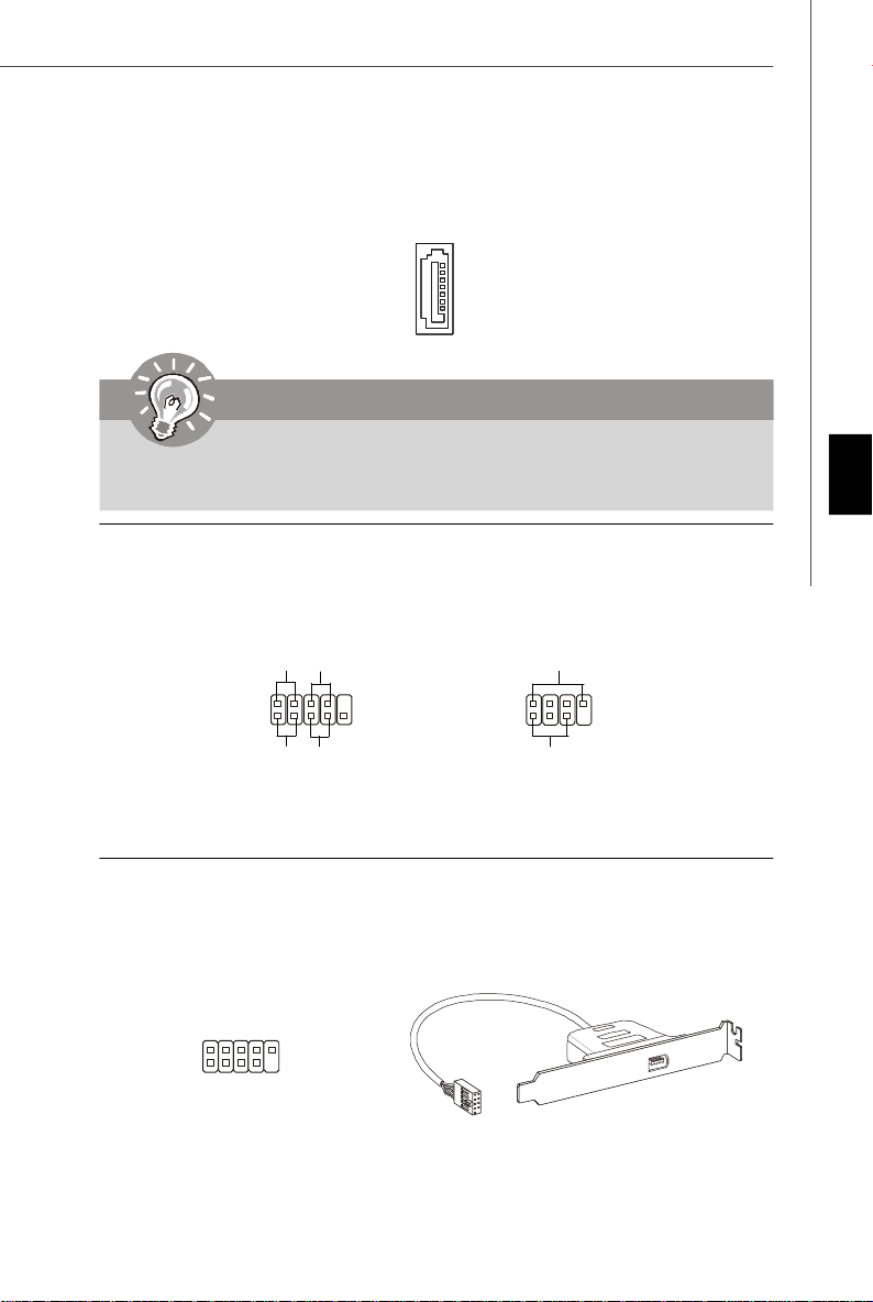
リアルATAコネクター: SATA1~8
このコネクターは高速シリアルATA インターフェイスポートです。一つのコネクターにつ
き、一つのハードディスクを接続することができます。
注意!
シリアルATAケーブルは90度の角度の折り曲げないように注意してください。デー
タ転送時にデータ損失を起こす可能性があります。
フロントパネルコネルター: JFP1, JFP2
本製品にはフロントパネルスイッチやLEDを対象とした電子的接続用に、一つのフロントパ
ネルコネクターが用意されています。JFP1はIntel® Front Panel I/O Connectivity Design
Guideに準拠しています。
Power
Power
LED
2
1
HDD
LED
JFP1
Switch
Reset
Switch
10
9
2
1
Speaker
+
Power
LED
JFP2
+
-
8
7
日 本 語
IEEE1394コネルター(緑色): J1394_1 (オプション)
このコネクターはオプションのIEEE1394ブラケット経由でIEEE1394デバイスを接続しま
す。
IEEE1394 Bracket
(オプション)
TPA-
Ground
TPB-
Cable power
Ground
2
1
10
9
TPA+
TPB+
Ground
Key (no pin)
Cable power
Jp-11
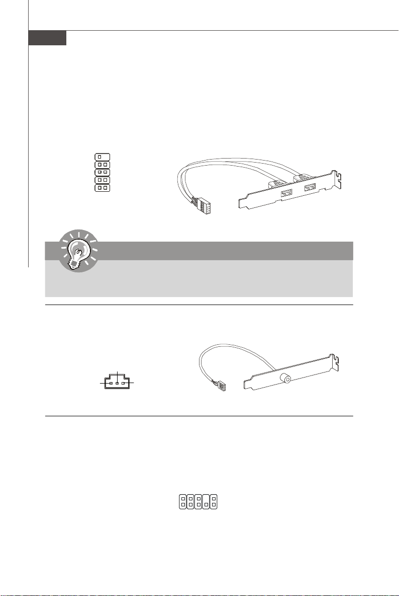
MS-7532 マザーボード
フロントUSBコネクター(黄色): JUSB1~4
本製品にはIntel® I/O Connectivity Design Guideに準拠したUSB 2.0ピンヘッダーが搭載
されています。USBが汎用性が非常に高く、外付けUSB HDDやデジタルカメラ、MP3プレ
イヤー、プリンタなど様々な機器に対応します。
USB 2.0 Bracket
(オプション)
USBOC
GND
USB1+
USB1-
VCC
10
9
1 2
Key (no pin)
GND
USB0+
USB0VCC
注意!
VCCピンとGNDピンは必ず接続してください。接続しない場合、機器に重大な損傷を
及ぼす恐れがあります。
S/PDIF-Outコネクター: SPDIF1
デジタルフォーマットで音声ソースを出力するためのインターフェイスです。5.1チャンネ
ル/7.1チャンネルサウンド音声に対応しています。
SPDIF_out
VCC
フロントパネルオーディオコネクター: JAUD1
フロントパネルオーディオピンヘッダーを使用するとフロンとパネルからのオーディオ出力
が可能になります。ピン配列はIntel® Front Panel I/O Connectivity Design Guideに準拠
しています。
GND
SPDIF Bracket (オプション)
Jp-12
M IC_ J D
NC (N o pi n)
Gr oun d
N C
2
1
MI C _ L
LI NE ou t_ JD
10
9
M IC _R
Fr on t_J D
LIN E ou t_L
LI NE ou t_ R
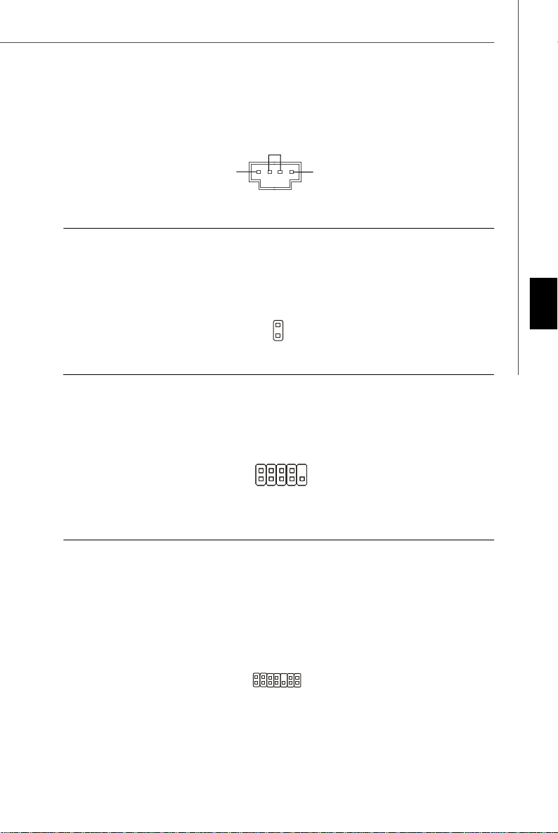
CD-Inコネクター: JCD1
このコネクターはCD-ROMオーディオコネクターを接続します。
GND
L
R
ケース開放センサーコネクター: JCI1
このコネクターには2ピンのケーススイッチを接続します。ケースを開けると開放センサー
がショットします。システムにはこの開放信号が記録され、警告メッセジーが画面に表示さ
れます。警告メッセジーを消すには、BIOSユーティリティーからメッセジーのクリアをか
けます。
CINTRU
1
2
GND
シリアルポートコネクター: JCOM1
モデルによってはJCOM1用のピンヘッダを搭載しています。JCOM1を使 用する場合には別
売りのブラケットが必要です。16550Aチップを採用し、16バイトにてデータ転送を行いま
す。
2
1
DCD
9
RI
RTS
SOUT
Ground
CTS
SIN
DSR
DTR
TPMモジュールコネクター: JTPM1(オプション)
このコネクターはTPM (Trusted Platform Module)モジュール(オプション)を接続します。
詳細についてはTPMセキュリティプラットホームマニュアルを参照してください。
日 本 語
3V dua l / 3V _ST B
VC C3
SIR Q
VC C5
Ke y(n o pin )
GN D
2
1
GN D
14
13
LCLK
LAD0
LAD1
LAD2
LAD3
LR ST#
LF RA ME #
Jp-13

MS-7532 マザーボード
電源コネクターの接続に関する注意
電源コネクターを接続前に、全てのパーツやコネクターが正しく装着されていることを確
認してください。
ATX 24ピン電源コネクター: JPWR1
ATX電源24ピンコネクタを接続します。接続の際にはコネクターの向きに注意して奥まで
しっかり差し込んでください。通常はコネクターのフックの向きを合わせれば正しく接続さ
れます。20ピンのATX電源も使用可能です。その場合には、11, 12, 23 & 24ピンは使用し
ません。
1224
+3.3V
+12V
+12V
5VSB
PWR OK
GND
+5V
GND
+5V
GND
+3.3V
+3.3V
GND
+5V
+5V
+5V
NC
GND
GND
GND
PS-ON#
GND
-12V
+3.3V
1
13
ATX 12V電源コネクター(2x2ピン): JPWR2
この電源コネクターは、CPUに電源を供給します。
4 2
GND12V
12V
GND
13
電源ボタン: POWER1
この電源ボタンはシステムを起動/終了します。
リセットボタン: RESET1
このボタンはシステムをリセットします。
RESET
Jp-14
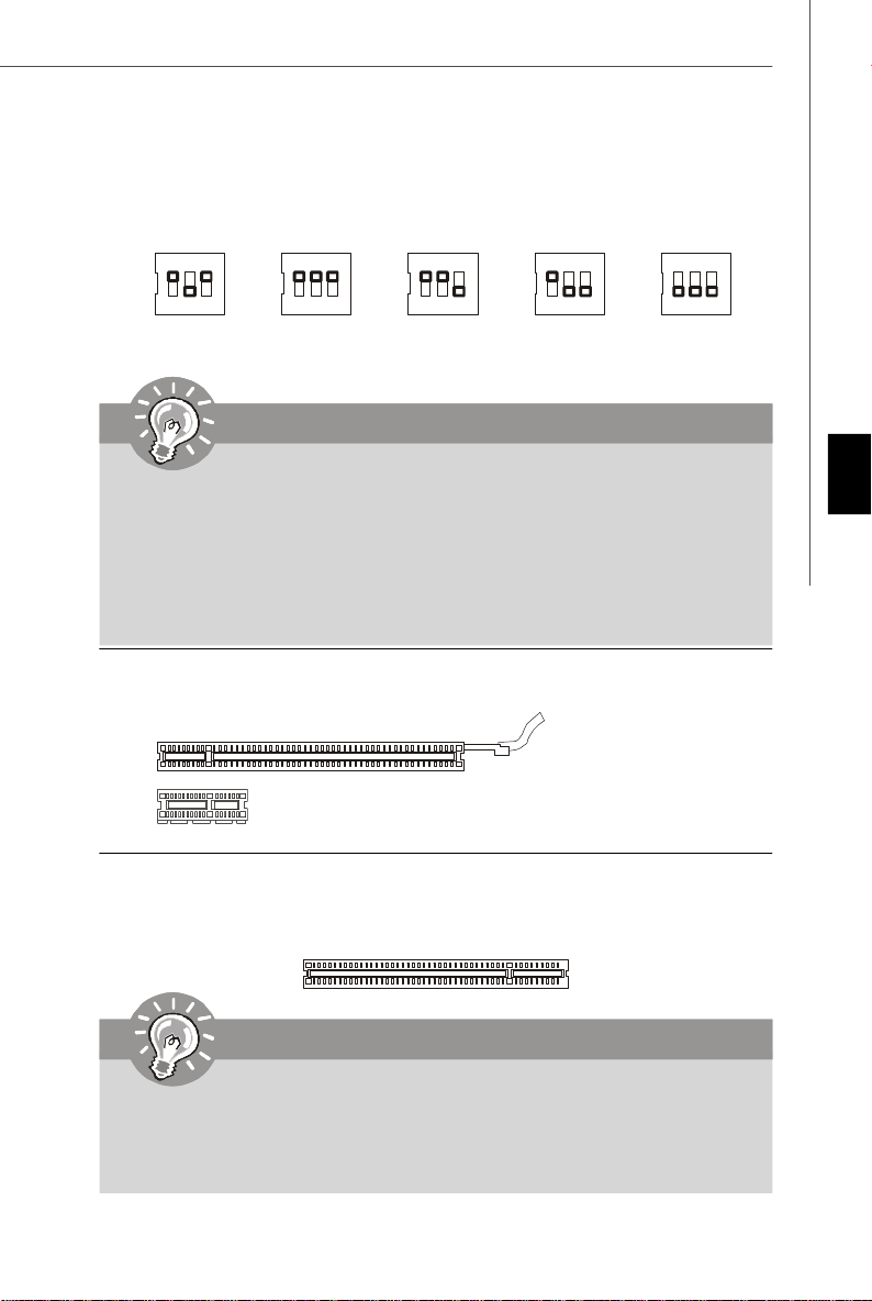
ハードウェアオーバークロックFSBジャンパ: OC_SW1
OC_SW1を変更すると、FSBをオーバークロックしてプロセッサーの周波数を上げることが
できます。以下の説明に従ってFSBを設定して下さい。
ON
123
デフォルト
ON
123
200->266 MHz 200->333 MHz 200->400 MHz
ON
123
ON
123
266->333 MHz
ON
123
266->400 MHz
333->400 MHz
注意!
1. オーバークロックジャンパの設定は、必ずシステムの電源を落としてから行って下
さい。起動中に変更すると、故障の原因になります。
2.システムの起動中に不安定になる場合があります。電源を落として、
ジャンパ設定をデフォルトの状態に戻してください。
3.BIOSにはオーバークロックの設定を行うこともできます。システムの
起動中に不安定になる場合もあります。その時、システムを3回再起
動してデフォルト設定に戻して下さい。詳細については、BIOSの設定
をご参照下さい。
PCI Expressスロット(x16/ x1)
PCI ExpressスロットはPCI Expressインターフェイス拡張カードをサポートします。
PCI Express x 16スロット
PCI Express x 1スロット
PCI (Peripheral Component Interconnect)スロット
PCI スロットは最も汎用性の高い拡張スロットで、対応する様々な拡張カードが発売されて
います。
日 本 語
注意!
拡張カードを挿入したり取り外したりする時は、必ず最初 に電源プラグを抜いてく
ださい。拡張カードについて記述挿入したりされたマニュアルを読んで、ジャン
パ、スイッチ、BIOSなど必要なハードウェア設定、ソフトウェア設定を全て実行し
てください。
Jp-15

MS-7532 マザーボード
バックパネル
マウス/キーボード
マザーボードはPS/2、マウス/キーボードを接続するための標準PS/2、マウス/キーオード
ミニDINコネクターが各一個ずつ設けられています。
PS/2マウスコネクター(緑色/ 6ピンメス)
PS/2キーボードコネクター(紫色/ 6ピンメス)
パラレルポート
パラレルポートはEPPとECP モードをサポートした標準ポートです。
13 1
(25ピンメスコネクター)
1425
シリアルポート
16550Aチップを採用した16バイトFIFOにてデータ転送を行います。このコネクターにシリ
アルマウスまたは他のシリアルデバイスを接続できます。
1 5
(9ピンオスコネクター)
6 9
クリアCMOSボタン
本製品にはCMOS RAMが搭載されており、内蔵電池から電気が供給されることでシステム
情報やBIOSの設定を保持しています。このCMOS RAMに蓄えられたデバイス情報によって、
OSを迅速に起動さ せることが可能になります。システム設定をクリアしたい場合、このボタ
ンを押してデータをクリアします。
注意!
CMOSデータをクリアする前に、必ずシステムの電源を落として下さい。
Jp-16

1394ポート(オプション)
バックパネルのIEEE1394ポートでIEEE1394デバイスを接続します。
LAN
メインボードにはコンピューターをネットワーク環境に接続する時に使用するRJ-45端子が
搭載されています。
LED Color LED State Condition
Off LAN link is not established.
Left Yellow On (steady state) LAN link is established.
On (brighter & pulsing) The computer is communicating with another computer on the LAN.
Green Off 10 Mbit/sec data rate is selected.
Right On 100 Mbit/sec data rate is selected.
Orange On 1000 Mbit/sec data rate is selected.
USBポート
USBポートで、キーボード、マウスなどのUSB機器を 本製品に接続します。
日 本 語
オーディオポートコネクター
オーディオデバイスとして使用されます。コネクターを色で分別し、ジャックの色によって
音響が違います。
Line-In (青色) - Line In, CDプレイヤー、テーププレイヤーなどの外部オーディオ機器を接
続します。
Line-Out (緑色) - Line Out,スピーカもしくはヘッドホンを接続します。
MIC (ピンク) - Mic In, マイクを接続します。
RS-Out (黒色) - 4/ 5.1/ 7.1チャンネルモードにはRear-Surround Out用。
CS-Out (オレンジ) - 5.1/7.1チャンネルモードにはCenter/SubwooferOut用。
SS-Out (灰色) - 7.1チャンネルモードにはSide-Surround Out用。
Jp-17

MS-7532 マザーボード
BIOSの設定
この章はBIOS設定について説明します。ユーザーの用途に合ったシステム設定を行うこと
で、より快適にシステムを使用できるようになります。
また、以下に該当する場合は、BIOS Setupプログラムを起動して設定値を適宜変更してく
ださい。
* システムの起動中に画面にエラーメッセジーが表示され、SETUPを実行するように指示
された場合。
* 機能をカスタマイズするために、デフォルト設定を変更する場合。
注意!
1.BIOSはパフォーマンスの向上や問題回避のために、継続的に変更/修正が加えら
れています。そのため、お手元の製品と本書の内容に食い違いが生じてしまう場
合があります。予めご了承ください。
2. システムを起動すると、BIOSバージョンが画面の上側に表示されます。表示され
るメッセジーはA7532IMS V1.0 071808のような書式となります。それぞれの
意味は:
1桁目:AならAMI BIOS, WならAWARD BIOS,PならPHOENIX BIOS
2-5桁目:製品のモデル番号
6桁目:AならAMDチップセット、IならIntelチップセット、VならVIAチップ
セット、NならnVidiaチップセット、UならULiチップセット
7-8桁目:MSIは正式出荷バージョン
V1.0:BIOSバージョン
071808:2008年07月18日リリース
Jp-18

BIOSセットアップ画面の起動
電源を投入するとハードウェアの初期化が始まり、POST(Power On SelfTest)画面が現 れ
ます。以下のメッセージが表示されている間に、<DEL>キーを押してBIOSセットアップ画
面を呼び出します。
Press DEL to enter SETUP
<DEL>を押す前にこのメッセジーが消えてしまった場合、電源をいったん切ってから再び投
入するか 、<RESET>を押すかして、システムを再起動してください。<Ctrl>, <Alt>と
<Delete>を 同時に押しても再起動できます。
Getting Help
BIOS画面内を立ち上げると、最初にメインメニューが表示されます。
Main Menu
メインメニューにはBIOSが提供する設定項目が各カテゴリー別に表示されます。矢印キー
(↑↓)を使って項目を選択してください。カーソルが当たってハイライトされた設定項目の説
明(英語)が画面の下部に表示されます。
Sub-Menu
右図のように左手に三角が表示されている項目は、サブメニューが
あることを示します。サブメニューに入るには項目をハイライトし
て<Enter>キーを押します。これでサブメニューが表示され、コン
トロールキーで項目の選択や変更を行います。上位のメニューに戻
るには<Esc>キーを押します。
General Help <F1>
<F1>を押す と使用すべきキーやハイ ライトされた項目の選択肢の解説がポップアップウィン
ドウであきます。ヘルプウィンドウを閉じるには、<F1>か<Esc>キーを押してください。
日 本 語
Jp-19

MS-7532 マザーボード
メインメニュー
AMI® あるいはAWARD® BIOS CMOSセットアップユーティリティを開きますと、メインメ
ニューが表示されます。メインメニューにはセットアップ機能を十、終了選択を二つ選択で
きます。矢印で選択し、<Enter>キーを押してサブメニューを表示します。
Standard CMOS Features
日付/時刻などのシステムの基本的な設定を行います。
Advanced BIOS Features
AMI®専有強化機能の設定を行います。
Integrated Peripherals
IDE、サウンド機能、グラフィック機能などの各種オンボード機能の設定を行 います。
Power Management Setup
電源管理に関する設定を 行います。
H/W Monitor
PCの状態を表示します。
BIOS Setting Password
設定変更を制限するためのパスワードを設定します。
Cell Menu
周波数/電圧のコントロールやオーバークロックの設定を決定します。
USER SETTINGS
CMOSから/への設定を保存/ロードします。
Load Fail-Safe Defaults
BIOSベンダーが規定した初期設定値で、動作の安定性を優先しています。
Load Optimized Defaults
工場出荷時の設定をロードします。動作の安定性と性能の釣り合いが取れた設定値です。
Save & Exit Setup
変更した設定値を保存し て終了します。
Exit Without Saving
変更した設定値を保存せず終了します。
Jp-20

BIOSセットアップユーティリティを開きますと、以下の手順で操作してください。
1. Load Optimized Defaults : コントロールキーでLoad Optimized Defaultsフィールド
を強調表示します。<Enter>キーを押すと、以下のメッセージが表示されます。
<Ok>キー押すと、工場出荷設定のデフォルト値がロードされます。
2. Setup Date/ Time : [Standard CMOS Features]を選択して<Enter>キーを押すと、
Standard CMOS Featuresメニューが表示されます。日付/時間を調整します。
3. Save & Exit Setup : コントロールキーでSave & Exit Setupフィールドを強調表示しま
す。<Enter>キーを押すと、以下のメッセージが表示されます。
日 本 語
<Ok>を選択して<Enter>キーを押すと、設定を保存してBIOSセットアップユーティリ
ティを終了します。
注意!
BIOS設定の詳細について知りたい場合には、英語マ ニュアルを参照して下さい。
Jp-21

MS-7532 マザーボード
4. Cell Menu Introduction : 動作周波数や電圧の設定変更を行います。
注意!
動作周波数や電圧の設定を 変更すると、コンポーネントの消耗を早めたり、場合に
よっては破損を招くことがあります。本章の項目は変更しないで下さい。
Current CPU / DRAM Frequency
CPUクロックとメモリスピードを表示します。読取専用です。
Jp-22

D.O.T. Control
Dynamic Overclockingは、MSI独自のDual CoreCell技術を応用した、画期的なオーバーク
ロック技術です。Dynamic OverclockingはCPUに掛かる負荷をモニターし、CPUに高い負
荷がかかった場合のみオーバークロックを行います。必要な時にだけ行う効率的なオーバー
クロックであるため、パーツに掛かる負担も割合小さく抑えることができます。万が一CPU
に異常加熱などのトラブルが発生した場合でも、直ちに安全な設定値に自動復帰して通常の
動作を行います。ビデオ編集や3Dゲームなど負荷の大きな作業を行うユーザーには、大変便
利な機能です。BIOSの設定オプションは以下の通りです。
注意!
Dynamic Overclockは手軽にシステムの高性能化を実現できるツールです。しかし
1%でもCPUやメモリの定格を超えた設定で使用する場合は、あくまでもユーザーの
自己責任において使用することが前提となります。電子部品は定格を超えた設定で
使用した場合、動作の不安定などの弊害が現れます。本ツールはこれらのリスクを
理解した上で、それでもシステムの高速化を図りたいというユーザーのご要望に応
える形で配布を行っています。繰り返しになりますが、本機能をご使用される際
は、自己責任をご了解頂いた上でご使用ください。 わずかでも安全性に不安が残る
場合は、設定を[Disabled]に戻し、Dynamic Overclock機能をオフにした状態でシ
ステムをご使用ください。
Intel EIST
拡張版Intel SpeedStepテクノロジー(EIST)の有効/無効を設定します。SpeedStepテクノ
ロジーはCPUの付加に応じて電圧と周波数を変化させ、過剰な電気の消費とそれに伴う発熱
を抑える機能です。現行ではWindows XP SP2のみ拡張版Intel SpeedStepテクノロジー
(EIST)をサポートしています。拡張版Intel SpeedStepテクノロジー(EIST)をサポートする
CPUを搭載した場合に設定が可能です。
Adjust CPU FSB Frequency (MHz)
この項目でCPU FSBのクロック周波数を調整できます。
日 本 語
Adjusted CPU Frequency (MHz)
調整したCPU周波数を表示します(FSB x 倍率)。読取専用です。
Advance DRAM Configuration
<Enter>キーを押すと、サブメニューが表示されます。
MEMORY-Z
<Enter>キーを押すと、サブメニューが表示されます。
Jp-23
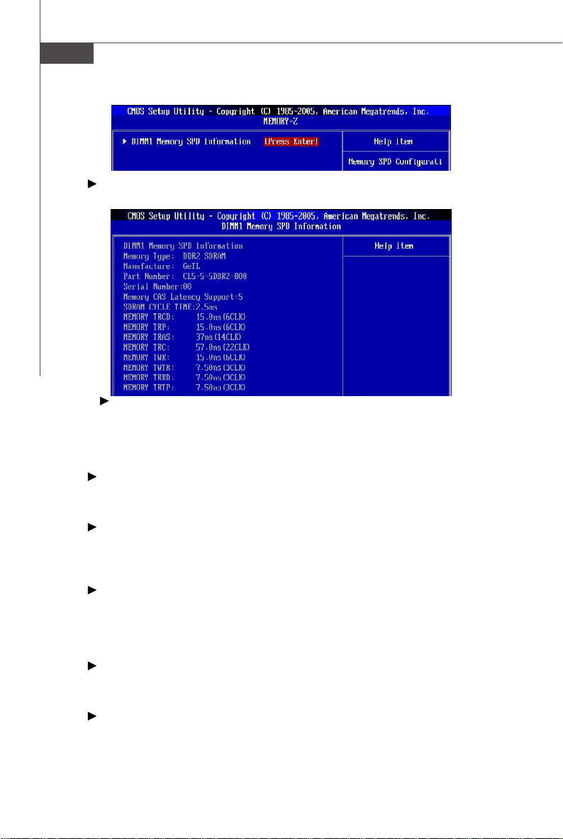
MS-7532 マザーボード
DIMM1 Memory SPD Information
<Enter>キーを押すと、サブメニューが表示されます。
DIMM 1/2/3/4 Memory SPD Information
この項目は現在DIMMメモリ速度情報の状態を表示します。(例えば、メモリのタ
イプ、バンド幅の最大値、製作、部品番号、シリアル番号、SDRAM周期、TCL、
TRCD、TRP、TRAS、TRFC、TWR、TWTR、TRRD及びTRTP)。読取専 用で
す。
CAS Latency (tCL)
SDRAMが読み込みコマンドを受信した後読み込みを開始するまでのタイミング遅延
であるCASレイテンシーを設定します。
tRCD
DRAMを更新すると、行も列も別々にアドレスされます。この項目でRASからCASま
での転送タイミングを決定します。一般的にクロックサイクルの値が小さいほど
DRAMの動作速度が上がります。
tRP
DRAMがリフレッシュに必要とする電荷を蓄積する時間を手動で設定します。RAS信号
のクロック数がこの時間を規定しますが、電荷を蓄積するための時間が足りない場合は
DRAMのリフレッシュは不完全になり、DRAMがデータを保持できなくなることがあり
ます。システムに同期DRAMをインストールした場合のみこの項目が利用 できます。
tRAS
この設定はRASがメモリセルから読み込む及びメモリセルへ書き込むことに掛ける時間
を決定します。
Advance Memory Setting
[Auto]に設定すると、[Advance memory timing]は自 動的にBIOSに決定されます。
Jp-24

FSB/DRAM Ratio
メモリ/FSB倍率の調整を行います。
Adjusted DRAM Frequency (MHz)
調整されたDRAM周波数を表示します。読取専用です。
Adjust PCI Frequency
PCI周波数を選択します。(MHz)
Auto Disable DRAM/PCI Frequency
[Enabled]に設定すると、システムは使用していないPCIスロットのクロック発信を切り、
EMIの発 生を 軽減 する働きがあります。
CPU Voltage / CPU GTL REF0 / CPU GTL REF1 / DRAM Voltage (V)/
DDR_VREF_CA/DA_A/B /MCH Voltage (V)/ MCH GTL REF / VTT FSB Voltage / ICH
Voltage(V)
メモリ、FSBやチップセットの電源状態を調整します。
Spread Spectrum
コンピューターはクロック信号と呼ばれるパルス信号を元に動作しています。クロックジェ
ネレーターがパルス信号を発生する際に、構造上やむを得ずスパイクノイズと呼ばれる電磁
妨害(EMI) が生じます。基本的にはボード上の配線の取り回しによってノイズを相殺するよ
うに工夫しています。しかし特定環境下において外部にノイズが漏れてしまう場合があり、
そのようなケースではスペクトラム拡散方式で信号の波形を変更することにより、ノイズの
漏れを回避することができます。通常は[Disabled]に設定して使用します。また、オーバー
クロックをかけた状態で使用する場合も[Disabled]に設定してください。本機が発生するス
パイクノイズによって、外部の機器が何らかの影響を受けてしまうといった現象が発生する
場合のみ[Enabled]に設定します。有効に設定するとクロック信号の波形が変更されるた
め、それによってシステムの安定性が損なわれる可能性があります。
日 本 語
注意!
1.EMI に問題がない場合は、システムの安定性と性能を最適化するために[Disabled]
に設定 して おい てください。しかし、EMIに問題がある場合は、[Enabled]に設定
してEMIを軽減 してください。
2.Spread Spectrum値は大きければ大きいほどますますEMIを 軽減し、システムが
不安定になります。当地のEMI規定 を 調べって最適のSpread Spectrum値を設定
してください。
3. オーバークロックを使用している場合は必ず[Disable] にしてください。ちょっと
したジッターであっても一時的にブーストを引き起こすことがあり、それによっ
てオーバークロックされたプロセッサがロックしてしまうことがあるからです。
Jp-25

MS-7532 マザーボード
CPU
とメモリのオーバークロック
[D.O.T Control, Adjust CPU FSB Frequency, FSB/Memory Ratio]で、CPUとメモリを
オーバークロックできます。これらのフィールドに関する説明をご参照ください。
注意!
1.CPU速度= CPU FSB周波数 * CPU内倍率
2. 本製品はオーバークロックを非常にサポートできます。ただし周辺装置とコン
ポーネントが特別の設定をできることを確認してください。製品に損傷を与える
恐れがありますので、製品の規格を超える操作はお勧めしません。
オーバークロックが失敗後、二つの方法でシステムを回復できます。
再起動
1. 電源ボタンを押してシステムを3回も再起動します。電流が他のデバイス
もしくはコンポーネントに影響しないために、10秒以上間隔で再起動して
ください。
2. 4回目の再起動の時、BIOSは前のオーバークロックが無効にして、自動的
にデフォルト設定に戻します。以下のメッセージが表示された場合は、ど
んなキーを押してもシステムを正常に起動できます。
Warning !!! The previous overclocking had failed,
and system will restore its defaults setting,
Press any key to continue.......
CMOSをクリア
- バックパネルにはのクリアCMOSボタンを押してデータをクリアします。
Jp-26

ソフトウェアの情報
本製品にはドライバー/ユーティリティCDが同梱さ れています。OSのインストールが終了し
たら、全てのドライバーのインストールし、セットアップを完了させてください。ユーティ
リティソフトはユーザーのニーズに応じてインストールしてください。ドライバー/ユーティ
リティCDには以下の内容が含まれています。
Driver menu - 使用でき るドライバーを表示します。要望によってドライバーをインストー
Utility menu - サポートのソフトウェアアプリケーションを表示します。
WebSite menu- 必 要なウェブサイトを表示します。
ルし、デバイスを起動します。
注意!
MSIのホームページから最新のドライバーやBIOSを入手することができます。
日 本 語
Jp-27

This page is intentionally left blank.
viii

P45-8D
使用手冊
繁體中文
繁體中文
Tc-1

MS-7532 主機板
主機板規格
支援㆗央處理器
- 支援 LGA 775 架構的 Intel
Dual-Core 及 Celeron® 處理器
- 支援 Intel
®
Yorkfield, Wolfdale, Conroe 系列及其以上等級處理器
®
Core™2 Extreme/ Quad/ Duo, Pentium
®
*(有關更多 CPU 的最新訊息,請至微星科技網站:
http://global.msi.com.tw/index.php?func=cpuform)
支援 FSB
- 1600*(OC)/ 1333/ 1066/ 800 MHz
晶片組
- Intel® Eaglelake P45 北橋晶片
- Intel® ICH10/ ICH10R 南橋晶片
記憶體
- 4 條 DDR3 DIMM 支援 DDR3 **1600(OC)/1333/1066/800 MHz SDRAM
(要支援達 8 GB,請見英特爾官方網站標準)
- DDR2 667/ 800 SDRAM
-或 4 條 DDR2 DIMM 支援 DDR2 **1066(OC)/ 800/ 667 MHz SDRAM (最
高 16 GB)
** (有關更多記憶體的最新訊息,請至微星科技網站:
http://global.msi.com.tw/index.php?func=testreport )
LAN
- Realtek® RTL8111C 支援 PCIE LAN 10/100/1000 高速乙太網路
音效
- 由 Realtek
®
ALC888 晶片整合
- 最多支援 8 聲道智慧型音效輸出
- 與 Azalia 1.0 規格相容
- 支援 Microsoft
®
Vista™ Premium 規格
IDE
®
- JMicron
JMB363 晶片支援 1 個 IDE 連接埠
- 支援 Ultra DMA 66/ 100/ 133 模式
- 支援 PIO, 主控匯流排操作模式
SATA
- ICH10/ ICH10R 晶片支援 6 個 SATA II 連接埠 (SATA1~6)
®
- JMicron
JMB363 晶片支援 2 個 SATA II 連接埠 (SATA7, SATA8)
- 支援資料傳輸率達每秒 3 Gb
RAID
- ICH10R 晶片控制的 SATA 1~6 支援 Intel® Matrix Storage 技術 (AHCI+
RAID 0/ 1/ 5/ 10)
®
- JMicron
JMB363 晶片控制的 SATA 7, SATA8 連接埠支援 RAID 0/ 1
IEEE 1394(選配)
- 由 JMicron
®
JMB381 晶片整合
- 最高支援 2 個連接埠 (背板及板載各一)
Tc-2

軟碟機
- 1 個軟碟機連接埠
- 支援 1 部 360KB、720KB、1.2MB、1.44MB 及 2.88MB 規格的軟碟機
接頭
背板
- 1 個 PS/2 滑鼠連接埠
- 1 個 PS/2 鍵盤連接埠
- 1 個平行埠
- 1 個序列埠
- 1 個清除 CMOS 按鈕
- 4 個 USB 2.0 連接埠
- 1 個 IEEE 1394 連接埠(選配)
- 1 個 LAN 接頭
- 6 個音效接頭
內建接頭
- 4 個 USB 2.0 接頭
- 1 個 IEEE 1394 接頭(選配)
- 1 個機殼警告接頭
- 1 個 S/PDIF-out 接頭
- 1 個 CD-in 接頭
- 1 個前置音效接頭
- 1 個 TPM 接頭(選配)
- 1 個電源按鈕
- 1 個重開機按鈕
- 1 個硬體超頻 FSB 開關
- 1 個序列埠接頭
TPM(選配)
- 支援 TPM
插槽
- 1 個 PCI Express x16 插槽,支援 PCI Express 2.0 速度
- 1 個 PCI Express x1 插槽
- 3 個 PCI 插槽
尺寸
- ATX 規格 (30.5 公分 x 24.4 公分)
裝機孔
- 9 個裝機孔
繁體中文
Tc-3

MS-7532 主機板
RESET
OC_SW1, p.Tc-15
SYSFAN1, p.Tc-10
PCI Express Slot,
p.Tc-15
滑鼠/鍵盤,
p.Tc-16
JPWR2,
p.Tc-14
序列埠,
p.Tc-16
ON
123
平行埠,
p.Tc-16
CPU,
p.Tc-5
清除CMOS
按鈕, p. Tc-16
IEEE 1394 埠,
p.Tc-17
USB 埠,
p.Tc-17
DDR2,
p.Tc-7
LAN,
p.Tc-17
音效輸入
音效輸出
麥克風
CPUFAN1,
p.Tc-10
RS-輸出
CS-輸出
SS-輸出
音效埠,
p.Tc-17
DDR3, p.Tc-7
SYSFAN2, p.Tc-10
JPWR1, p.Tc-14
IDE1, p.Tc-10
JCI1, p.Tc-13
SATA1~8, p.Tc-11
PCI Slot, p.Tc-15
JAUD1,
p.Tc-12
JCD1,
p.Tc-13
SPDIF1,
p.Tc-12
FDD1,
p.Tc-10
J1394_1,
p.Tc-11
JCOM1,
p.Tc-13
JTPM1,
p.Tc-13
JUSB1~4, p.Tc-12
RESET1/POWER1, p.
Tc-14
JFP2/1, p.Tc-11
P45-8D 系列(MS-7532 v1.X) 主機板
快速元件指南
Tc-4

㆗央處理器
主機板使用 LGA775 架構的 CPU 插座,在安裝 CPU 時,請確認附㈲散熱風扇以避免 CPU 過熱。
若無散熱風扇,請向經銷商洽購。並在開機前,先將風扇正確地安裝在主機板上。
有關更多 CPU 的最新訊息,請至微星科技網站:
http://global.msi.com.tw/index.php?func=cpuform
㊟意事㊠
溫度過高
溫度過高,會嚴重損壞 CPU 以及系統。請確保散熱風扇正常運作,避免 CPU 過熱。請
於 CPU 與散熱器間均勻塗抹散熱膏或貼上耐溫膠帶,以加強散熱。
更換CPU
更換 CPU 時,應先關掉 ATX 電源開關,或拔掉電源線,以免損壞 CPU。
超頻使用
即使本主機板設計為可超頻運作,但在將其調整為超頻運作時,請確認系統零組件可承
受此非正常的設定。任何在非本產品規格建議下的操作,我們不保證其造成的損壞
及操作時的風險。
繁體中文
Tc-5
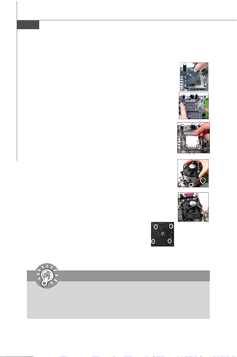
MS-7532 主機板
安裝 LGA775 架構的㆗央處理器與散熱風扇
1. CPU 插座上面有塑膠保護蓋以免 CPU 插座受損。安裝 CPU 前,請勿取下。
2. 由插座側邊將保護蓋取下(如箭頭所示)。
3. 插座針腳露出。
4. 開啟拉桿。
5. 將拉桿拉起,打開固定蓋。
6. 確認 CPU 正確安裝方向,將其置入插座中。以手指抓住處理器邊緣推入
插座。注意對準對齊點。
7. 檢視 CPU 是否已安裝好。若未安裝好,請垂直拿出 CPU 重新安裝。
8. 蓋上固定蓋。
9. 輕壓下拉桿,然後將拉桿固定於固定蓋旁的勾槽。
10. 對齊風扇和主機板上的安裝孔。將風扇用力往下壓,直到四個卡榫,卡進主
機板的四個孔裡。
11.壓下四個卡榫固定風扇。旋轉卡榫鎖好(請參考卡榫上標示的正確方向)。
12.檢查主機板背面,確認四個卡榫已正確插入。
㊟意事㊠
1. 請於第三章 BIOS 中監測 CPU 溫度。
2. 未安裝 CPU 時,請使用塑膠保護蓋保護 CPU 針腳。
3. 本節主機板圖示僅作安裝中央處理器及散熱風扇示範用。該圖示可能會與您購置的主機
板外觀有所差異。
對齊點
Tc-6
 Loading...