

Page 1
i
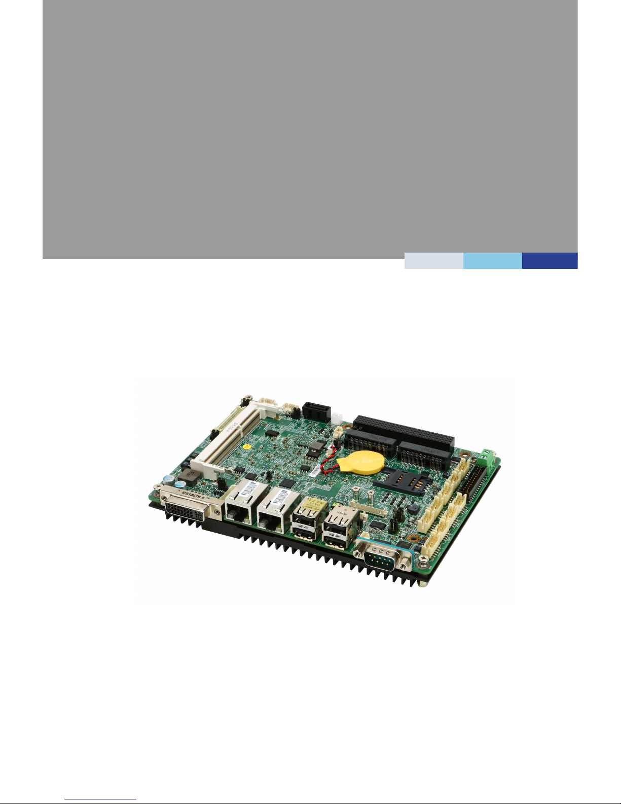
MS-98D1
(v1.x) Industrial Computer Board
Page 2

ii
Preface MS-98D1
Copyright Notice
The material in this document is the intellectual property of MICRO-STAR INTERNATIONAL. We take every care in the preparation of this document, but no guarantee is given as to the correctness of its contents. Our products are under continual improvement and we reserve the right to make changes without notice.
Trademarks
All trademarks are the properties of their respective owners.
Revision History
Revision Date
V1.1 2014/06
Technical Support
If a problem arises with your system and no solution can be obtained from the
user’s manual, please contact your place of purchase or local distributor. Alterna
-
tively, please try the following help resources for further guidance.
Visit the MSI website for technical guide, BIOS updates, driver updates and other
information, or contact our technical sta via
http://support.msi.com/
Page 3

iii
Safety Instructions
Always read the safety instructions carefully.
Keep this User’s Manual for future reference.
Keep this equipment away from humidity.
Lay this equipment on a reliable flat surface before setting it up.
The openings on the enclosure are for air convection hence protects the
equipment from overheating. DO NOT COVER THE OPENINGS.
Make sure the voltage of the power source and adjust properly before
connecting the equipment to the power inlet.
Place the power cord such a way that people can not step on it. Do not place
anything over the power cord.
Always Unplug the Power Cord before inserting any add-on card or mod
-
ule.
All cautions and warnings on the equipment should be noted.
Never pour any liquid into the opening that could damage or cause electrical
shock.
If any of the following situations arises, get the equipment checked by
service personnel:
The power cord or plug is damaged.
Liquid has penetrated into the equipment.
The equipment has been exposed to moisture.
The equipment does not work well or you can not get it work according
to User’s Manual.
The equipment has dropped and damaged.
The equipment has obvious sign of breakage.
DO NOT LEAVE THIS EQUIPMENT IN AN ENVIRONMENT
UNCONDITIONED, STORAGE TEMPERATURE ABOVE 60oC (140oF), IT
MAY DAMAGE THE EQUIPMENT.
警告使用者:
這是甲類資訊產品,在居住的環境中使用時,可能會造成無線電干擾,在這種情
況下,使用者會被要求採取某些適當的對策。
■
■
■
■
■
■
■
■
■
■
■
◯
◯
◯
◯
◯
◯
■
Page 4
iv
Preface MS-98D1
Chemical Substances Information
In compliance with chemical substances regulations, such as the EU REACH
Regulation (Regulation EC No. 1907/2006 of the European Parliament and the
Council), MSI provides the information of chemical substances in products at:
http://www.msi.com/html/popup/csr/evmtprtt_pcm.html
Battery Information
European Union:
Batteries, battery packs, and accumulators should not be
disposed of as unsorted household waste. Please use the
public collection system to return, recycle, or treat them in
compliance with the local regulations.
Taiwan:
For better environmental protection, waste batteries should
be collected separately for recycling or special disposal.
California, USA:
The button cell battery may contain perchlorate material and requires special
handling when recycled or disposed of in California.
For further information please visit:
http://www.dtsc.ca.gov/hazardouswaste/perchlorate/
Danger of explosion if battery is incorrectly replaced. Replace only with the
same or equivalent type recommended by the manufacturer.
Page 5
v
CE Conformity
Hereby, Micro-Star International CO., LTD declares that this device
is in compliance with the essential safety requirements and other
relevant provisions set out in the European Directive.
FCC-A Radio Frequency
Interference Statement
This equipment has been tested and found to comply with the
limits for a Class A digital device, pursuant to Part 15 of the FCC Rules. These
limits are designed to provide reasonable protection against harmful interference
when the equipment is operated in a commercial environment. This equipment
generates, uses and can radiate radio frequency energy and, if not installed and
used in accordance with the instruction manual, may cause harmful interference
to radio communications. Operation of this equipment in a residential area is
likely to cause harmful interference, in which case the user will be required to
correct the interference at his own expense.
Notice 1
The changes or modifications not expressly approved by the party responsible for
compliance could void the user’s authority to operate the equipment.
Notice 2
Shielded interface cables and AC power cord, if any, must be used in order to
comply with the emission limits.
VOIR LA NOTICE D’INSTALLATION AVANT DE RACCORDER AU RESEAU.
This device complies with Part 15 of the FCC Rules. Operation is subject to the
following two conditions:
this device may not cause harmful interference, and
this device must accept any interference received, including interference that
may cause undesired operation.
WEEE Statement
Under the European Union (“EU”) Directive on Waste Electrical and
Electronic Equipment, Directive 2002/96/EC, which takes effect on
August 13, 2005, products of “electrical and electronic equipment”
cannot be discarded as municipal waste anymore and manufacturers
of covered electronic equipment will be obligated to take back such products at
the end of their useful life. MSI will comply with the product take back requirements at the end of life of MSI-branded products that are sold into the EU. You
can return these products to local collection points.
1)
2)
Page 6

vi
Preface MS-98D1
Contents
Copyright Notice ............................................................................................ ii
Trademarks ................................................................................................... ii
Revision History
............................................................................................ ii
Technical Support
.......................................................................................... ii
Safety Instructions
.........................................................................................iii
Chemical Substances Information
............................................................... iv
Battery Information
....................................................................................... iv
CE Conformity
............................................................................................... v
FCC-A Radio Frequency Interference Statement
......................................... v
WEEE Statement .......................................................................................... v
1. Overview.......................................................................................1-1
Mainboard Specifications ...........................................................................1-2
Mainboard Layout
......................................................................................1-4
2. Hardware Setup ...........................................................................2-1
Quick Component Guide ............................................................................ 2-2
Memory ...................................................................................................... 2-3
Power Supply .............................................................................................2-4
Rear Panel I/O ...........................................................................................2-5
Connector ...................................................................................................2-7
Jumper ..................................................................................................... 2-14
Slot ...........................................................................................................2-17
3. BIOS Setup ...................................................................................3-1
Entering Setup ...........................................................................................3-2
The Menu Bar ............................................................................................3-4
Main
...........................................................................................................3-5
Advanced ................................................................................................... 3-6
Boot .......................................................................................................... 3-11
Security
.................................................................................................... 3-12
Chipset
.....................................................................................................3-14
Power .......................................................................................................3-15
Save & Exit
...............................................................................................3-17
A. WDT & GPIO ............................................................................... A-1
WDT Sample Code ................................................................................... A-2
GPIO Sample Code .................................................................................. A-3
Page 7

1-1-1
Thank you for choosing the MS-98D1, an excellent industrial computer
board.
Based on the innovative Intel
®
NM10 chipset for optimal system efficiency, the MS-98D1 accommodates the Intel® Cedarview-M/ Cedarview-D
processor and supports 1 DDR3 800/1066 SO-DIMM slot to provide the
maximum of 2GB/ 4GB memory capacity.
The MS-98D1 is durable under extreme environments and suitable to be
applied in every industrial field, such as digital signage, kiosk, gaming,
industrial control automation and POS.
1 Overview
Page 8

1-2
Overview MS-98D1
Mainboard Specications
Processor
Intel® Atom D2550/ 1.86GHz, N2800/1.86GHz, N2600/1.6GHz■
Chipset
Intel® NM10 chipset ■
Memory
1 DDR3 800/ 1066MHz Unbuffered, non-ECC SO-DIMM slot, supporting
the maximum of 4GB (N2600 only supports DDR3 800 MHz with the maximum of 2GB)
■
LAN
LAN1: Intel® I210-AT GbE LAN
LAN1: Intel® I210-AT GbE LAN
■
■
Audio
Realtek ALC887 audio codec
Compliant with Azalia 1.0 specs
■
■
Storage
1 SATA 3Gb/s port (SATA1)
1 mSATA function included with Mini-PCIe slot
■
■
Graphics
Graphics integrated in Intel processor■
Rear Panel I/O
1 DVI-I port
2 Gigabit LAN jacks
4 USB 2.0 ports
1 RS-232/422/485 serial port
■
■
■
■
Page 9

1-3
Onboard Pinheaders/ Connectors/ Jumpers
1 Dual USB 2.0 wafer connector
5 Serial port connectors
1 Parallel port connector
1 Front panel connector
1 PS/2 keyboard/ mouse combo connector
2 LVDS connectors
2 LVDS power jumpers
1 GPIO connector
1 Audio connector
1 Amplifier connector
1 System fan connector
1 SATA power connector
1 Clear CMOS jumper
2 Serial port power jumpers
1 AT/ATX select jumper
1 PCI-104 power jumper
2 Inverter connectors
2 Inverter power jumpers
1 SIM Card Holder
2 NVM LAN jumpers
■
■
■
■
■
■
■
■
■
■
■
■
■
■
■
■
■
■
■
■
Slot
2 Mini-PCIe slot (including 1 x mSATA function)
1 PCI-104 slot
■
■
Form Factor
165mm x 115mm (EPIC-size)■
Environmental
Operating Temperature: 0oC ~ 60oC
Storage Temperature: -20oC ~ 80oC
Humidity: 10% ~ 90% RH, Non-Condensing
Power input DC 9~36V
■
■
■
■
Page 10
1-4
Overview MS-98D1
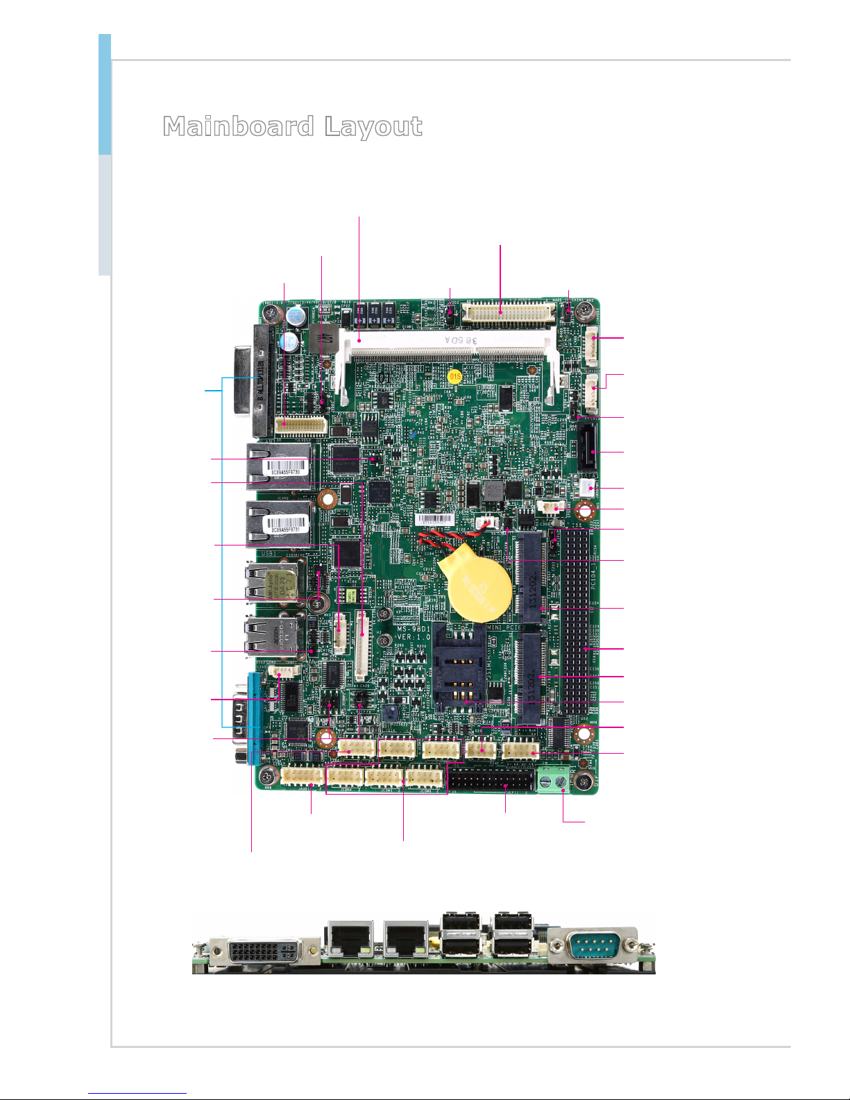
Mainboard Layout
Serial PortLAN
Port
USB 2.0
Port
LAN
Port
DVI-I Port
Back Panel
Front Panel
Connector
Fan Connector
SIM Card Holder
COM Port
Jumper
Clear CMOS
Jumper
AT/ATX
Jumper
SO-DIMM Slot
PCI104 Power
Connector
COM Port
Connector
USB 2.0 Connector
SATA Port
Parallel Port
Connector
Amplier
Connector
LVDS2 Inverter
Power Jumper
HDD Power
Connector
PCI-104 Slot
GPIO Connector
Port 80
Connector
PS/2
Keyboard
/ Mouse
Combo
Connector
LVDS1 Connector
LVDS1 Power Jumper
LVDS2 Power Jumper
LVDS2 Inverter
Connector
LVDS2 Connector
LVDS1
Inverter
Power Jumper
Mini-PCIe Slot
Mini-PCIe Slot
Audio
Connector
LVDS1 Inverter
Connector
NVM LAN1
Jumper
NVM LAN2
Jumper
DC-In
Connector
Page 11

2-2-1
This chapter provides you with the information about hardware setup
procedures. While doing the installation, be careful in holding the com
ponents and follow the installation procedures. For some components, if
you install in the wrong orientation, the components will not work properly.
Use a grounded wrist strap before handling computer components. Static
electricity may damage the components.
2 Hardware Setup
Page 12
2-2
Hardware Setup MS-98D1
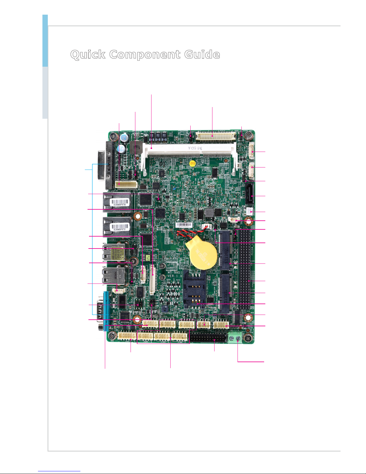
Quick Component Guide
Back Panel,
p. 2-5
JFP1, p. 2-8
SYSFAN1, p. 2-7
JSIM1, p. 2-17
JCOMP2,
p. 2-15
JBAT1, p. 2-14
JAT1,
p. 2-14
DIMM1, p. 2-3
JPCIP1, p. 2-16
JCOM3, JCOM2
JCOM4, JCOM5, JCOM6, p. 2-8
JUSB1, p. 2-9
SATA1, p. 2-7
JLPT1, p. 2-11
JAMP1,
p. 2-8
JINV2, p. 2-16
JHDDPWR1,
p. 2-4
PC104_1, p. 2-18
J1, p. 2-8
JDP1, p. 2-11
JKBMS1,
p. 2-10
JLVDS1, p. 2-12
JVDD1, , p. 2-15
JVDD2, p. 2-15
JINVDD1,
p. 2-12
JLVDS2, p. 2-13
JINV1,
p. 2-16
MINI_PCIE2, p. 2-17
JAUD1, p. 2-9
JCOMP1,
p. 2-15
MINI_PCIE1,
p. 2-17
JINVDD2,
p. 2-13
JNVM1, p. 2-16
JNVM2, p. 2-16
JPWR1, p. 2-7
Page 13
2-3
Memory
These DIMM slots are intended for memory modules.
Installing Memory Modules
Locate the SO-DIMM slot. Align the notch on the DIMM with the key on the
slot and insert the DIMM into the slot.
Push the DIMM gently downwards until the slot levers click and lock the
DIMM in place.
To uninstall the DIMM, ip the slot levers outwards and the DIMM will be
released instantly
Important
You can barely see the golden nger if the DIMM is properly inserted in the DIMM
slot.
1.
2.
3.
Page 14

2-4
Hardware Setup MS-98D1
Power Supply
HDD Power Connector: JHDDPWR1
This connector is used to provide power for hard disk drives.
1
.G N
D
2. VCC 5
Important
Make sure that all power connectors are connected to the power supply to ensure
stable operation of the motherboard.
Page 15
2-5
Rear Panel I/O
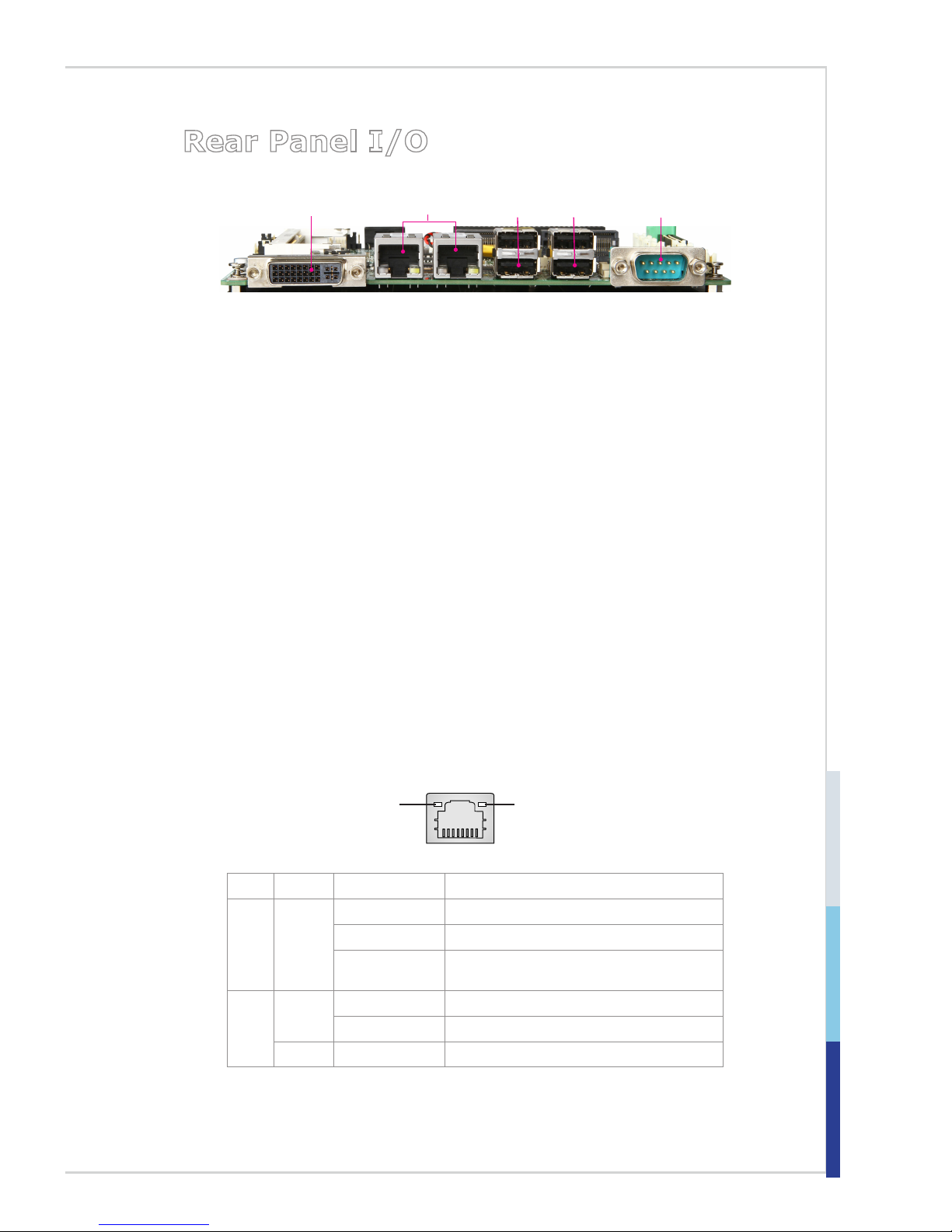
Serial Port
LAN
Ports
USB 2.0
Ports
DVI-I Port
USB 2.0
Ports
DVI-I Port
The DVI-I (Digital Visual Interface-Integrated) connector allows you to connect an
LCD monitor. It provides a high-speed digital interconnection between the computer and its display device. To connect an LCD monitor, simply plug your monitor cable into the DVI connector, and make sure that the other end of the cable
is properly connected to your monitor (refer to your monitor manual for more
information.)The DVI-I (Digital Visual Interface-Integrated) connector allows you
to connect an LCD monitor. It provides a high-speed digital interconnection between the computer and its display device. To connect an LCD monitor, simply
plug your monitor cable into the DVI connector, and make sure that the other end
of the cable is properly connected to your monitor (refer to your monitor manual
for more information.)
USB 2.0 Port
The USB (Universal Serial Bus) port is for attaching USB devices such as
keyboard, mouse, or other USB-compatible devices..
LAN Jack
The standard RJ-45 LAN jack is for connection to the Local Area Network (LAN).
You can connect a network cable to it.
Yellow Green/ Orange
LED Color LED State Condition
Left Yellow Off LAN link is not established.
On (steady state) LAN link is established.
On (blinking) The computer is communicating with another
computer on the LAN.
Right
Green Off 10 Mbit/sec data rate is selected.
On 100 Mbit/sec data rate is selected.
Orange On 1000 Mbit/sec data rate is selected.
Page 16

2-6
Hardware Setup MS-98D1
RS-232/422/485 Serial Port
The serial port is a 16550A high speed communications port that sends/ receives
16 bytes FIFOs. You can attach a serial mouse or other serial devices directly to
the connector.
PIN SIGNAL DESCRIPTION
1
2
3
4
5
6
7
8
9
DCD
RXD
TXD
DTR
GND
DSR
RTS
CTS
VCC_COM1
Data Carrier Detect
Receive Data
Transmit Data
Data Terminal Ready
Signal Ground
Data Set Ready
Request To Send
Clear To Send
Voltage select setting by jumper
RS-232
PIN SIGNAL DESCRIPTION
1
2
3
4
5
6
7
8
9
422 TXD422 RXD+
422 TXD+
422 RXDGND
NC
NC
NC
NC
Transmit Data, Negative
Receive Data, Positive
Transmit Data, Positive
Receive Data, Negative
Signal Ground
No Connection
No Connection
No Connection
No Connection
RS-422
PIN SIGNAL DESCRIPTION
1
2
3
4
5
6
7
8
9
485 TXDNC
485 TXD+
NC
GND
NC
NC
NC
NC
Transmit Data, Negative
No Connection
Transmit Data, Positive
No Connection
Signal Ground
No Connection
No Connection
No Connection
No Connection
RS-485
Page 17
2-7
Connector
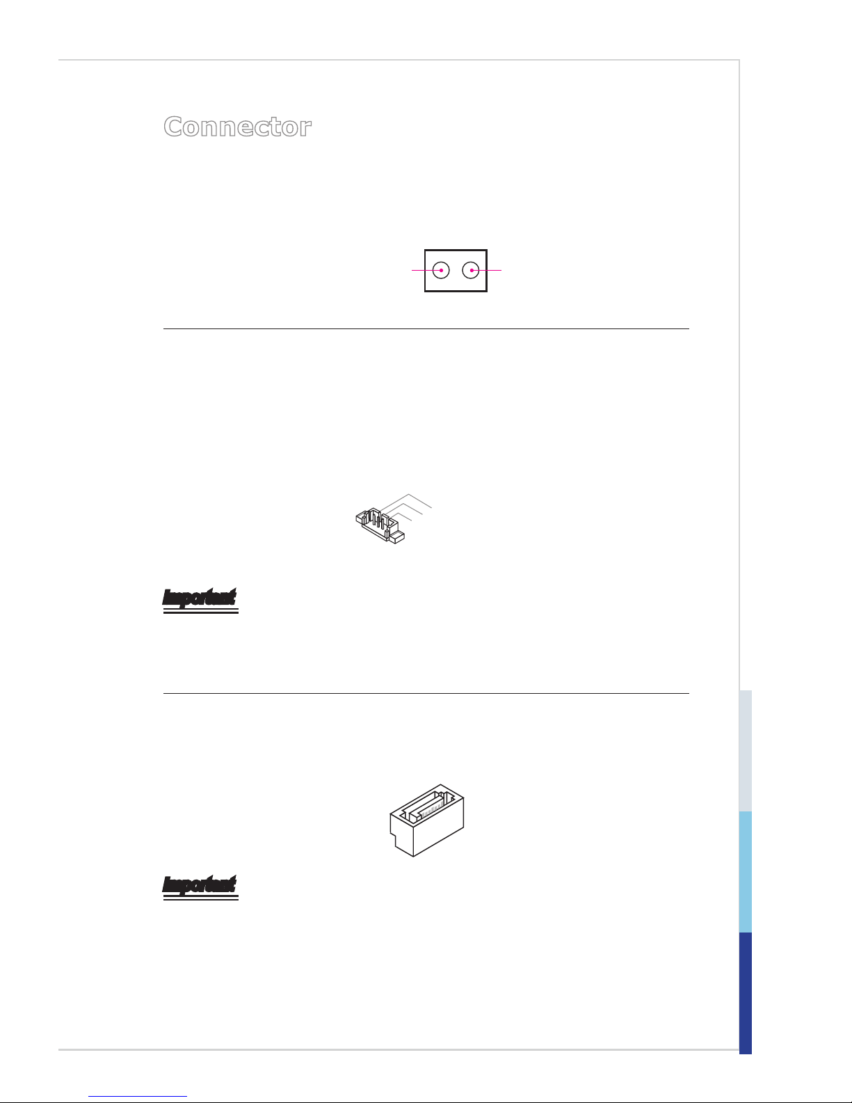
DC Power Connector: JPWR1
Thi s connector i s used to provi de power to the motherboard.
21
DC-In (9~36V)
GND
Fan Power Connector: SYSFAN1
The fan power connectors support system cooling fan with +12V. When connecting the wire to the connectors, always note that the red wire is the positive
and should be connected to the +12V; the black wire is Ground and should be
connected to GND. If the motherboard has a System Hardware Monitor chipset
onboard, you must use a specially designed fan with speed sensor to take advantage of the system fan control.
2. + 12V
3. S ens o r
1
.G r oun d
Important
Please refer to the recommended CPU fans at processor’s official website or
consult the vendors for proper CPU cooling fan.
Fan cooler sets with 3- or 4-pin power connector are both available.
Serial ATA Connector: SATA1
This connector is a high-speed Serial ATA interface port. Each connector can
connect to one Serial ATA device.
Important
Please do not fold the SATA cable into a 90-degree angle. Otherwise, data loss
may occur during transmission.
•
•
Page 18
2-8
Hardware Setup MS-98D1
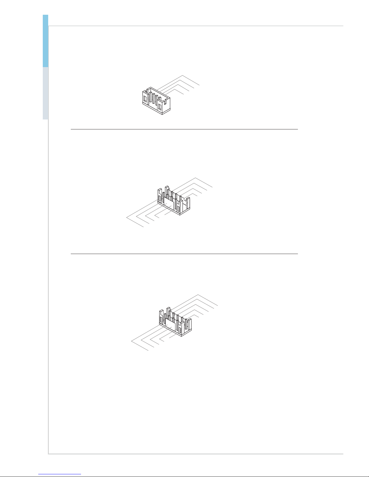
Audio Amplifier Connector: JAMP1
The JAMP1 is used to connect audio amplifiers to enhance audio performance.
1.AMP_ L-
2.AMP_ L+
3.AMP_ R-
4.AMP_
R
+
Front Panel Connector: JFP1
This front panel connector is provided for electrical connection to the front panel
switches & LEDs and is compliant with Intel Front Panel I/O Connectivity Design
Guide.
8
.GN
D
3.HD_ LE
D
1.HDD +
6
.FP_P SI
N
5
.GN
D
4.SUS _LE
D
7
.FP_R ST#
2.PWR _LE
D
9.NC
GPIO Connector: J1
This connector is provided for the General-Purpose Input/Output (GPIO)
peripheral module.
9.N_G PO
0
8.N_G PI
1
3.N_G PO
3
1
.GN
D
6.N_G PI
2
5.N_G PO
2
4.N_G PI
3
7.N_G PO
1
2.5VS B
10.N_ GPI
0
Page 19
2-9
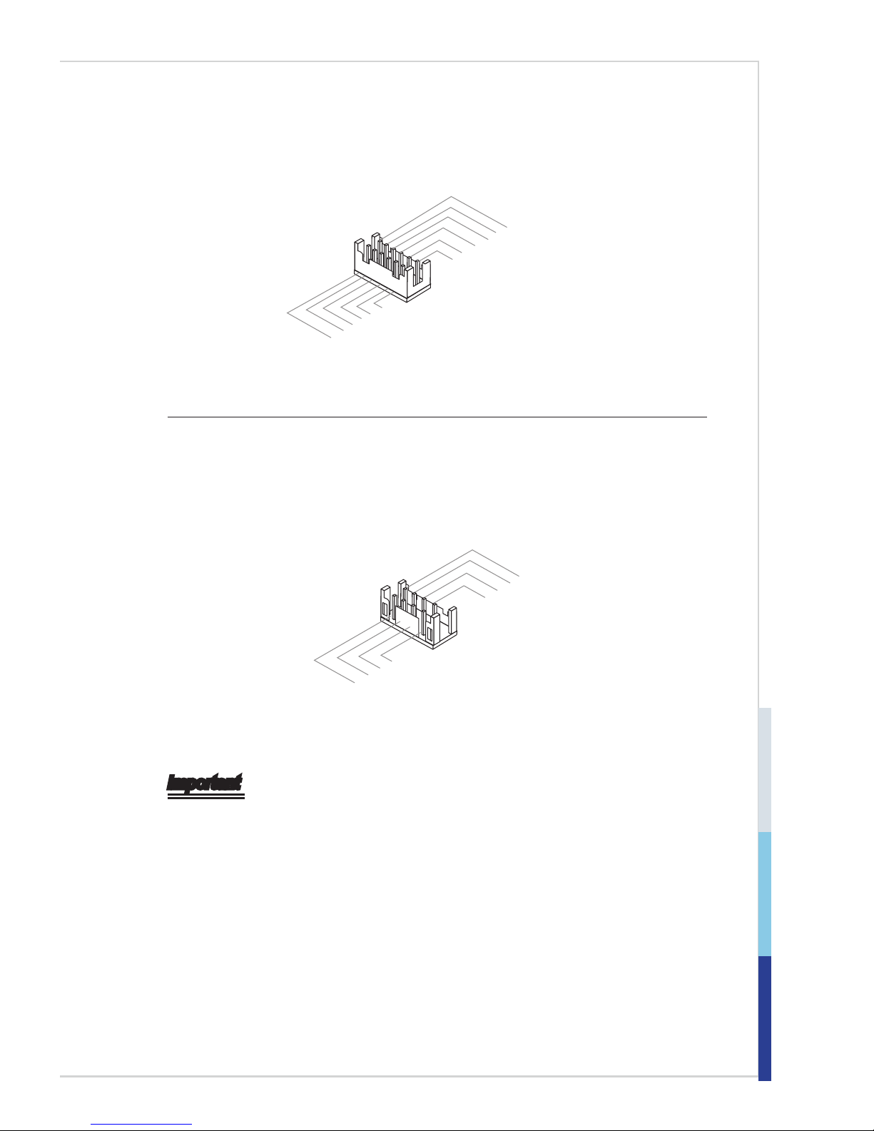
Audio Connector: JAUD1
This connector allows you to connect the additional audio panel.
1.LIN E1_1 R_J
8.LIN E1_J
D
10.GN
D
3.LIN E1_1 L_J
6.MIC 1_J
D
5.LIN E_FO UTR_ J
4.MIC 1_L_ J
7.LIN E_FO UTL_ J
2.MIC 1_R_ J
12.GN
D
9
.FRON T_JD
11
.GN
D
Front USB 2.0 Connector: JUSB1
The USB connector is ideal for connecting high-speed USB interface peripherals
such as USB HDD, digital cameras, MP3 players, printers, modems
and the like.
8. SVC C 3
3. SBD 5 -
1. SVC C 3
6. SBD 4 -
5. SBD 5 +
4. SBD 4
+
7
.G N
D
2
.G N
D
Important
Note that the pins of VCC and GND must be connected correctly to avoid possible
damage.
Page 20
2-10
Hardware Setup MS-98D1
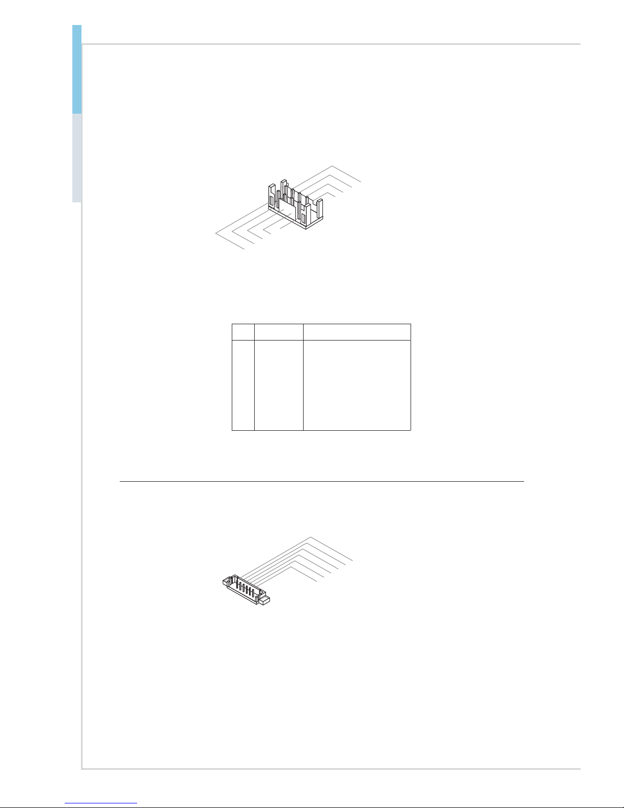
Serial Port Connector: COM2~6
This connector is a 16550A high speed communications port that sends/ receives
16 bytes FIFOs. You can attach serial devices to it through the optional serial port
bracket.
8.COM _NCT S2~6
3.COM _NTD 2~
6
1.COM _NDC D2~
6
6.COM _NDS R2~
6
5
.GN
D
4.COM _NDT R2~
6
7.COM _NR
TS2~
6
2.COM _NRD 2~
6
9.VCC _COM 2&VC C_CO M3
PIN SIGNAL DESCRIPTION
1
2
3
4
5
6
7
8
9
DCD
RD
TD
DTR
GND
DSR
RTS
CTS
VCC_COM
Data Carrier Detect
Receive Data
Transmit Data
Data Terminal Ready
Signal Ground
Data Set Ready
Request To Send
Clear To Send
Voltage select setting by jumper
RS-232
PS/2 Keyboard / Mouse Combo Connector: JKBMS1
The PS/2® mouse/ keyboard connector is for a PS/2® mouse/keyboard.
6.MS
CLK_PH#
4.KBCLK_PH #
2.Ground
5.VCC5
3.MSD
A
T_PH
#
1.KBD
AT
_P
H
#
Page 21
2-11
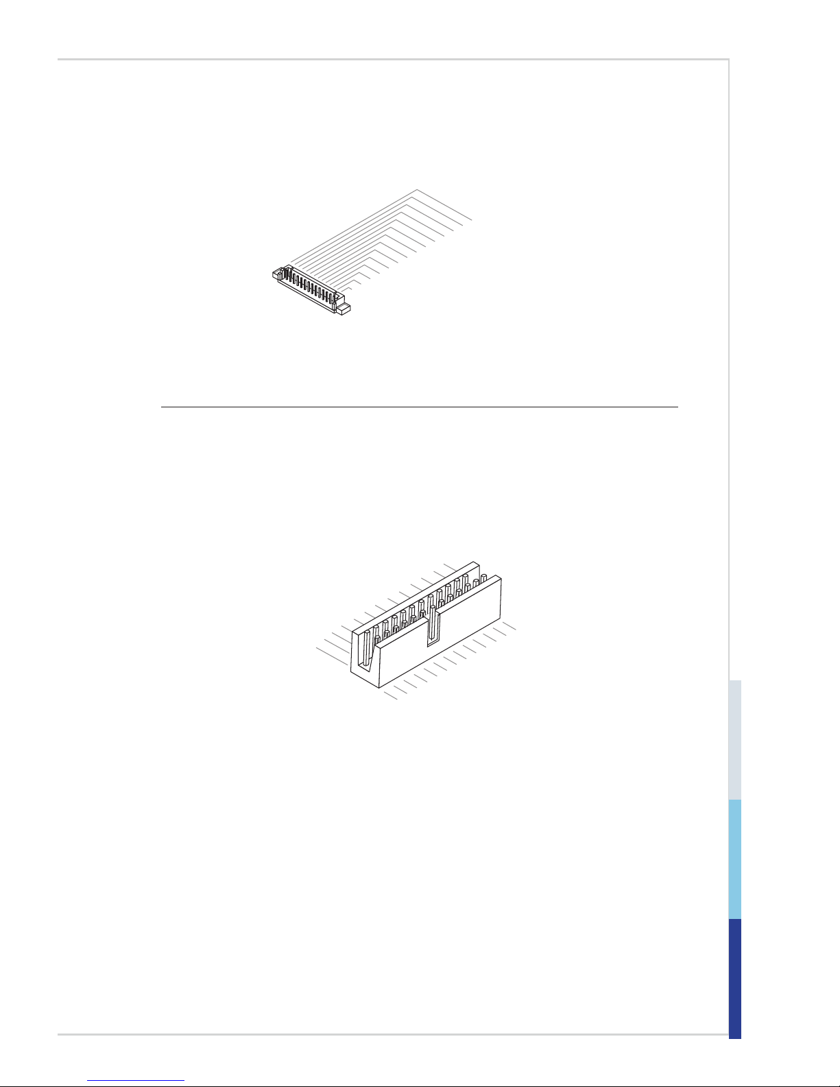
Port 80 Connector: JDP1
This pinheader is intended for Transport Control Protocol (TCP) port 80.
2.LPC _AD3
5.LPC _AD0
10.VC C5
8.SER IRQ
13.N/
A
3.LPC _AD2
6.L_L DRQ0 #
11
.VCC3
9
.TPM_ PL
TRST
#
14.GN
D
1.LPC _FRA ME
#
4.LPC _AD1
7.LPC _DEB UG_C LK
12.GN
D
Parallel Port Connector: JLPT1
The mainboard provides a 26-pin header for connection to an optional parallel
port bracket. The parallel port is a standard printer port that supports Enhanced
Parallel Port (EPP) and Extended Capabilities Parallel Port (ECP) mode.
1.RST B
#
3.PRN D0
5.PRN D1
7.PRN D2
9.PRN D3
11
.PRND 4
13.PR ND5
15.PR ND6
17.PR ND7
19.AC K#
21.BU SY
23.PE
25.SL CT
10.Gr ound
14.Gr ound
8.LPT _SLIN
#
12.Gr ound
6.PIN IT#
4.ERR #
2.AFD #
24.Gr ound
22.Gr ound
26.No
Pin
20.Gr ound
18.Gr ound
16.Gr ound
Page 22
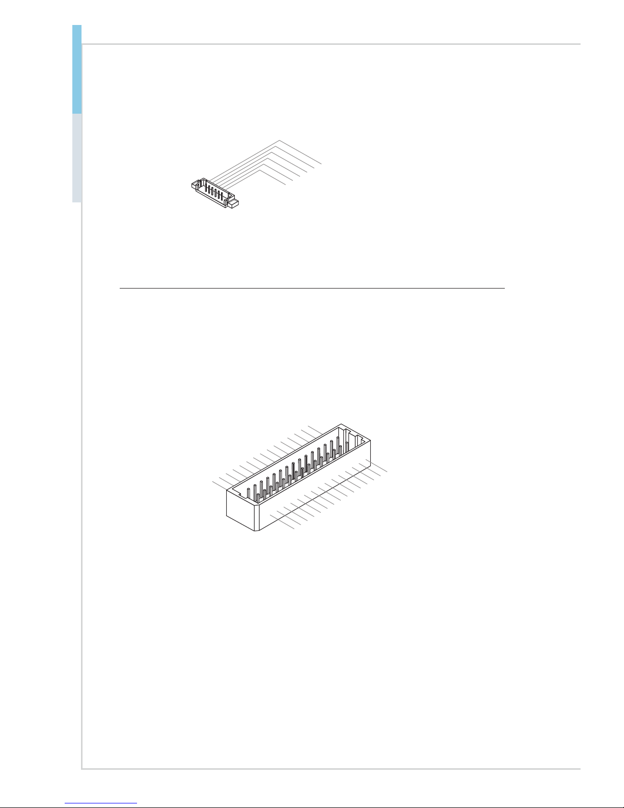
2-12
Hardware Setup MS-98D1
LVDS Inverter Connector: JINVDD1
The connector is provided for LCD backlight options.
6
.Ground
4.L_BKL
TCTL(SIO_BKL
TCTL
)
2.
INV_VDD(5V /12V
D
C)
5
.Ground
3.JINV_ON( CPU_ BKL
TEN)
1
.INV_VDD(5 V/12 V
D
C)
LVDS Connector: JLVDS1
The LVDS (Low Voltage Differential Signal) connector provides a digital interface
typically used with flat panels. After connecting an LVDS interface flat panel to
the JLVDS1, be sure to check the panel datasheet and set the LVDS jumper to
proper power voltage.
1.+12 V
3.+12 V
5.CPU _BKL
TEN
7.L_B KL
TCTL
9.N/
A
11
.GN
D
13.GN
D
15.GN
D
17.
LV
DS_VD D
19.
LV
DS_VD D
21.VC C3
23.GN
D
25.
LV
DS_DD C_DA
TA
27.
LV
DS_DD C_CL K
29.GN
D
6
.GN
D
8.LCD 1CLK
10.LC D1CL K
#
12.GN
D
14.LC D1DO
2
18.GN
D
20.LC D1DO
1
22.LC D1DO 1#
26.LC D1DO
0
24.GN
D
28.LC D1DO 0#
30.GN
D
16.LC D1DO 2#
2.LCD 1DO
3
4.LCD 1DO3 #
Page 23
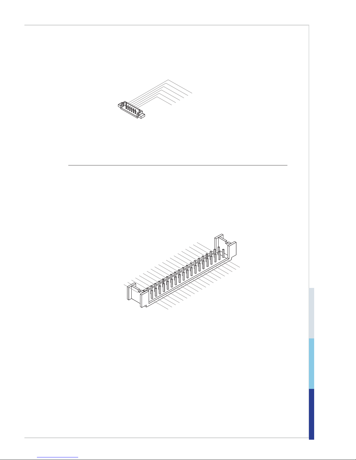
2-13
LVDS Inverter Connector: JINVDD2
The connector is provided for LCD backlight options.
6.Ground
4.L_BKL
T
_CTRL
#
2.
J
INV_VDD(5V /12V
DC
)
5.Ground
3
.INV_O
N
1.JINV_VDD (5V/ 12
V
DC
)
LVDS Connector: JLVDS2
The LVDS (Low Voltage Differential Signal) connector provides a digital interface
typically used with flat panels. After connecting an LVDS interface flat panel to
the JLVDS1, be sure to check the panel datasheet and set the LVDS jumper to
proper power voltage.
39.
LV
D
SB_CL K
#
27.
LV
D
SB_DA
TA
#1
25.
LV
D
SB_DA
TA
1
23.GN
D
21.
LV
D
SA_DA
TA
#3
19.
LV
D
SA_DA
TA
3
17.GN
D
15.
LV
D
SA_DA
TA
#1
13.
LV
D
SA_DA
TA
1
11
.LBKL
T_EN_ C
9.L_B KL
T_CTR L
#
7.DDC _CLK
5.LCD _VDD
3.VCC 3
1.+12 V
40.
LV
D
SA_CL K
#
28.
LV
D
SB_DATA
#0
26.
LV
D
SB_DA
TA
0
24.GN
D
22.
LV
D
SA_DA
TA
#2
20.
LV
D
SA_DA
TA
2
18.GN
D
16.
LV
D
SA_DA
TA
#0
14.
LV
D
SA_DA
TA
0
12.GN
D
1
0.
LV
DS_VD D_E
N
8.DDC _DA
TA
6.LCD _VDD
4.+12 V
2.+12 V
37.
LV
DSB_C LK
35.GN
D
33.
LV
D
SB_DA
TA
#3
31.
LV
D
SB_DA
TA
3
29.GN
D
38.
LV
D
SA_CL K
36.GN
D
34.
LV
D
SB_DA
TA
#2
32.
LV
D
SB_DA
TA
2
30.GN
D
Page 24
2-14
Hardware Setup MS-98D1
Jumper
Important
Avoid adjusting jumpers when the system is on; it will damage the motherboard.
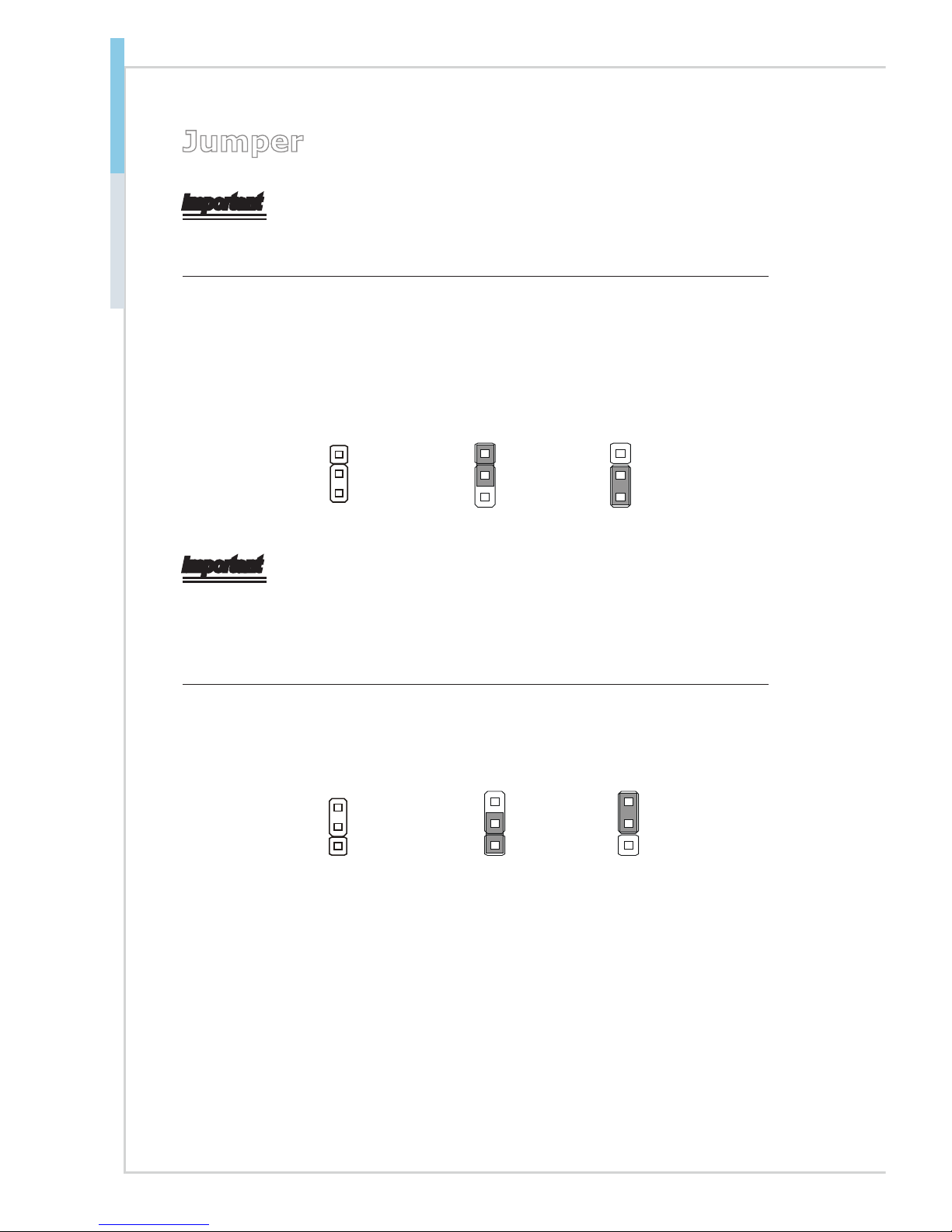
Clear CMOS Jumper: JBAT1
There is a CMOS RAM onboard that has a power supply from an external battery
to keep the data of system configuration. With the CMOS RAM, the system can
automatically boot OS every time it is turned on. If you want to clear the system
configuration, set the jumper to clear data.
Normal
JBAT1
Clear CMOS
111
Important
You can clear CMOS by shorting 2-3 pin while the system is off. Then return to
1-2 pin position. Avoid clearing the CMOS while the system is on; it will damage
the motherboard.
AT/ATX Select Jumper: JAT1
This jumper allows users to select between AT and ATX power.
JAT1
1 11
ATX AT
Page 25
2-15
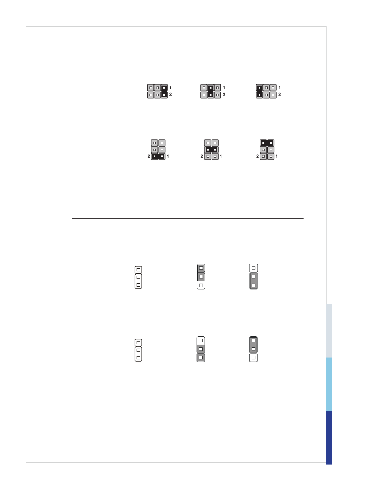
Serial Port Power Jumper: JCOMP1/ JCOMP2
These jumpers specify the operation voltage of the serial ports.
+5V 0V +12V
+5V 0V +12V
JCOMP1
(for COM1)
JCOMP2
(for JCOM2~6)
1
2
1
2
1
2
12 12 12
LVDS Power Jumper: JVDD1/ JVDD2
Use this jumper to specify the operation voltage of the LVDS interface flat panel.
1 1
1
3V
JVDD1
(for JLVDS1)
5V
1 1
1
3V
JVDD2
(for JLVDS2)
5V
Page 26
2-16
Hardware Setup MS-98D1
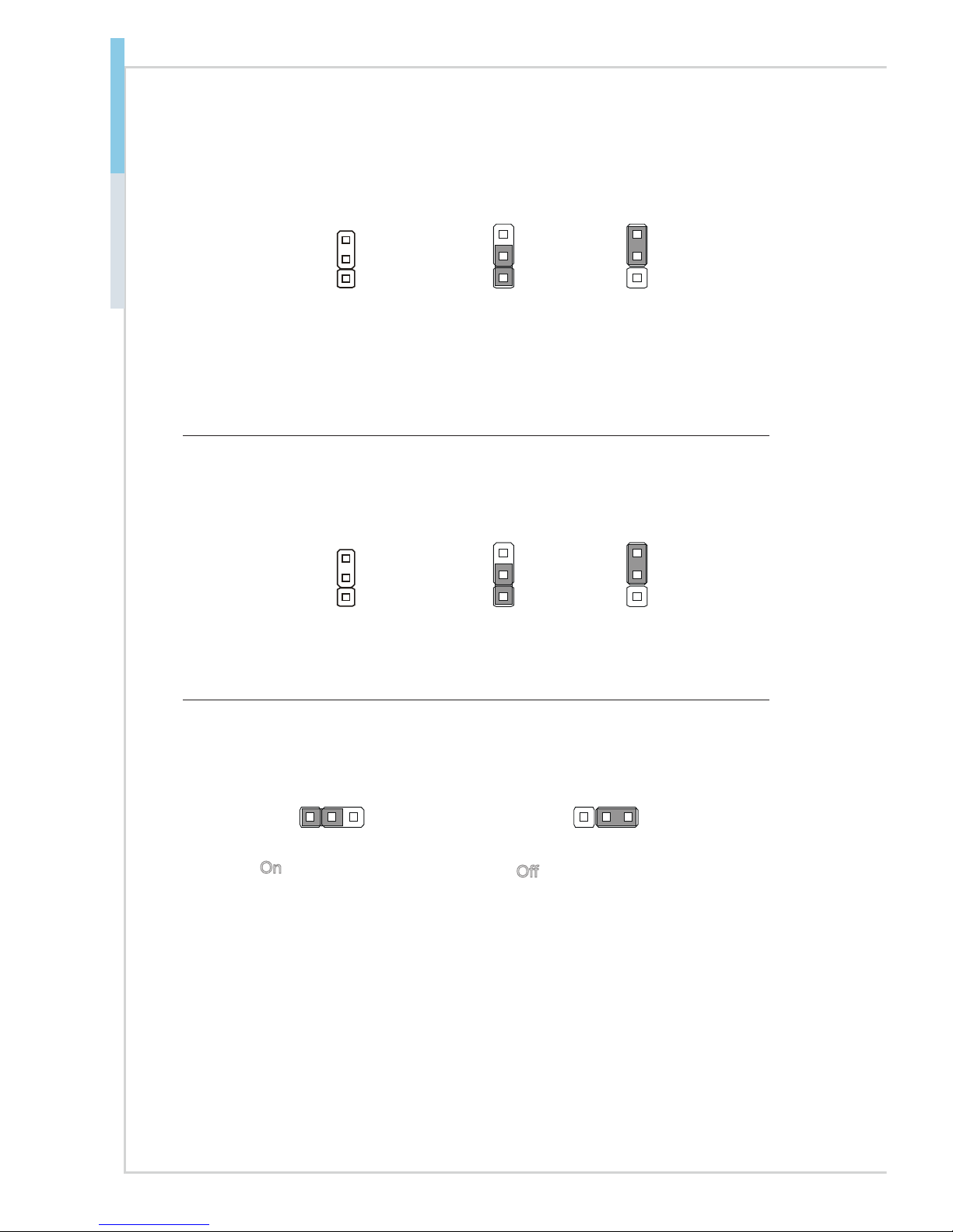
LVDS Inverter Power Jumper: JINV1/ JINV2
Use this jumper to specify the operation voltage of the LVDS interface flat panel.
1 11
5V
JINV1
(for JINVDD1)
JINV2
(for JINVDD2)
12V
PCI-104 Power Jumper: JPCIP1
Use this jumper to specify the operation voltage of the PC/104 slot.
1 11
3V
JPCIP1
5V
NVM LAN Jumper: JNVM1/ JNVM2
Use this jumper to specify the operation for LAN.
1 2 3
JNVM1
(for LAN1)
JNVM2
(for LAN2)
On: Enable security
and the INVM lock.
1 2 3
Off: Disable security and
the INVM lock.
(non-secure mode)
Page 27
2-17
Slot
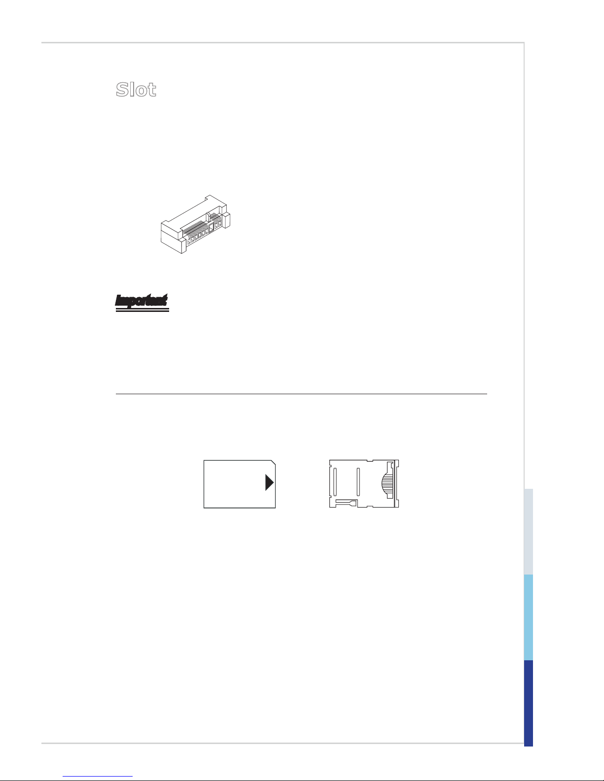
Mini-PCIe (Peripheral Component Interconnect Express)
Slot
The Mini-PCIe slot is provided for wireless LAN card, TV tuner card, Robson
NAND Flash card and mSATA devices.
MINI_PCIE1 supports mSATA function.
MINI_PCIE2 supports 3G module
wireless LAN card, TV tuner card,
Robson NAND Flash card
■
■
Important
When adding or removing expansion cards, make sure that you unplug the power
supply first. Meanwhile, read the documentation for the expansion card to configure any necessary hardware or software settings for the expansion card, such as
jumpers, switches or BIOS configuration.
SIM Card Holder
The holder is provided for SIM card.
SIM card Holder
Page 28
2-18
Hardware Setup MS-98D1
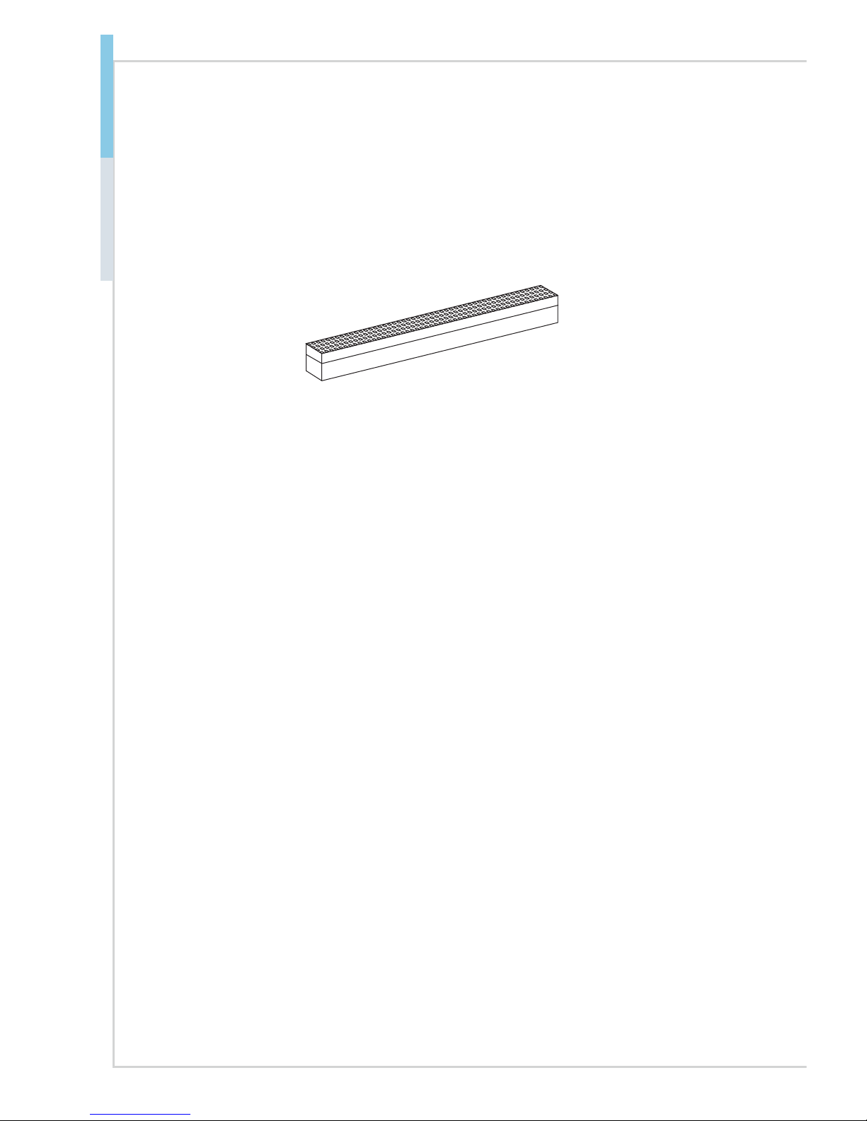
PCI-104 Slot
The PCI-104 computer bus utilizes 104 pins. These pins include all the normal
lines used in the PCI bus, with additional ground pins added to ensure
bus integrity. Signal timing and voltage levels are identical to the PCI bus,
with lower current requirements. The PCI-104 form factor allows modules to
stack together like building blocks.
Page 29

2-3-1
This chapter provides information on the BIOS Setup program and allows
users to configure the system for optimal use.
Users may need to run the Setup program when:
An error message appears on the screen at system startup and requests users to run SETUP.
Users want to change the default settings for customized features.
Important
Please note that BIOS update assumes technician-level experience.
■
■
3 BIOS Setup
Page 30
3-2
BIOS Setup MS-98D1
Entering Setup
Power on the computer and the system will start POST (Power On Self Test)
process. When the message below appears on the screen, press <DEL> or <F2>
key to enter Setup.
Press <DEL> or <F2> to enter SETUP
If the message disappears before you respond and you still wish to enter Setup,
restart the system by turning it OFF and On or pressing the RESET button. You
may also restart the system by simultaneously pressing <Ctrl>, <Alt>, and <Delete> keys.
Important
The items under each BIOS category described in this chapter are under continuous update for better system performance. Therefore, the description may be
slightly different from the latest BIOS and should be held for reference only.
Page 31
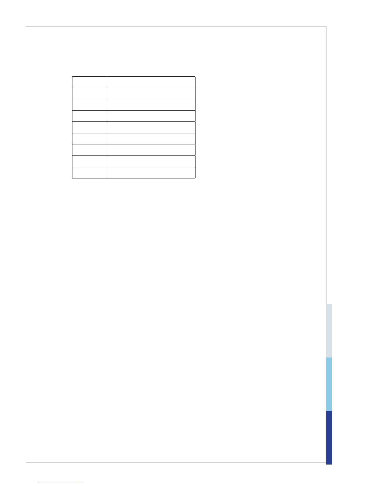
3-3
Control Keys
← → Select Screen
↑ ↓ Select Item
Enter Select
+ - Change Option
F1
General Help
F7 Previous Values
F9 Optimized Defaults
F10 Save & Exit
Esc Exit
Getting Help
After entering the Setup menu, the first menu you will see is the Main Menu.
Main Menu
The main menu lists the setup functions you can make changes to. You can use
the arrow keys ( ↑↓ ) to select the item. The on-line description of the highlighted
setup function is displayed at the bottom of the screen.
Sub-Menu
If you find a right pointer symbol appears to the left of certain fields that means
a sub-menu can be launched from this field. A sub-menu contains additional op-
tions for a field parameter. You can use arrow keys ( ↑↓ ) to highlight the field
and press <Enter> to call up the sub-menu. Then you can use the control keys to
enter values and move from field to field within a sub-menu. If you want to return
to the main menu, just press the <Esc >.
General Help <F1>
The BIOS setup program provides a General Help screen. You can call up this
screen from any menu by simply pressing <F1>. The Help screen lists the appropriate keys to use and the possible selections for the highlighted item. Press
<Esc> to exit the Help screen.
Page 32
3-4
BIOS Setup MS-98D1
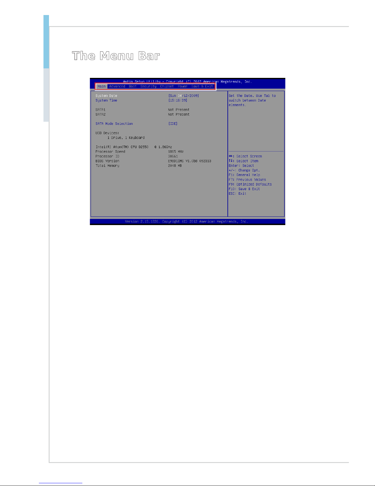
The Menu Bar
Main
Use this menu for basic system configurations, such as time, date, etc.
Advanced
Use this menu to set up the items of special enhanced features.
Boot
Use this menu to specify the priority of boot devices.
Security
Use this menu to set supervisor and user passwords.
Chipset
This menu controls the advanced features of the onboard chipsets.
Power
Use this menu to specify your settings for power management.
Save & Exit
This menu allows you to load the BIOS default values or factory default settings
into the BIOS and exit the BIOS setup utility with or without changes.
▶
▶
▶
▶
▶
▶
▶
Page 33
3-5
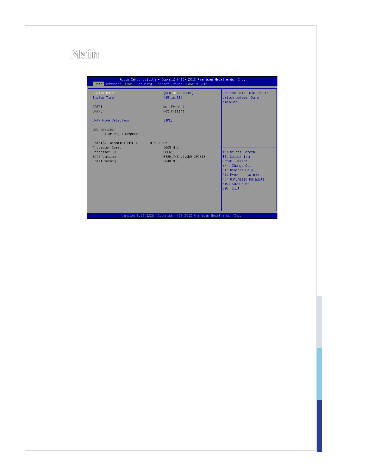
Main
System Date
This setting allows you to set the system date. The date format is <Day>, <Month> <Date> <Year>.
System Time
This setting allows you to set the system time. The time format is <Hour> <Minute> <Second>.
SATA Mode Selection
This setting specifies the SATA controller mode.
▶
▶
▶
Page 34
3-6
BIOS Setup MS-98D1
Advanced
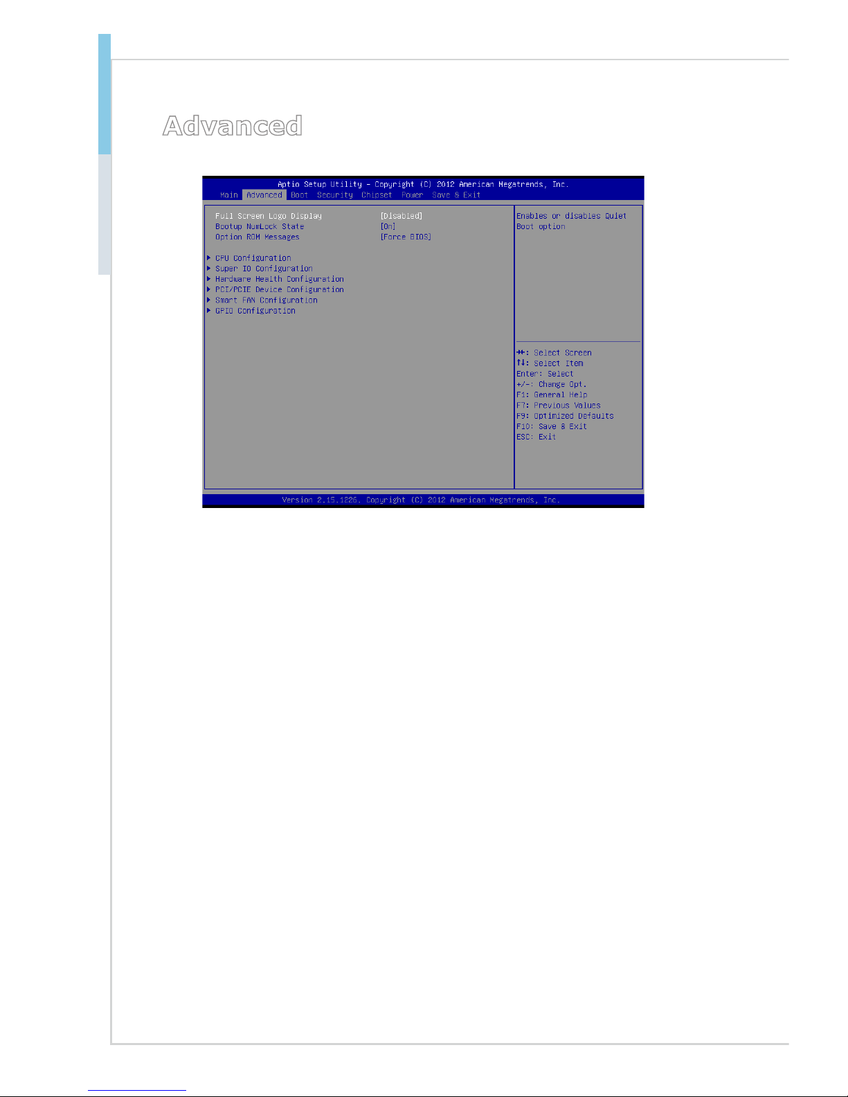
Full Screen Logo Display
This BIOS feature determines if the BIOS should hide the normal POST mes
-
sages with the motherboard or system manufacturer’s full-screen logo.
When it is enabled, the BIOS will display the full-screen logo during the boot-up
sequence, hiding normal POST messages.
When it is disabled, the BIOS will display the normal POST messages, instead
of the full-screen logo.
Please note that enabling this BIOS feature often adds 2-3 seconds of delay to
the booting sequence. This delay ensures that the logo is displayed for a suf
ficient amount of time. Therefore, it is recommended that you disable this BIOS
feature for a faster boot-up time.
Bootup NumLock State
This setting is to set the Num Lock status when the system is powered on. Setting
to [On] will turn on the Num Lock key when the system is powered on. Setting to
[Off] will allow users to use the arrow keys on the numeric keypad.
Option ROM Messages
This item is used to determine the display mode when an optional ROM is ini
tialized during POST. When set to [Force BIOS], the display mode used by AMI
BIOS is used. Select [Keep Current] if you want to use the display mode of optional ROM.
▶
▶
▶
Page 35
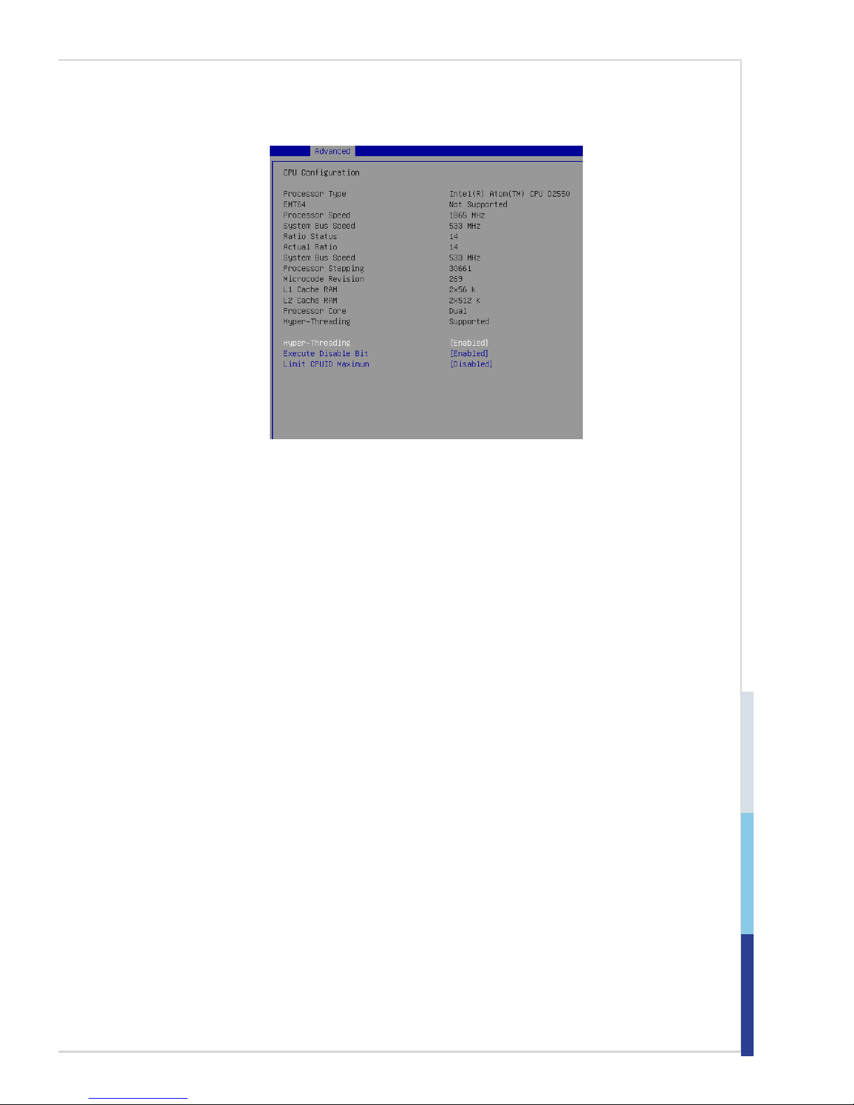
3-7
CPU Configuration
Hyper-Threading
The processor uses Hyper-Threading technology to increase transaction rates
and reduces end-user response times. The technology treats the two cores
inside the processor as two logical processors that can execute instructions
simultaneously. In this way, the system performance is highly improved. If
you disable the function, the processor will use only one core to execute the
instructions. Please disable this item if your operating system doesn’t support
HT Function, or unreliability and instability may occur.
Execute Disable Bit
Intel’s Execute Disable Bit functionality can prevent certain classes of malicious
“buffer overflow” attacks when combined with a supporting operating system.
This functionality allows the processor to classify areas in memory by where
application code can execute and where it cannot. When a malicious worm
attempts to insert code in the buffer, the processor disables code execution,
preventing damage or worm propagation.
Limit CPUID Maximum
The Max CPUID Value Limit BIOS feature allows you to circumvent problems
with older operating systems that do not support the Intel Pentium 4 processor
with Hyper-Threading Technology. When enabled, the processor will limit the
maximum CPUID input value to 03h when queried, even if the processor
supports a higher CPUID input value. When disabled, the processor will return
the actual maximum CPUID input value of the processor when queried.
▶
▶
▶
▶
Page 36
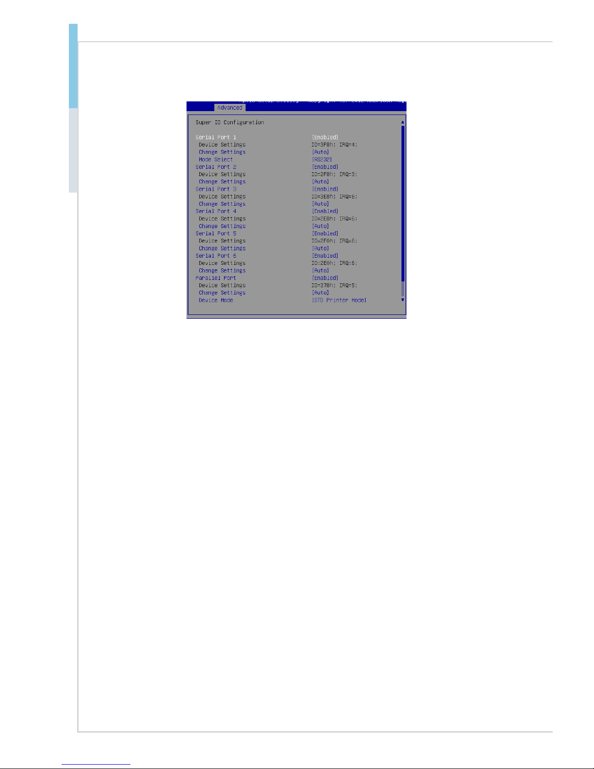
3-8
BIOS Setup MS-98D1
Super IO Configuration
Serial Port 1/ 2/ 3/ 4/ 5/ 6
This setting enables/disables the specified serial port.
Change Settings
This setting is used to change the address & IRQ settings of the specified
serial port.
Mode Select
Select an operation mode for the serial port 1.
Parallel Port
This setting enables/disables the parallel port.
Change Settings
This setting is used to change the address & IRQ settings of the parallel
port.
Device Mode
Select an operation mode for the parallel port.
FIFO Mode
This setting controls the FIFO data transfer mode.
Shared IRQ Mode
This setting provides the system with the ability to share interrupts among its
serial ports.
Watch Dog Timer
You can enable the system watch-dog timer, a hardware timer that generates
a reset when the software that it monitors does not respond as expected each
time the watch dog polls it.
▶
▶
▶
▶
▶
▶
▶
▶
▶
▶
Page 37
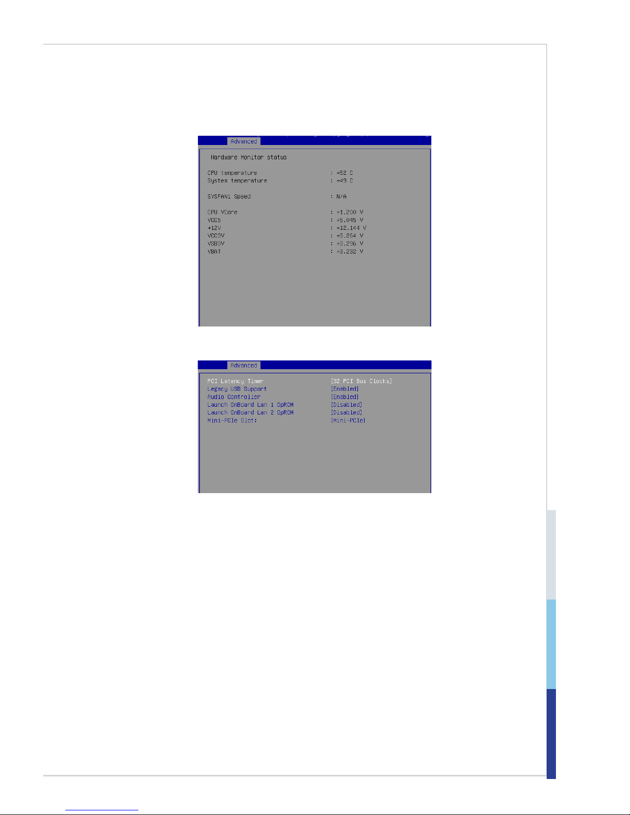
3-9
Hardware Health Configuration
These items display the current status of all monitored hardware devices/
components such as voltages, temperatures and all fans’ speeds.
PCI/PCIE Device Configuration
Legacy USB Support
Set to [Enabled] if you need to use any USB 1.1/2.0 device in the operating
system that does not support or have any USB 1.1/2.0 driver installed, such
as DOS and SCO Unix.
Audio Controller
This setting enables/disables the onboard audio controller.
Launch OnBoard Lan 1/ 2 OpROM
These settings enable/disable the initialization of the onboard LAN1/ 2 Boot
ROM during bootup. Selecting [Disabled] will speed up the boot process.
Mini-PCIe Slot:
Select the operation function for Mini-PCIE1 slot.
▶
▶
▶
▶
▶
▶
Page 38
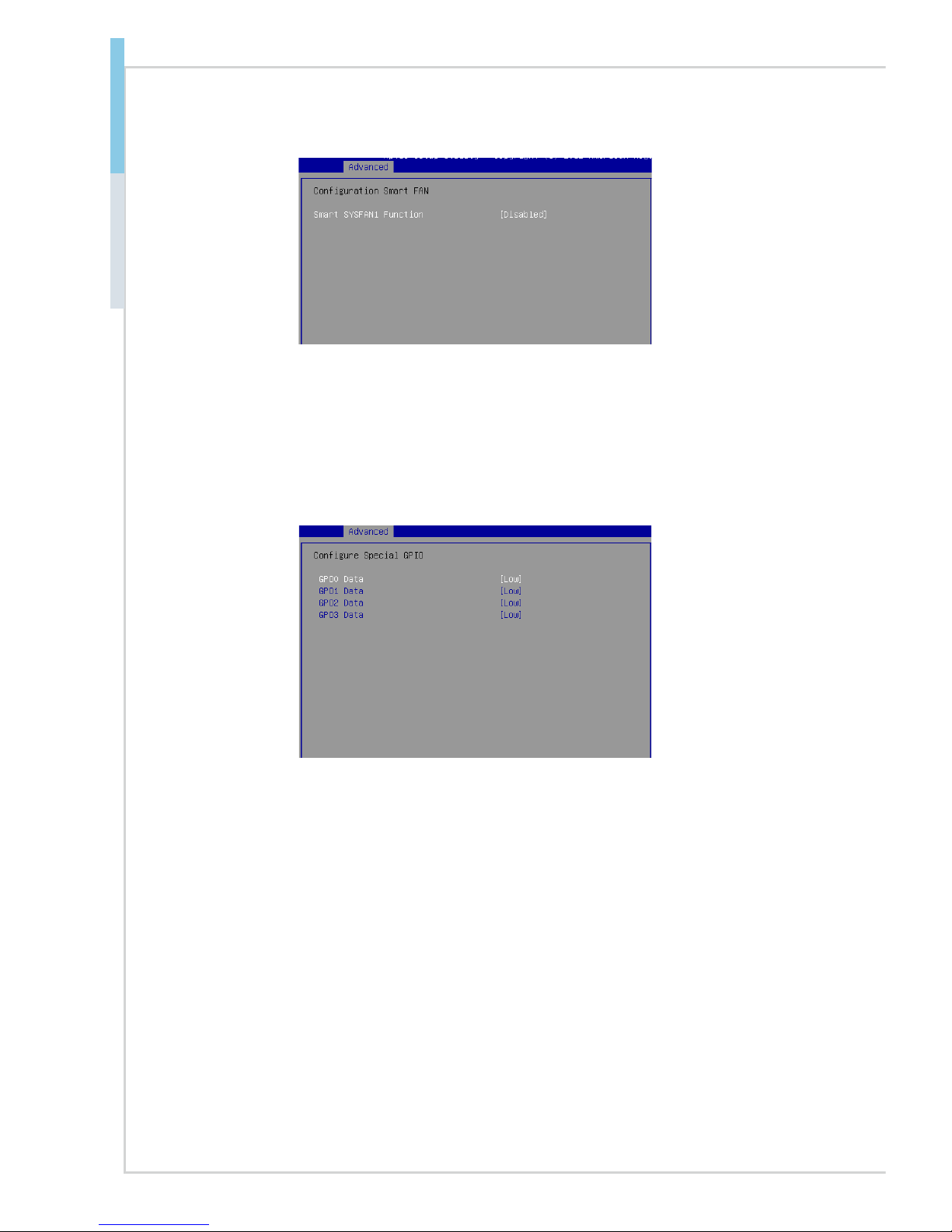
3-10
BIOS Setup MS-98D1
Smart Fan Configuration
Smart SYSFAN1 Function
These settings enable/disable the Smart Fan function. Smart Fan is an
excellent feature which will adjust the CPU/system fan speed automatically
depending on the current CPU/system temperature, avoiding the
overheating to damage your system.
GPIO Configuration
GPO0 ~ GPO3 Data
These settings control the operation mode of the specified GPIO.
▶
▶
▶
▶
Page 39
3-11
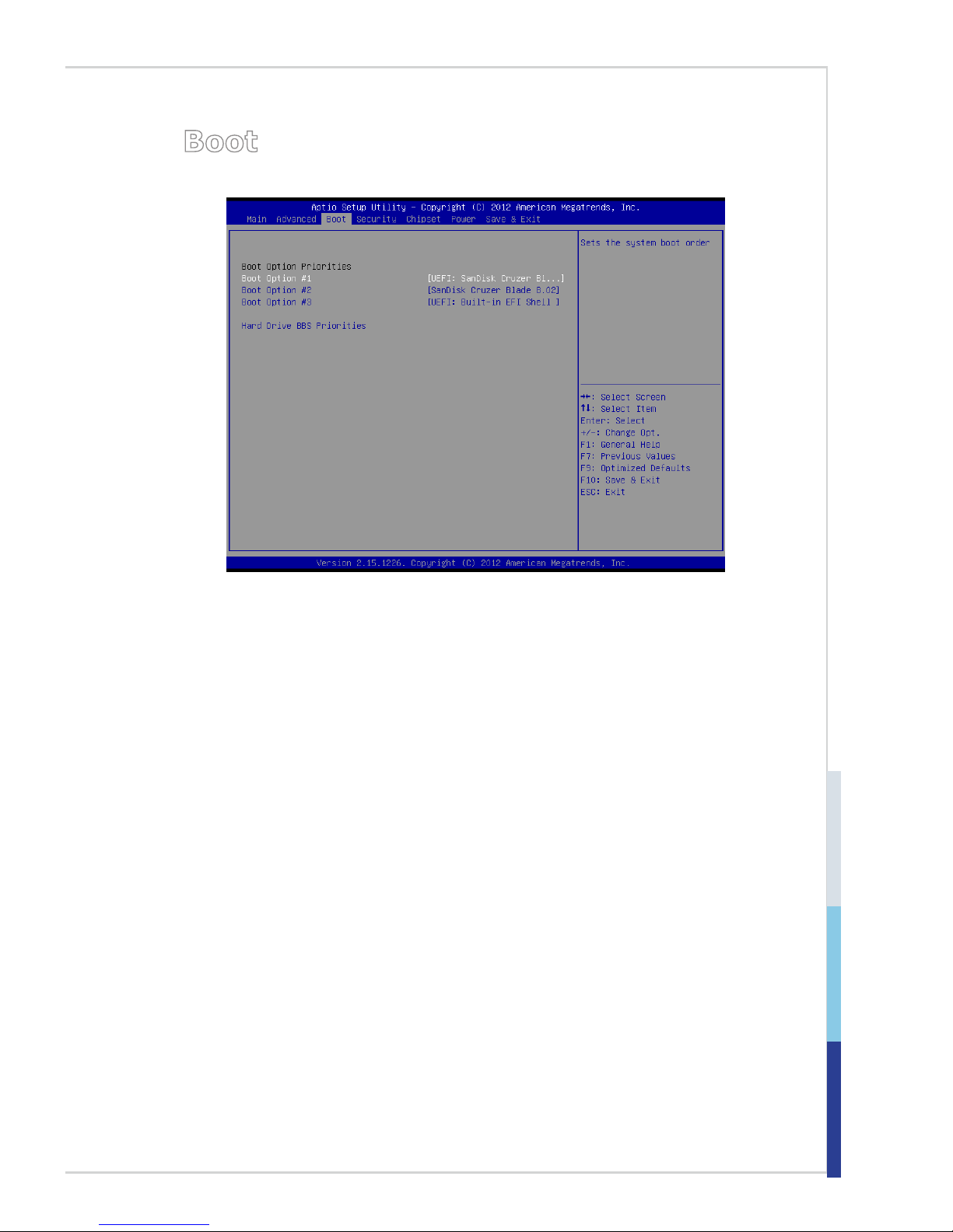
Boot
Boot Option Priorities
This setting allows users to set the sequence of boot devices where BIOS at
tempts to load the disk operating system.
Hard Drive BBS Priorities
This setting allows users to set the priority of the specified devices. First press
<Enter> to enter the sub-menu. Then you may use the arrow keys ( ↑↓ ) to select
the desired device, then press <+>, <-> or <PageUp>, <PageDown> key to move
it up/down in the priority list.
▶
▶
Page 40
3-12
BIOS Setup MS-98D1
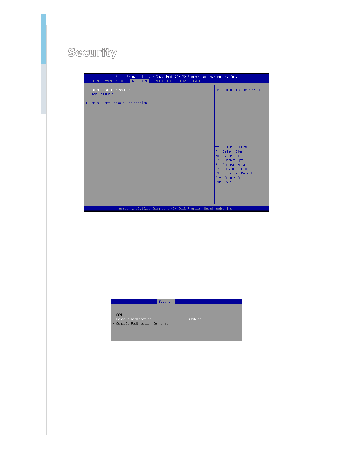
Security
Administrator Password
Administrator Password controls access to the BIOS Setup utility.
User Password
User Password controls access to the system at boot and to the BIOS Setup
utility.
Serial Port Console Redirection
▶
▶
▶
Page 41

3-13
Console Redirection
Console Redirection operates in host systems that do not have a monitor and
keyboard attached. This setting enables/disables the operation of console re
-
direction. When set to [Enabled], BIOS redirects and sends all contents that
should be displayed on the screen to the serial COM port for display on the
terminal screen. Besides, all data received from the serial port is interpreted
as keystrokes from a local keyboard.
Console Redirection Settings
Terminal Type
To operate the system’s console redirection, you need a terminal supporting
ANSI terminal protocol and a RS-232 null modem cable connected between
the host system and terminal(s). This setting specifies the type of terminal
device for console redirection.
Bits per second, Data Bits, Parity, Stop Bits
This setting specifies the transfer rate (bits per second, data bits, parity,
stop bits) of Console Redirection.
Flow Control
Flow control is the process of managing the rate of data transmission be
-
tween two nodes. It’s the process of adjusting the flow of data from one
device to another to ensure that the receiving device can handle all of the
incoming data. This is particularly important where the sending device is capable of sending data much faster than the receiving device can receive it.
VT-UTF8 Combo Key Support
This setting enables/disables the VT-UTF8 combination key support for
ANSI/VT100 terminals.
Recorder Mode, Resolution 100x31
These settings enable/disable the recorder mode and the resolution
100x31.
Legacy OS Redirection Resolution
This setting specifies the redirection resolution of legacy OS.
Putty Keypad
PuTTY is a terminal emulator for Windows. This setting controls the nu
-
meric keypad for use in PuTTY.
▶
▶
▶
▶
▶
▶
▶
▶
▶
Page 42
3-14
BIOS Setup MS-98D1
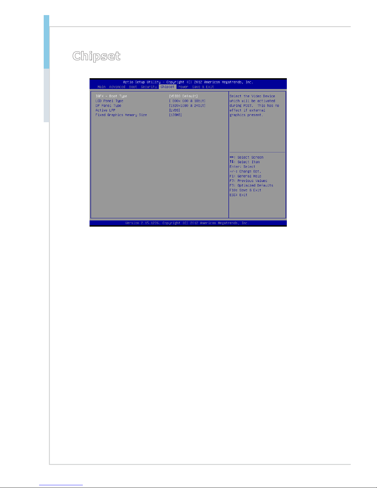
Chipset
IGFX - Boot Type
Use the field to select the type of device you want to use as the boot display of
the system.
LCD Panel Type (LVDS1)
This setting allows you to set the resolution of LCD panel.
DP Panel Type (LVDS2)
This setting allows you to set the resolution of DP panel.
Active LFP
This item is used for turning on/off LVDS support. (LVDS or No LVDS)
Fixed Graphics Memory Size
This setting specifies the size of system memory allocated for video memory.
▶
▶
▶
▶
▶
Page 43
3-15
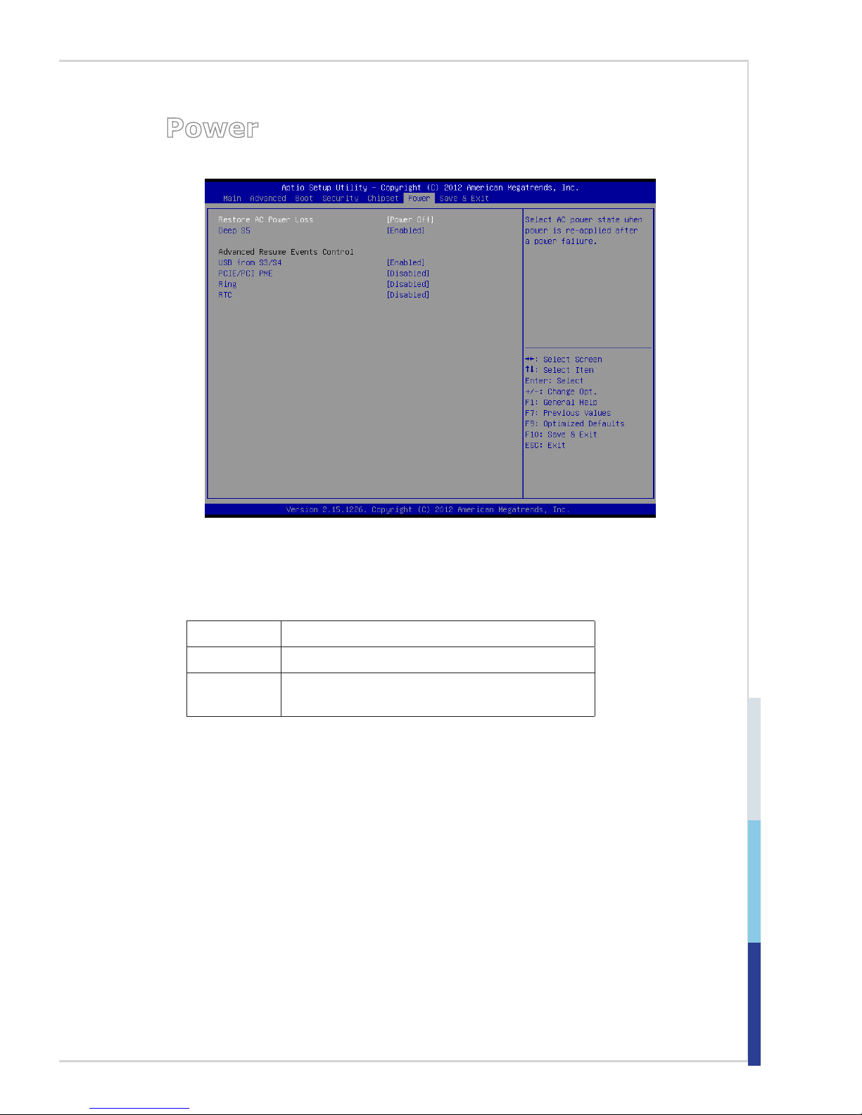
Power
Restore AC Power Loss
This setting specifies whether your system will reboot after a power failure or
interrupt occurs. Available settings are:
[Power Off] Leaves the computer in the power off state.
[Power On] Leaves the computer in the power on state.
[Last State] Restores the system to the previous status
before power failure or interrupt occurred.
Deep S5
The setting enables/disables the Deep S5 power saving mode. S5 is almost
the same as G3 Mechanical Off, except that the PSU still supplies power, at
a minimum, to the power button to allow return to S0. A full reboot is required.
No previous content is retained. Other components may remain powered so the
computer can “wake” on input from the keyboard, clock, modem, LAN, or USB
device.
▶
▶
Page 44

3-16
BIOS Setup MS-98D1
** Advanced Resume Events Control **
USB from S3/S4
The item allows the activity of the USB device to wake up the system from S3/S4
sleep state.
PCIE/PCI PME
This field specifies whether the system will be awakened from power saving
modes when activity or input signal of onboard PCIE/PCI PME is detected.
Ring
An input signal on the serial Ring Indicator (RI) line (in other words, an incoming
call on the modem) awakens the system from a soft off state.
RTC
When [Enabled], your can set the date and time at which the RTC (real-time
clock) alarm awakens the system from suspend mode.
▶
▶
▶
▶
Page 45
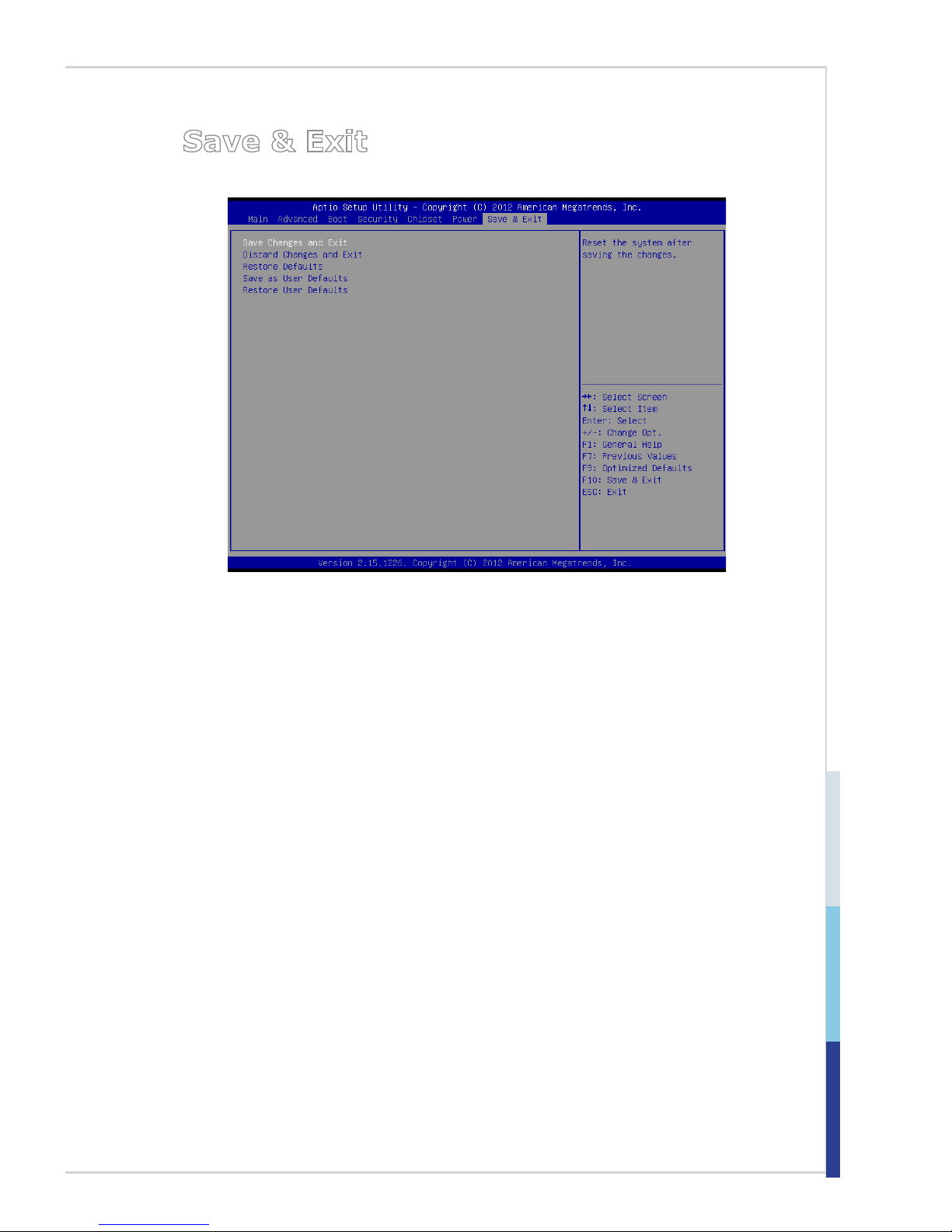
3-17
Save & Exit
Save Changes and Exit
Save changes to CMOS and exit the Setup Utility.
Discard Changes and Exit
Abandon all changes and exit the Setup Utility.
Restore Defaults
Restore the factory defaults.
Save as User Defaults
Save changes as the user’s default profile.
Restore User Defaults
Restore the user’s default profile.
▶
▶
▶
▶
▶
Page 46

Page 47

2-A-1
This appendix provides the sample codes of WDT (Watch Dog Timer)
and GPIO (General Purpose Input/ Output).
A WDT & GPIO
Page 48
A-2
WDT & GPIO MS-98D1
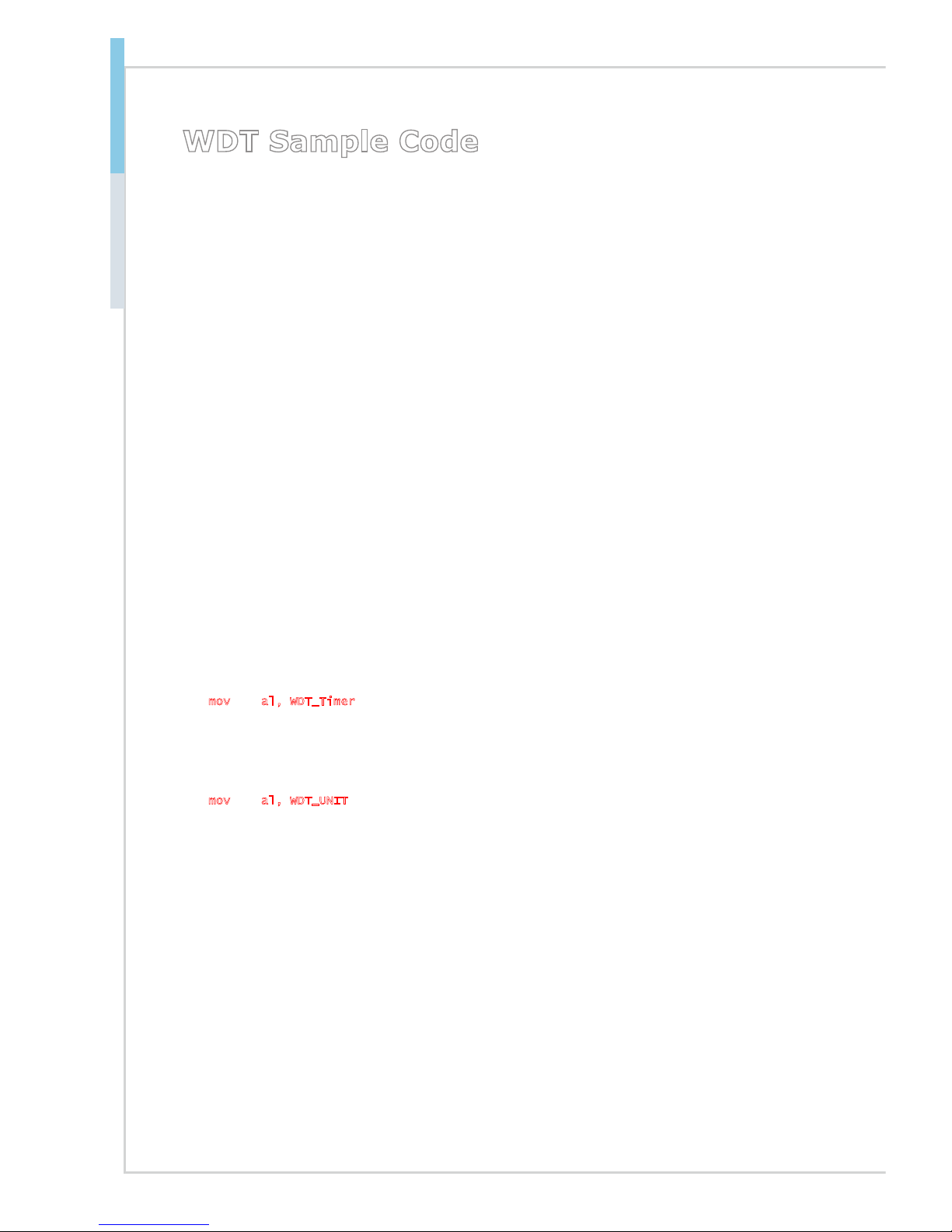
WDT Sample Code
SIO_INDEX_Port equ 04Eh
SIO_DATA_Port equ 04Fh
SIO_UnLock_Value equ 087h
SIO_Lock_Value equ 0AAh
WatchDog_LDN equ 007h
WDT_UNIT equ 60h ;60h=second, 68h=minute, 40h=Disabled Watchdog timer
WDT_Timer equ 30 ;ex. 30 seconds
Sample code:
;Enable config mode
mov dx, SIO_INDEX_Port
mov al, SIO_UnLock_Value
out dx, al
jmp short $+2 ;Io_delay
jmp short $+2 ;Io_delay
out dx, al
;Change to WDT
mov dx, SIO_INDEX_Port
mov al, 07h
out dx, al
mov dx, SIO_DATA_Port
mov al, WatchDog_LDN
out dx, al
;Acive WDT
mov dx, SIO_INDEX_Port
mov al, 30h
out dx, al
mov dx, SIO_DATA_Port
in al, dx
or al, 01h
out dx, al
;set timer
mov dx, SIO_INDEX_Port
mov al, 0F6h
out dx, al
mov dx, SIO_DATA_Port
mov al, WDT_Timer
out dx, al
;set UINT
mov dx, SIO_INDEX_Port
mov al, 0F5h
out dx, al
mov dx, SIO_DATA_Port
mov al, WDT_UNIT
out dx, al
;enable reset
mov dx, SIO_INDEX_Port
mov al, 0FAh
out dx, al
mov dx, SIO_DATA_Port
in al, dx
or al, 01h
out dx, al
;close config mode
mov dx, SIO_INDEX_Port
mov al, SIO_Lock_Value
out dx, al
Page 49
A-3
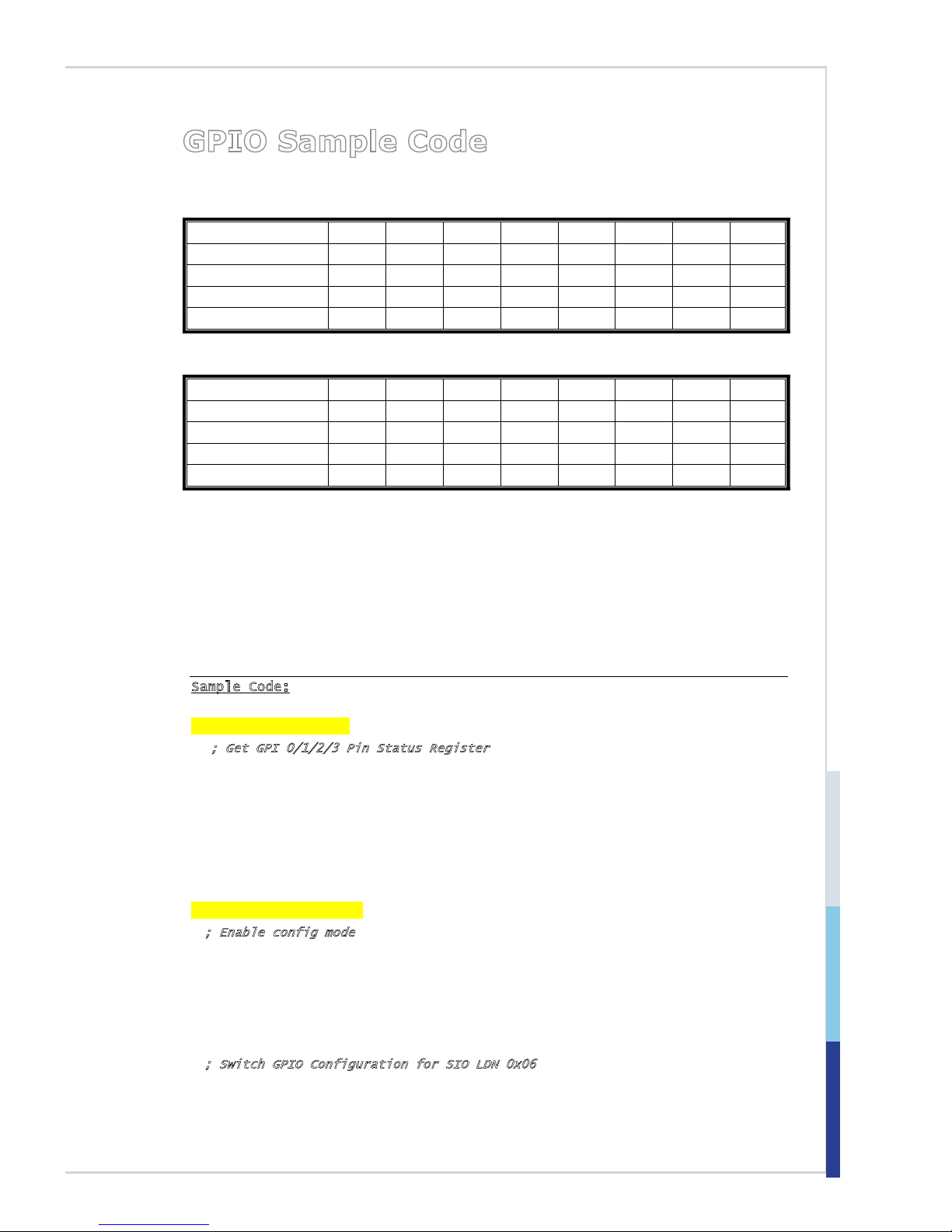
GPIO Sample Code
GPI 0 ~ GPI 3
GPI 0
GPI 1
GPI 2
GPI 3
IO Address
50Ch
50Ch
50Ch
50Ch
SIO GPIO Register
Bit 2 3 4 5
Sample code
#1
GPO 0 ~ GPO 3
GPO 0
GPO 1
GPO 2
GPO 3
IO Address
SIO GPIO Register
F1h
F1h
F1h
F1h
Bit 4 1 2 3
Sample code
#2
SIO_INDEX_Port equ 04Eh
SIO_DATA_Port equ 04Fh
SIO_UnLock_Value equ 087h
SIO_Lock_Value equ 0AAh
SIO_LDN_GPIO equ 06h
GPO_REG equ 0F1h
GPO_0 equ 00010000b
Sample Code:
#1 : Get GPI 0 status
; Get GPI 0/1/2/3 Pin Status Register
mov dx, 50Ch
in eax, dx
;eax bit2 = GPI 0 status
;eax bit3 = GPI 1 status
;eax bit4 = GPI 2 status
;eax bit5 = GPI 3 status
#2 : Set GPO 0 to high
; Enable config mode
mov dx, SIO_INDEX_Port
mov al, SIO_UnLock_Value
out dx, al
jmp short $+2 ;Io_delay
jmp short $+2 ;Io_delay
out dx, al
; Switch GPIO Configuration for SIO LDN 0x06
Page 50

A-4
WDT & GPIO MS-98D1
mov dx, SIO_INDEX_Port
mov al, 07h
out dx, al
mov dx, SIO_DATA_Port
mov al, SIO_LDN_GPIO
out dx, al
; Set GPO 0 Register
mov dx, SIO_INDEX_Port
mov al, GPO_REG
out dx, al
mov dx, SIO_DATA_Port
in al, dx
and al, not GPO_0
;clear al bit4 (GPO 0)
or al, GPO_0
;set GPO 0
out dx, al
;
Exit SIO
mov dx, SIO_INDEX_Port
mov al, SIO_Lock_Value
out dx, al
 Loading...