

Page 1
i
G52-M7043X1
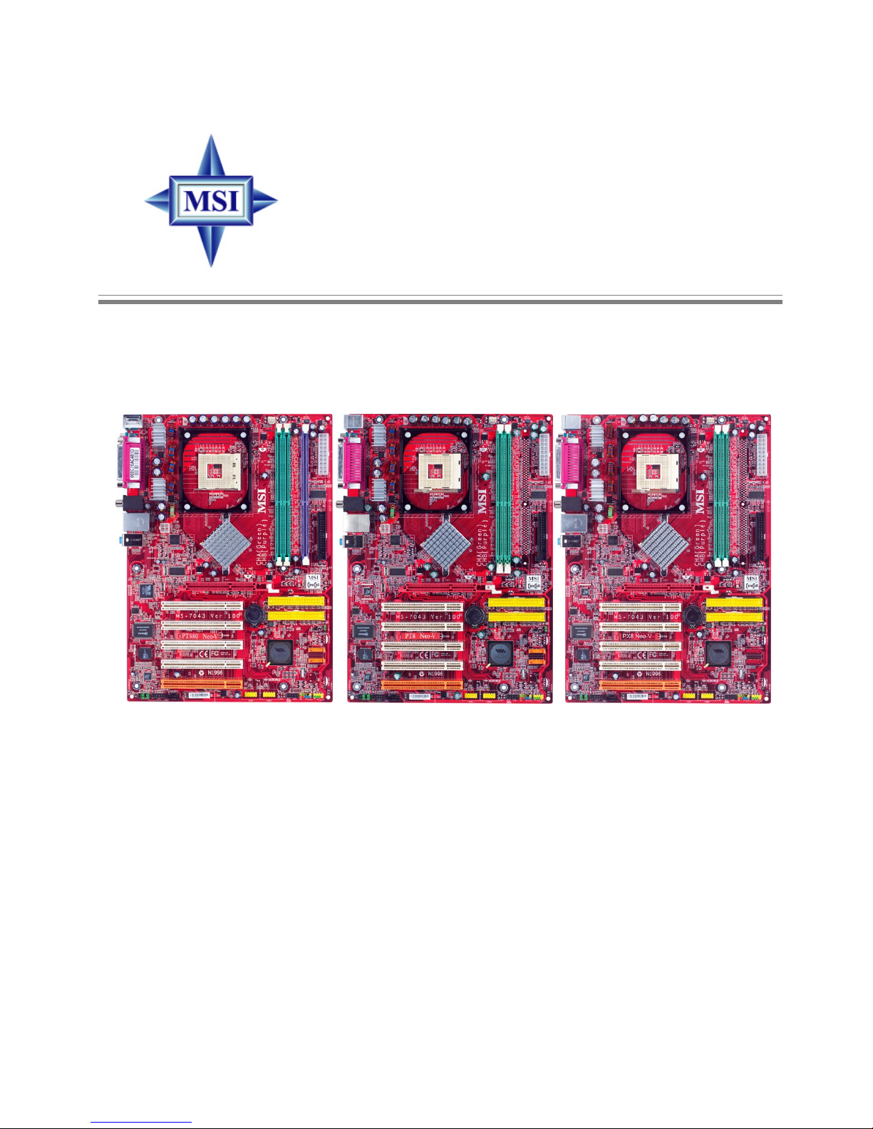
PT880 Neo-V/PT8 Neo-V/PX8 Neo-V
MS-7043 (v1.X) A TX Mainboard
PT880 Neo-V PT8 Neo-V PX8 Neo-V
Page 2

ii
Manual Rev: 1.0
Release Date: March 2004
FCC-A Radio Frequency Interference Statement
This equipment has been tested and found to comply with the limits for a class
A digital device, pursuant to part 15 of the FCC rules. These limits are designed
to provide reasonable protection against harmful interference when the equipment is operated in a commercial environment. This equipment generates, uses
and can radiate radio frequency energy and, if not installed and used in accordance with the instruction manual, may cause harmful interference to radio
communications. Operation of this equipment in a residential area is likely to
cause harmful interference, in which case the user will be required to correct
the interference at his own expense.
Notice 1
The changes or modifications not expressly approved by the party responsible for compliance could void the user’s authority to operate the equipment.
Notice 2
Shielded interface cables and A.C. power cord, if any, must be used in order to
comply with the emission limits.
VOIR LA NOTICE D’INSTALLATION AVANT DE RACCORDER AU
RESEAU.
Micro-Star International
MS-7043
This device complies with Part 15 of the FCC Rules. Operation is subject to
the following two conditions:
(1) this device may not cause harmful interference, and
(2) this device must accept any interference received, including interference
that may cause undesired operation.
Page 3

iii
Copyright Notice
The material in this document is the intellectual property of MICRO-STAR
INTERNATIONAL. W e take every care in the preparation of this document,
but no guarantee is given as to the correctness of its contents. Our products
are under continual improvement and we reserve the right to make changes
without notice.
Trademarks
All trademarks are the properties of their respective owners.
Intel® and Pentium® are registered trademarks of Intel Corporation.
PS/2 and OS®/2 are registered trademarks of International Business Machines
Corporation.
Windows® 95/98/2000/NT/XP are registered trademarks of Microsoft
Corporation.
Netware® is a registered trademark of Novell, Inc.
Award® is a registered trademark of Phoenix T echnologies Ltd.
AMI® is a registered trademark of American Megatrends Inc.
Revision History
Revision Revision History Date
V1.0 First release for PCB 1.X March 2004
Technical Support
If a problem arises with your system and no solution can be obtained from the
user’s manual, please contact your place of purchase or local distributor.
Alternatively, please try the following help resources for further guidance.
V isit the MSI website for FAQ, technical guide, BIOS updates, driver
updates, and other information: http://www.msi.com.tw/program/ser-
vice/faq/faq/esc_faq_list.php
Contact our technical staff at: [email protected]
Page 4

iv
1. Always read the safety instructions carefully.
2. Keep this User’s Manual for future reference.
3. Keep this equipment away from humidity.
4. Lay this equipment on a reliable flat surface before setting it up.
5. The openings on the enclosure are for air convection hence protects the equipment from overheating. DO NOT COVER THE OPENINGS.
6. Make sure the voltage of the power source and adjust properly 110/220V before
connecting the equipment to the power inlet.
7. Place the power cord such a way that people can not step on it. Do not place
anything over the power cord.
8. Always Unplug the Power Cord before inserting any add-on card or module.
9. All cautions and warnings on the equipment should be noted.
10. Never pour any liquid into the opening that could damage or cause electrical
shock.
11. If any of the following situations arises, get the equipment checked by a service
personnel:
††
††
† The power cord or plug is damaged.
††
††
† Liquid has penetrated into the equipment.
††
††
† The equipment has been exposed to moisture.
††
††
† The equipment has not work well or you can not get it work according to User’s
Manual.
††
††
† The equipment has dropped and damaged.
††
††
† The equipment has obvious sign of breakage.
12. DO NOT LEAVE THIS EQUIPMENT IN AN ENVIRONMENT UNCONDITIONED, STORAGE
TEMPERA TURE ABOVE 600 C (1400F), IT MAY DAMAGE THE EQUIPMENT.
Safety Instructions
CAUTION: Danger of explosion if battery is incorrectly replaced.
Replace only with the same or equivalent type recommended by the manufacturer.
Page 5

v
CONTENTS
Copyright Notice ............................................................................................................ iii
Trademarks.................................................................................................................... iii
Technical Support.......................................................................................................... iii
Safety Instructions ........................................................................................................ v
Getting Started ........................................................................................................ 2-1
Mainboard Specifications ...................................................................................2-2
Mainboard Layout ...............................................................................................2-4
Back Pa nel...........................................................................................................2-7
Chapter 2. Hardware Setup .................................................................................. 2-1
Central Processing Unit: CPU.............................................................................. 2-2
CPU Core Speed Derivation Procedure ...................................................... 2-3
Memory Speed/CPU FSB Support Matrix ...................................................2-3
Installing the CPU Fan .................................................................................2-4
Memory ...............................................................................................................2-5
Memory Population Rules............................................................................ 2-5
Power Supply .....................................................................................................2-6
ATX 20-Pin Power Connector: ATX1 .......................................................... 2-6
ATX 12V Power Connector: JPW1.............................................................2-6
Connectors .........................................................................................................2-7
Floppy Disk Drive Connector: FDD1 ............................................................2-7
S-Bracket (SPDIF) Connector: JSP1 (Optional) .......................................... 2-7
Chassis Intrusion Switch Connector: JCI1 (Optional) ................................2-8
CD-In Connector: JCD1 ...............................................................................2-8
Serial ATA RAID 0, 1 Connectors: SATA1, SATA2 (for PT880/PT8 Neo-V) 2-8
Fan Power Connector: CPUFA1 ................................................................ 2-9
D-Bracket™ 2 Connector: JDB1 (Optional) ................................................2-9
Hard Disk Connectors: IDE1 & IDE2 ..........................................................2-10
Front Panel Connectors: JFP1 & JFP2 ...................................................... 2-10
Front USB Connectors: JUSB1 & JUSB2 ................................................. 2-11
Jumpers ............................................................................................................ 2-12
Clear CMOS Jumper: JBAT1 ..................................................................... 2-12
Front Panel Audio Connector: JAUD1.......................................................2-12
Slots ..................................................................................................................2-13
PCI Interrupt Request Routing ...................................................................2-13
AGP (Accelerated Graphics Port) Slot .....................................................2-13
PCI (Peripheral Component Interconnect) Slots ....................................... 2-13
Chapter 3. BIOS Setup ............................................................................................ 3-1
The Main M enu.................................................................................................... 3-2
Frequency/Voltage Control................................................................................. 3-3
Page 6

1-1
Getting Started
Getting Started
Thank you for choosing the MS-7043 (PT880 Neo-V/PT8 NeoV/PX8 Neo-V) v1.X ATX mainboards. The MS-7043 series are
superior computer mainboards based on VIA® PT880/PT800/P4X533
Northbridge & VT8237 Southbridge for optimal system efficiency.
Designed to fit the advanced Intel® Pentium® 4 processors in 478
pin package, the MS-7043 series deliver a high performance and
professional desktop platform solution.
Page 7

1-2
MS-7043 ATX Mainboard
Mainboard Specifications
CPU
h Supports Intel® P4 Northwood/Prescott (Socket 478) processors
h FSB 400 (for Northwood only), 533, 800 (for PT880/PT800 only) MHz
h Supports up to 3.4GHz or higher speed (Please refer to the latest online news at
http://www.msi.com.tw/program/products/mainboard/mbd/
pro_mbd_cpu_support.php)
Chipset
h VIA® PT880 chipset (for PT880 Neo-V)
- Supports FSB 800/533/400MHz
- Supports AGP 8X interface
- Supports DDR 400/333/266 memory interface
h VIA® PT800 chipset (for PT8 Neo-V)
- Supports FSB 800/533/400MHz
- Supports AGP 8X interface
- Supports DDR 400/333/266 memory interface
h VIA® P4X533 chipset (for PX8 Neo-V)
- Supports FSB 533/400MHz
- Supports AGP 8X interface
- Supports DDR 333/266 memory interface
h VIA® VT8237 chipset
- High Bandwidth V-link Client controller
- Integrated Faster Ethernet LPC
- Integrated Hardware Sound Blaster/Direct Sound AC97 audio
- Ultra DMA 66/100/133 master mode PCI EIDE controller
- ACPI
- Supports Serial ATA
- Supports USB2.0
PT880 Neo-V Main Memory
h Supports six memory banks using three 184-pin DDR DIMMs
h Supports dual-channel memory
h Supports a maximum memory size up to 3GB
h Supports 2.5v DDR SDRAM DIMM
PT8 Neo-V/PX8 Neo-V Main Memory
h Supports four memory banks using two 184-pin DDR DIMMs
h Supports single-channel memory
h Supports a maximum memory size up to 2GB
h Supports 2.5v DDR SDRAM DIMM
Slots
h One AGP (Accelerated Graphics Port) slot supports 8x/4x (AGP 3.0) at 1.5V (3.
3V not supported)
h Five 32-bit Master PCI bus slots (support 3.3v/5v PCI bus interface)
Page 8

1-3
Getting Started
Onboard IDE
h An IDE controller integrated in the VIA® VT8237 chipset
- Supports IDE HDD/CD-ROM with PIO, Bus Master and Ultra DMA 66/100/133
operation modes
- Can connect up to four Ultra ATA drives
Onboard Serial ATA (for PT880 Neo-V/PT8 Neo-V)
h Serial ATA/150 controller integrated in the VIA® VT8237 chipset
- Up to 150MB/sec transfer rate
- Can connect up to two Serial ATA drives
USB Interface
h 8 USB ports
- Controlled by VT8237 southbridge
- 4 ports in the rear I/O, 4 ports via the external bracket
On-Board Peripherals
h On-Board Peripherals include:
- 1 floppy port supports 2 FDDs with 360K, 720K, 1.2M, 1.44M and
2.88Mbytes
- 1 serial port (COM A)
- 1 parallel port supports SPP/EPP/ECP mode
- 8 USB 2.0 ports (Rear x 4 / Front x 4)
- 1 RJ45 LAN jack
- 1 D-Bracket2 pinheader (Optional)
- 1 S-Bracket pinheader (Optional)
- 1 Line-In / Line-Out /Mic
- 1 Coaxial SPDIF out (Optional)
Audio
h AC97 link controller integrated in VT8237
h VIA® VT1617 6-channel audio codec
- Compliance with AC97 v2.2 Spec
- Meets PC2001 audio performance requirement
PT880 Neo-V LAN
h VIA® VT8237 integrated MAC
h VIA® VT6122 Gigabit LAN controller
PT8 Neo-V/PX8 Neo-V LAN
h VIA® VT8237 integrated MAC
h VIA® VT6103L 10/100 PHY
BIOS
h The mainboard BIOS provides “Plug & Play” BIOS which detects the peripheral
devices and expansion cards of the board automatically
h The mainboard provides a Desktop Management Interface (DMI) function which
records your mainboard specifications
Dimension
h ATX Form Factor: 30.5cm x 19.5cm
Mounting
h 6 standard mounting holes
Page 9
1-4
MS-7043 ATX Mainboard
Mainboard Layout
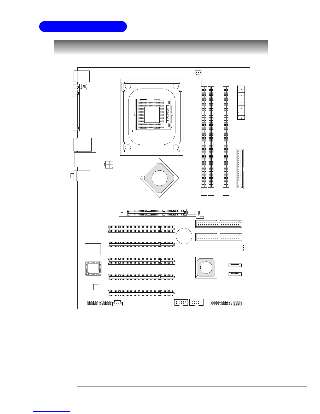
PT880 Neo-V (MS-7043 v1.X) ATX Mainboard
- VIA® PT880 Northbridge
- VIA® VT6122 Gigabit LAN
- 2 Serial ATA connectors
- 3 DDR DIMMs up to 3 GB
BATT
+
D
I
M
M
1
D
I
M
M
3
D
I
M
M
2
JAUD1 JSP1
JUSB2
A
T
X
1
CPUFA1
SATA1
SATA2
JFP1
JDB1
JFP2
VIA
Audio Codec
VT1617
Winbond
W83697HF
VIA
Gigabit LAN
VT6122
BIOS
PCI 5
PCI 4
PCI 3
PCI 2
PCI 1
IDE 2
IDE 1
JPW1
Top :
Parallel Port
Bottom:
COM A
Top : Mous e
Bottom: Keyboard
T : LAN Jack
B: USB Po r ts
JCD1
F
D
D
1
AGP1
JBAT1
JUSB1
T: SPD IF Out
B: USB Po r ts
T:
M:
B: Mic
Line-In
Line-Out
VIA
VT8237
VIA
PT880
Page 10
1-5
Getting Started
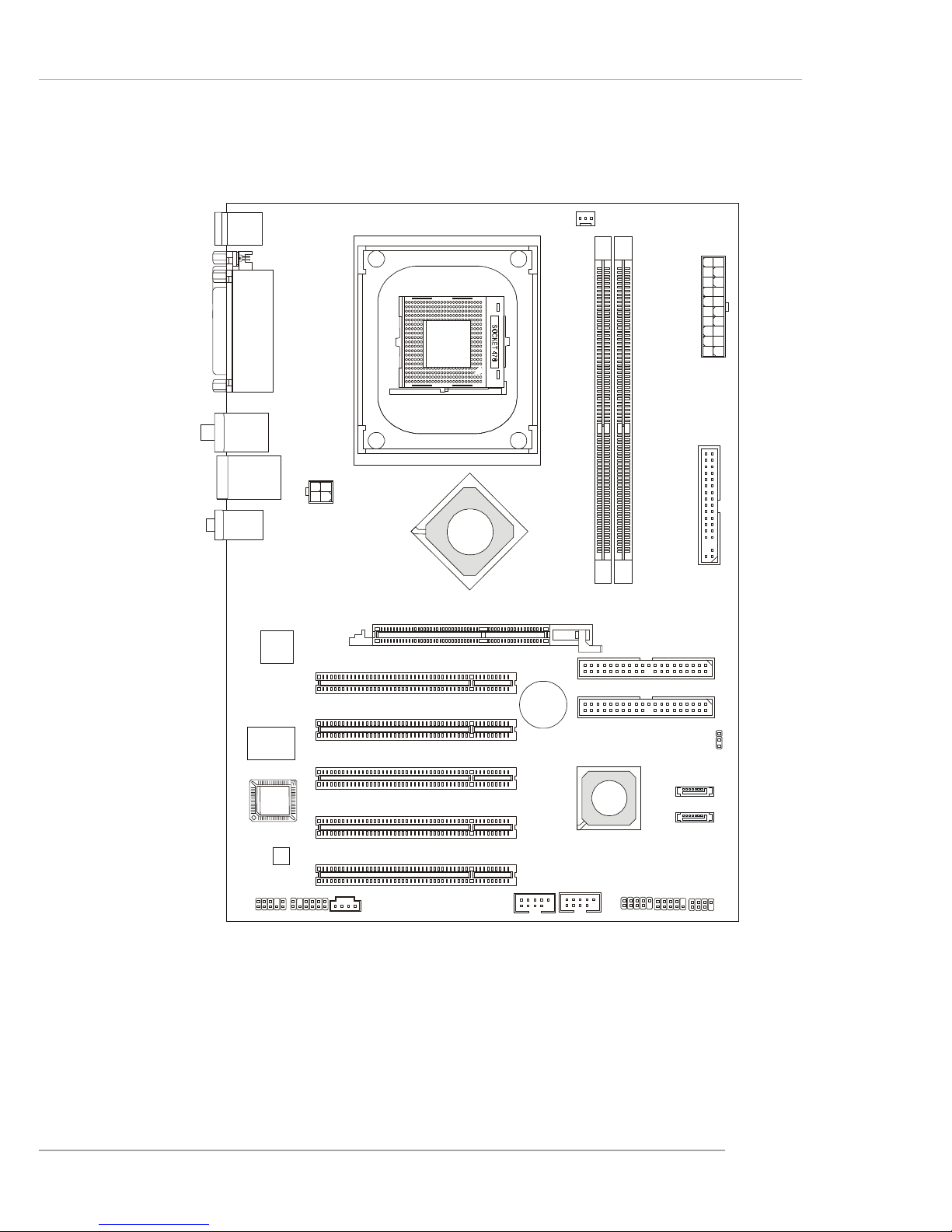
PT8 Neo-V (MS-7043 v1.X) ATX Mainboard
- VIA® PT800 Northbridge
- VIA® VT6103L 10/100Mbps LAN
- 2 Serial ATA connectors
- 2 DDR DIMMs up to 2 GB
BATT
+
D
I
M
M
1
D
I
M
M
2
JAUD1 JSP1
JUSB2
A
T
X
1
CPUFA1
SATA1
SATA2
JFP1
JDB1
JFP2
VIA
Audio Codec
VT1617
Winbond
W83697HF
VIA
10/100 LAN
VT6103L
BIOS
PCI 5
PCI 4
PCI 3
PCI 2
PCI 1
IDE 2
IDE 1
JPW1
Top :
Parallel Port
Bottom:
COM A
Top : Mous e
Bottom: Keyboard
T : LAN Jack
B: USB Po rts
JCD1
F
D
D
1
AGP1
JBAT1
JUSB1
T: SPD IF Out
B: USB Po rts
T:
M:
B: Mic
Line-In
Line-Out
VIA
VT8237
VIA
PT800
Page 11
1-6
MS-7043 ATX Mainboard
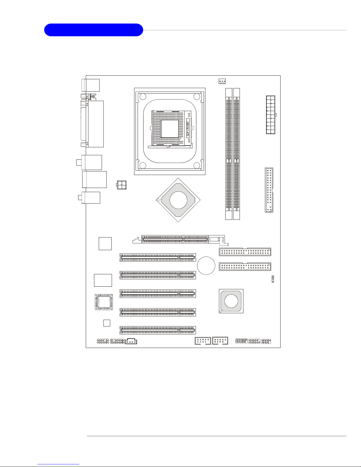
PX8 Neo-V (MS-7043 v1.X) ATX Mainboard
- VIA® P4X533 Northbridge
- VIA® VT6103L 10/100Mbps LAN
- 2 DDR DIMMs up to 2 GB
BATT
+
D
I
M
M
1
D
I
M
M
2
JAUD1 JSP1
JUSB2
A
T
X
1
CPUFA1
JFP1
JDB1
JFP2
VIA
Audio Codec
VT1617
Winbond
W83697HF
VIA
10/100 LAN
VT6103L
BIOS
PCI 5
PCI 4
PCI 3
PCI 2
PCI 1
IDE 2
IDE 1
JPW1
Top :
Parallel Port
Bottom:
COM A
Top : Mous e
Bottom: Keyboard
T : LAN Jack
B: USB Po r ts
JCD1
F
D
D
1
AGP1
JBAT1
JUSB1
T: SPD IF Out
B: USB Po r ts
T:
M:
B: Mic
Line-In
Line-Out
VIA
VT8237
VIA
P4X533
Page 12
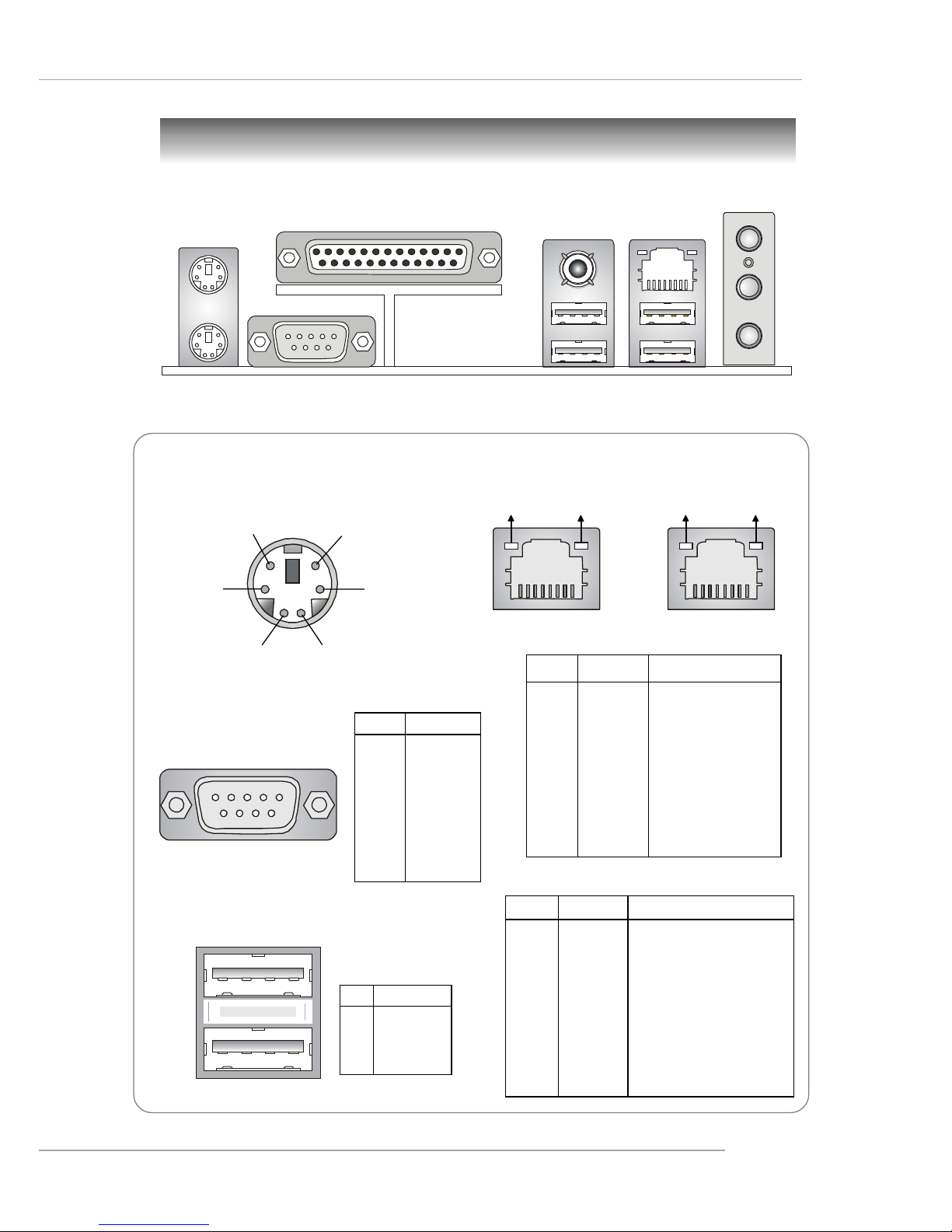
1-7
Getting Started
Back Panel
Mouse/Keyboard Connector
Pin1
Mouse/KBD
DATA
Pin2 NC
Pin3 GNDPin4 VCC
Pin5
Mouse/KBD Clock
Pin6 NC
USB Ports
1 2 3 4
PIN SIGNAL
1 VCC
2 -Data
3 +Data
4 GND
RJ-45 LAN Jack
Serial Port
PIN SIGNAL
1 DCD
2 SIN
3 SOUT
4 DTR
5 GND
6 DSR
7 RTS
8 CTS
9RI
1 2 3 4 5
6 7 8 9
Gigabit LAN (for PT880 Neo-V)
PIN SIGNAL DESCRIPTION
1 D0P Differential Pair 0+
2 D0N Differential Pair 03 D1P Differential Pair 1+
4 D2P Differential Pair 2+
5 D2N Differential Pair 26 D1N Differential Pair 17 D3P Differential Pair 3+
8 D3N Differential Pair 3-
10/100 LAN (for PT8 Neo-V/PX8 Neo-V)
PIN SIGNAL DESCRIPTION
1 TD P Transmit Differential Pair
2 TDN Transmit Differential Pair
3 RDP Receive Differential Pair
4 NC Not Used
5 NC Not Used
6 RDN Receive Differential Pair
7 NC Not Used
8 NC Not Used
Link Indicator
Activity Indicator
8 1
Activity Indicator
Link Indicator
8 1
Gigabit LAN (for PT880 Neo-V) 10/100Mbps LAN
Mouse
Parallel
Keyboard COMA
USB Ports
SPDIF Out
(Optional)
L-In
MIC
L-Out
LAN
Page 13

2-1
Hardware Setup
Chapter 2. Hardware
Setup
Hardware Setup
This chapter provides you with the information about hardware
setup procedures. While doing the installation, be careful in holding the
components and follow the installation procedures. For some
components, if you install in the wrong orientation, the components will
not work properly.
Use a grounded wrist strap before handling computer
components. Static electricity may damage the components.
Page 14
2-2
MS-7043 ATX Mainboard
Central Processing Unit: CPU
The mainboard supports Intel® Pentium® 4 processors in the 478 pin package.
The mainboard uses a CPU socket called PGA478 for easy CPU installation. When
you are installing the CPU, make sure the CPU has a heat sink and a cooling fan
attached on the top to prevent overheating. If you do not have the heat sink and
cooling fan, contact your dealer to purchase and install them before turning on the
computer.
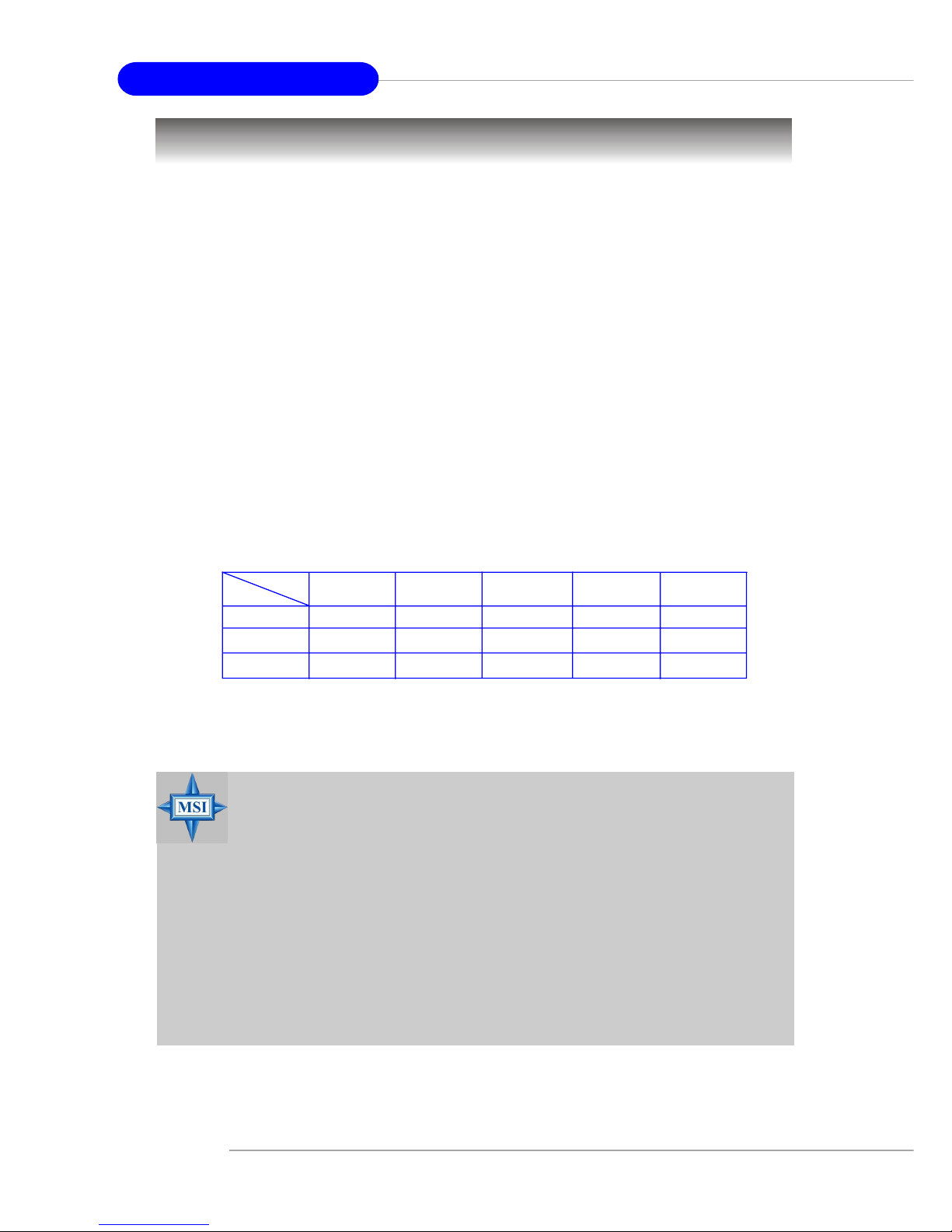
CPU Core Speed Derivation Procedure
If CPU Clock = 200MHz
Core/Bus ratio = 12
then CPU core speed = Host Clock x Core/Bus ratio
= 200MHz x 12
= 2.4 GHz
MSI Reminds You...
Overheating
Overheating will seriously damage the CPU and system, always make sure
the cooling fan can work properly to protect the CPU from overheating.
Overclocking
This motherboard is designed to support overclocking. However, please
make sure your components are able to tolerate such abnormal settings
while doing overclocking. Any attempt to operate beyond product
specifications is not recommended. We do not guarantee the damages
or risks caused by inadequate operation or beyond product
specifications.
DDR266 DDR333 DDR400 DDR433 DDR466
FSB400 OK N/A N/A N/A N/A
FSB533 OK OK N/A N/A N/A
FSB800 OK OK OK OK* OK*
FSB
Memory
Memory Speed/CPU FSB Support Matrix
Note:
1. *: Overclocking specifications
2. FSB800 applies to PT880/PT800 only
Page 15
2-3
Hardware Setup
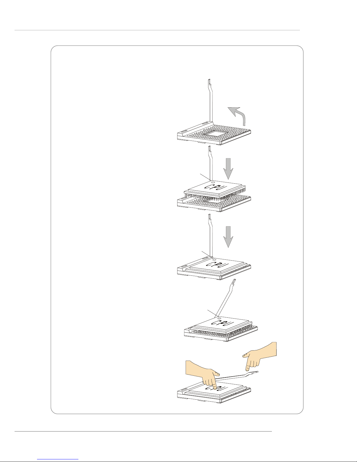
CPU Installation Procedures for Socket 478
1. Please turn off the power and
unplug the power cord before
installing the CPU.
2. Pull the lever sideways away
from the socket. Make sure to
raise the lever up to a 90-degree angle.
3. Look for the gold arrow. The gold
arrow should point towards the
lever pivot. The CPU can only fit
in the correct orientation.
4. If the CPU is correctly installed,
the pins should be completely
embedded into the socket and
can not be seen. Please note
that any violation of the correct
installation procedures may
cause permanent damages to
your mainboard.
5. Press the CPU down firmly into
the socket and close the lever.
As the CPU is likely to move while
the lever is being closed, always close the lever with your
fingers pressing tightly on top of
the CPU to make sure the CPU is
properly and completely embedded into the socket.
Open Lever
90 degree
Sliding
Plate
Close
Lever
Press down
the CPU
Gold arrow
Gold arrow
Gold arrow
Correct CPU placement
Incorrect CPU place me n t
X
O
Page 16
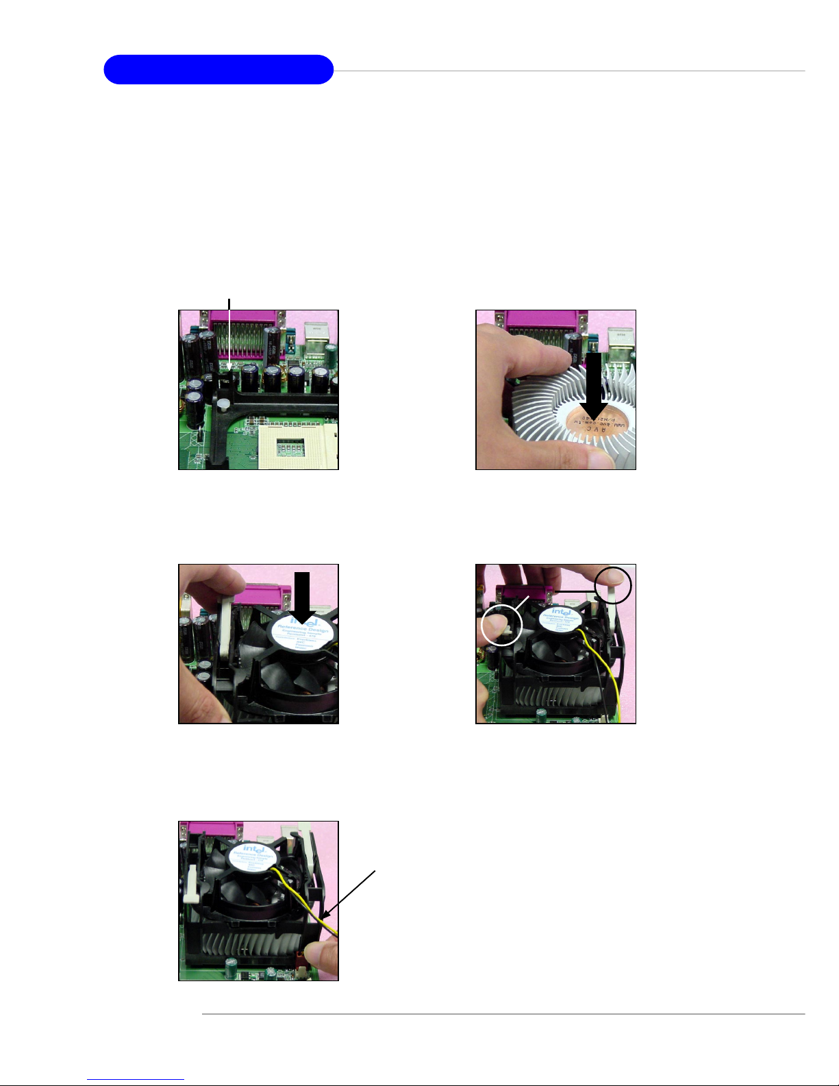
2-4
MS-7043 ATX Mainboard
5. Connect the fan power cable from
the mounted fan to the 3-pin fan
power connector on the board.
Installing the CPU Fan
As processor technology pushes to faster speeds and higher performance,
thermal management becomes increasingly important. To dissipate heat, you need to
attach the CPU cooling fan and heatsink on top of the CPU. Follow the instructions
below to install the Heatsink/Fan:
2. Position the heatsink onto the retention mechanism.
1. Locate the CPU and its retention
mechanism on the motherboard.
3. Mount the fan on top of the heatsink.
Press down the fan until its four clips
get wedged in the holes of the retention mechanism.
4. Press the two levers down to fasten
the fan. Each lever can be pressed
down in only ONE direction.
retention mechanism
levers
fan power cable
Page 17
2-5
Hardware Setup
Memory
Memory Population Rules
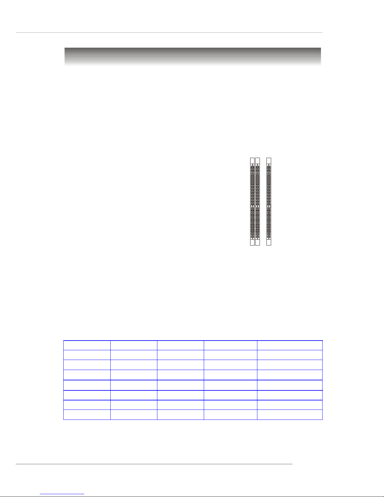
Install at least one DIMM module on the slots. Each DIMM slot supports up to a
maximum size of 1GB. You can install either single- or double-sided modules to meet
your own needs.
The PT880 Neo-V supports dual-channel mode and the PT8 Neo-V & PX8 NeoV support only single-channel mode. Users may install memory modules of different
types and density under single-channel mode. Under dual-channel mode, however,
please make sure that you install memory modules of the same type and density
on DDR DIMMs “in pairs” -- {DIMM1 & DIMM3} or {DIMM2 & DIMM3} to ensure
system stability.
The PT880 Neo-V provides 3 slots for 184-pin, 2.5V DDR DIMM and supports
up to 3GB memory size. You can install DDR266/DDR333/DDR400/DDR433/DDR466
SDRAM modules on the DDR DIMM slots (DIMM 1~3).
The PT8 Neo-V & PX8 Neo-V provide 2 slots for 184-pin, 2.5V DDR DIMM and
supports up to 2GB memory size. You can install DDR266 / DDR333 / DDR400 (for
PT8 Neo-V only) / DDR433 (for PT8 Neo-V only)/DDR466 (for PT8 Neo-V only)
SDRAM modules on the DDR DIMM slots (DIMM 1~2).
To operate properly, at least one DIMM module must be installed. Please note
that DDR433/DDR466 are overclocking specs for PT880 Neo-V/PT8 Neo-V
only.
DDR DIMM Slots
(DIMM 1~3, from left to right)
Channel A: DIMM1 & DIMM2 (green)
Channel B: DIMM3 (purple, for PT880 only)
Memory modules can be installed in any combination as follows:
Please refer to http://www.msi.com.tw/program/products/mainboard/
mbd/pro_mbd_trp_list.php for compatible DDR modules.
S: Single-Channel Mode D: Dual-Channel Mode
DIMM1 DIMM2 DIMM3 System Density Mode
128MB~1GB 128MB~1GB S
128MB~1GB 128MB~1GB S
128MB~1GB 128MB~1GB S (for PT880 only)
128MB~1GB 128MB~1GB 256MB~2GB S
128MB~1GB 128MB~1GB 256MB~2GB D (for PT880 only)
128MB~1GB 128MB~1GB 256MB~2GB D (for PT880 only)
128MB~1GB 128MB~1GB 128MB~1GB 384MB~3GB S (for PT880 only)
Page 18
2-6
MS-7043 ATX Mainboard
Power Supply
The mainboard supports ATX power supply for the power system. Before
inserting the power supply connector, always make sure that all components are
installed properly to ensure that no damage will be caused.
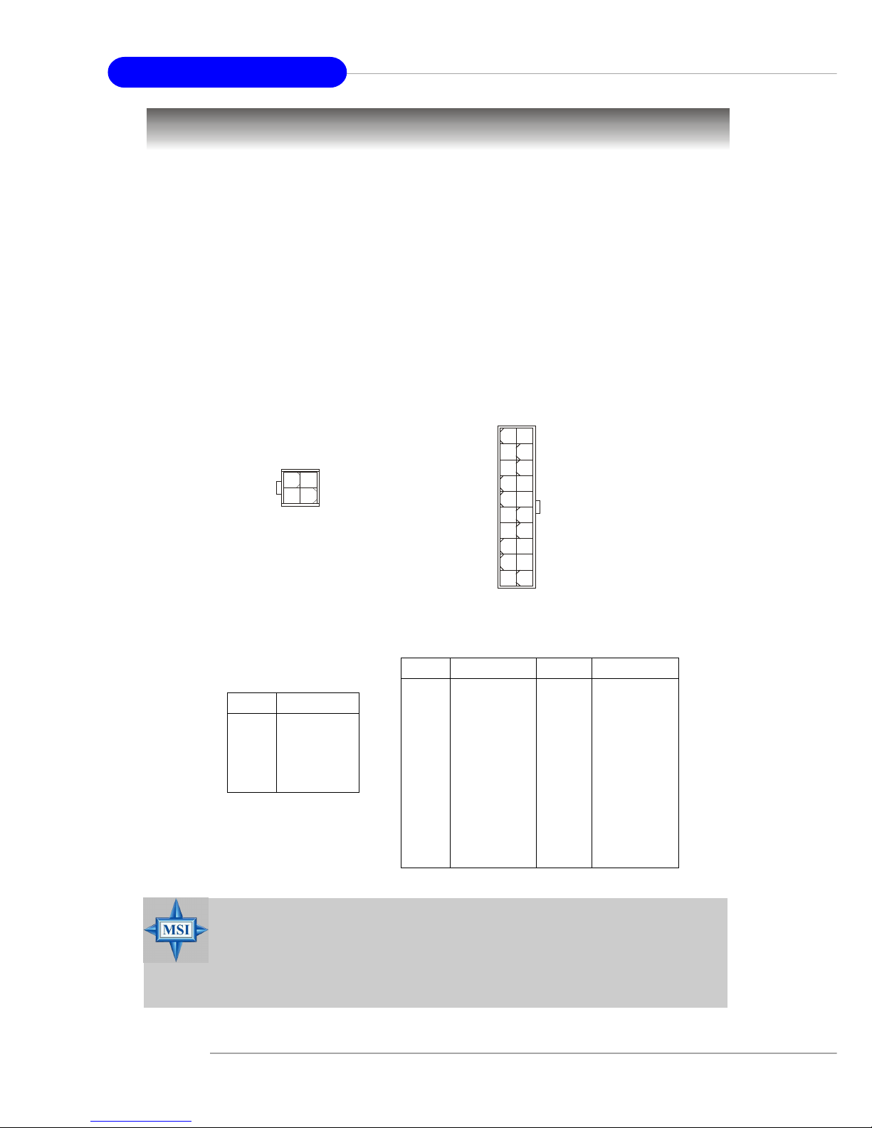
ATX 20-Pin Power Connector: A TX 1
This connector allows you to connect to an ATX power supply. To connect to
the ATX power supply, make sure the plug of the power supply is inserted in the
proper orientation and the pins are aligned. Then push down the power supply firmly
into the connector.
ATX 12V Power Connector: JPW1
This 12V power connector is used to provide power to the CPU.
MSI Reminds You...
1. Power supplies of 300watt (and up) are highly recommended for system stability.
2. Please refer to the Intel/AMD websites for recommended power
supplies.
JPW1 Pin Definition
PIN SIGNAL
1 GND
2 GND
312V
412V
ATX1 Pin Definition
PIN SIGNAL
11 3.3V
12 -12V
13 GND
14 PS_ON
15 GND
16 GND
17 GND
1 8 -5V
19 5V
20 5V
PIN SIGNAL
1 3.3V
2 3.3V
3 GND
45V
5 GND
65V
7 GND
8 PW_OK
9 5V_SB
10 12V
ATX1
10
1
20
11
JPW1
13
42
Page 19
2-7
Hardware Setup
The mainboard provides connectors to connect to FDD, IDE HDD, case, USB
Ports and CPU/System/Power Supply FAN.
Connectors
FDD1
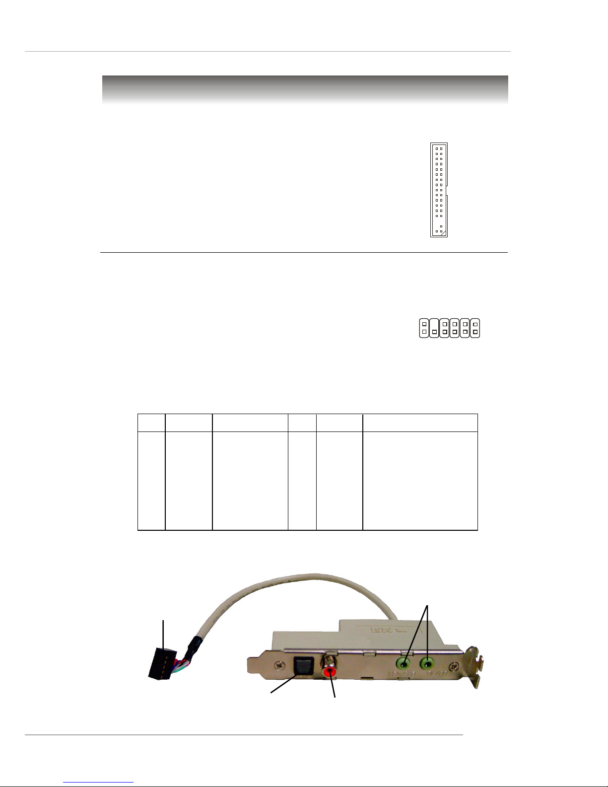
Floppy Disk Drive Connector: FDD1
The mainboard provides a standard floppy disk drive
connector that supports 360K, 720K, 1.2M, 1.44M and 2.88M
floppy disk types.
S-Bracket (SPDIF) Connector: JSP1 (Optional)
The connector allows you to connect a S-Bracket for Sony & Philips Digital
Interface (SPDIF). The S-Bracket offers 2 SPDIF jacks for
digital audio transmission (one for optical fiber connection
and the other for coaxial), and 2 analog Line-Out jacks for 4channel audio output.
To attach the fiber-optic cable to optical SPDIF jack, you
need to remove the plug from the jack first. The two SPDIF jacks support SPDIF
output only.
PIN SIGNAL DESCRIPTION PIN SIGNAL DESCRIPTION
1 VCC5 VCC 5V 2 VDD3 VDD 3.3V
3 SPDFO S/PDIF output 4 (No Pin) Key
5 GND Ground 6 SPDFI S/PDIF input
7 LFE-OUT Audio bass output 8 SOUT-R Audio right surrounding output
9 CET-OUT Audio center output 1 0 SOUT-L Audio left surrounding output
11 GND Ground 12 GND Ground
JSP1 Pin Definition
JSP1
1 11
12 2
Optional S-Bracket
SPDIF jack (optical)
SPDIF jack (coaxial)
Analog Line-Out
Connect to JSP1
Page 20
2-8
MS-7043 ATX Mainboard
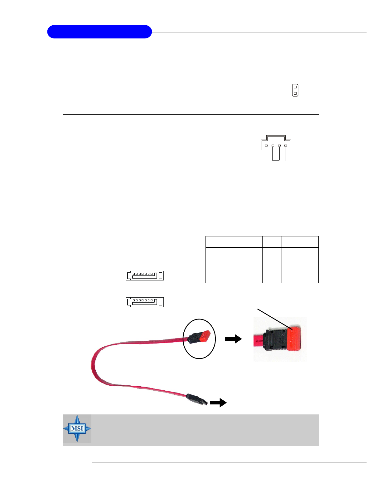
Serial ATA RAID 0, 1 Connectors: SATA1, SATA2 (for PT880/PT8
Neo-V)
The southbridge VIA® VT8237 provides a hybrid solution that combines two
independent SATA ports for support of up to two Serial ATA (Serial ATA RAID) drives
and supports RAID levels 0 or 1 for easy
management of the storage subsystems. Both
connectors support 1st generation serial ATA
data rate of 150 MB/s and are fully compliant
with Serial ATA 1.0 specifications.
PIN SIGNAL PIN SIGNAL
1 GND 2 TXP
3 TXN 4 GND
5 RXN 6 RXP
7 GND
SATA1/2 Pin Definition
SATA2
SATA1
7
1
7
1
MSI Reminds You...
Please do not fold the Serial ATA cable into 90-degree angle. Otherwise,
data loss may occur during transmission.
Connect to SATA1 or SA TA2
Take out the dust cover and connect
to the hard disk devices
Optional Serial A TA cable
Chassis Intrusion Switch Connector: JCI1 (Optional)
This connector is connected to a 2-pin chassis switch. If the chassis is opened,
the switch will be short. The system will record this status and
show a warning message on the screen. To clear the warning, you
must enter the BIOS utility and clear the record.
JCI1
2
1
GND
CINTRU
JCD1
GND L
R
CD-In Connector: JCD1
The connector is for CD-ROM audio connector.
Page 21
2-9
Hardware Setup
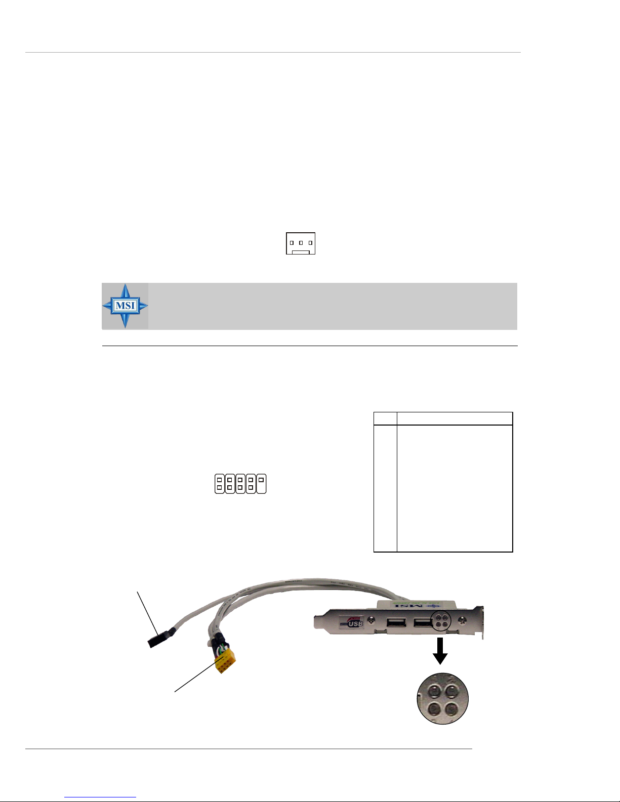
D-Bracket™ 2 Connector: JDB1 (Optional)
The mainboard comes with a JDB1 connector for you to connect to D-Bracket™
2. D-Bracket™ 2 is a USB Bracket that supports both
USB1.1 & 2.0 spec. It integrates four LEDs and allows
users to identify system problems through 16 various
combinations of LED signals.
Pin Signal
1 DBG1 (high for green color)
2 DBR1 (high for red color)
3 DBG2 (high for green color)
4 DBR2 (high for red color)
5 DBG3 (high for green color)
6 DBR3 (high for red color)
7 DBG4 (high for green color)
8 DBR4 (high for red color)
9 Key
10 NC
JDB1 Pin Definition
JDB1
1
9
2
10
D-Bracket™ 2
(Optional)
Connect to JDB1
LEDs
Connect to JUSB1/JUSB2
Fan Power Connector: CPUFA1
The CPUFA1 (processor fan) supports system cooling fan with +12V. It supports three-pin head connector. When connecting the wire to the connectors, always take note that the red wire is the positive and should be connected to the +12V,
the black wire is Ground and should be connected to GND. If the mainboard has a
System Hardware Monitor chipset onboard, you must use a specially designed fan
with speed sensor to take advantage of the CPU fan control.
CPUFA1
Sensor
+12V
GND
MSI Reminds You...
Always consult the vendors for proper CPU cooling fans.
Page 22
2-10
MS-7043 ATX Mainboard
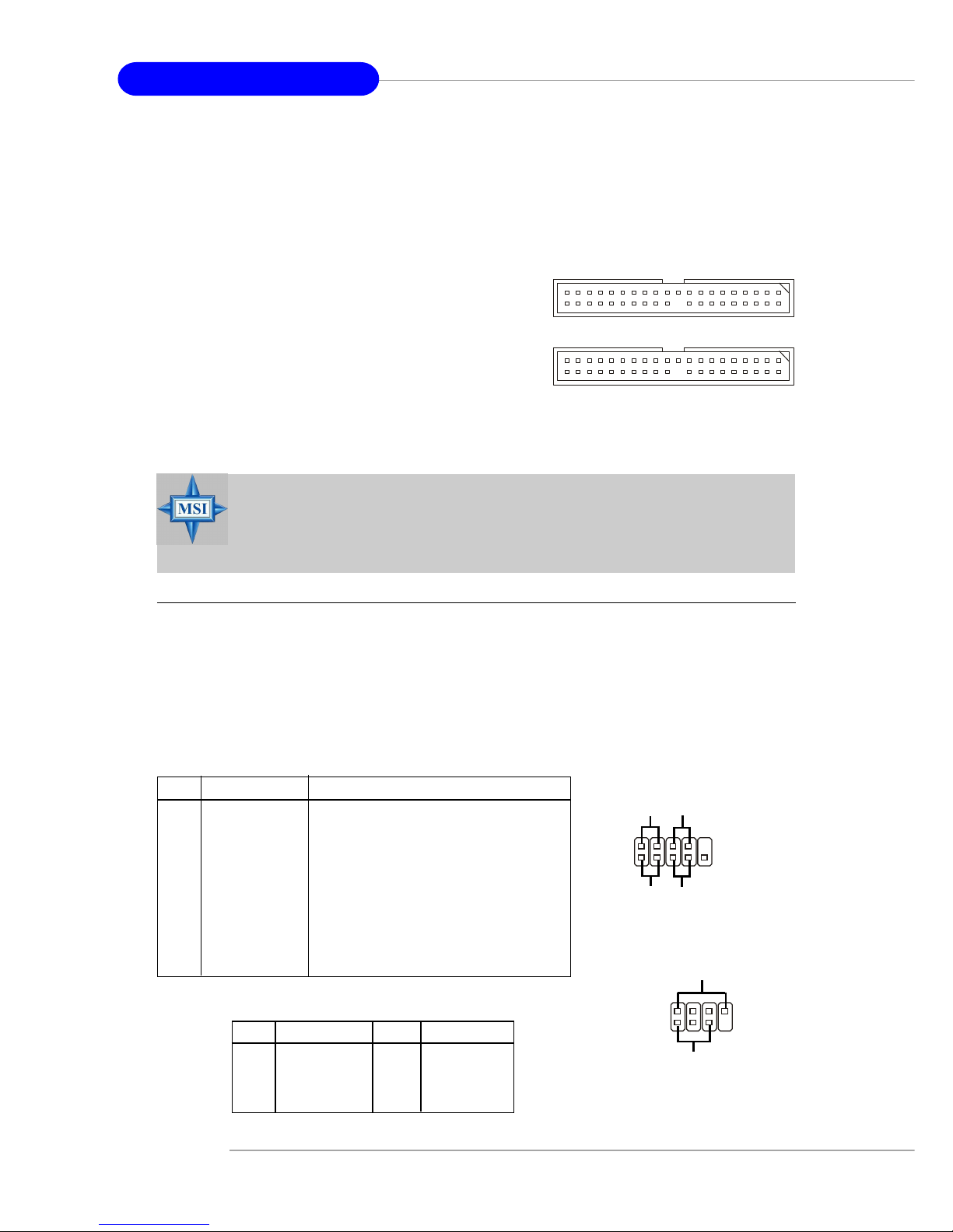
Hard Disk Connectors: IDE1 & IDE2
The mainboard has a 32-bit Enhanced PCI IDE and Ultra DMA 33/66/100/133
controller that provides PIO mode 0~4, Bus Master, and Ultra DMA 33/66/100/133
function. You can connect up to four hard disk drives, CD-ROM, 120MB Floppy and
other devices.
IDE1 (Primary IDE Connector)
The first hard drive should always be
connected to IDE1. IDE1 can connect a Master
and a Slave drive. Y ou must configure second
hard drive to Slave mode by setting the jumper
accordingly.
IDE2 (Secondary IDE Connector)
IDE2 can also connect a Master and a Slave drive.
MSI Reminds You...
If you install two hard disks on cable, you must configure the second drive
to Slave mode by setting its jumper. Refer to the hard disk documentation
supplied by hard disk vendors for jumper setting instructions.
PIN SIGNAL DESCRIPTION
1 HD_LED_P Hard disk LED pull-up
2 FP PWR/SLP MSG LED pull-up
3 HD_LED_N Hard disk active LED
4 FP PWR/SLP MSG LED pull-up
5 RST_SW_N Reset Switch low reference pull-down to GND
6 PWR_SW_P Power Switch high reference pull-up
7 RST_SW_P Reset Switch high reference pull-up
8 PWR_SW_N Power Switch low reference pull-down to GND
9 RSVD_DNU Reserved. Do not use.
JFP1 Pin Definition
PIN SIGNAL PIN SIGNAL
1 GND 2 SPK3 SLED 4 BUZ+
5 PLED 6 BUZ7 NC 8 SPK+
JFP2 Pin Definition
IDE1
IDE2
Front Panel Connectors: JFP1 & JFP2
The mainboard provides two front panel connectors for electrical connection
to the front panel switches and LEDs. The JFP1 is compliant with Intel® Front Panel I/
O Connectivity Design Guide.
Power
LED
Speaker
1
2
7
8
JFP2
9
1
2
10
JFP1
HDD
LED
Reset
Switch
Power
LED
Power
Switch
Page 23
2-11
Hardware Setup
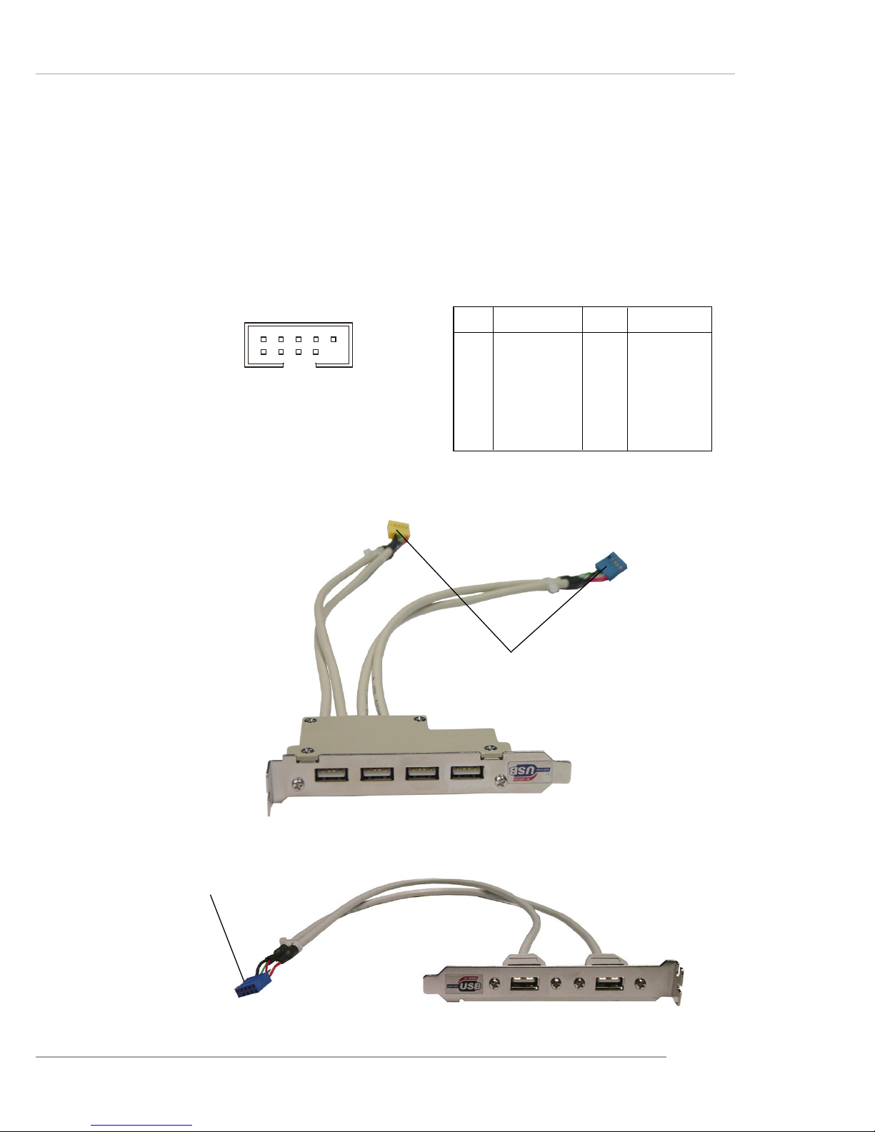
Front USB Connectors: JUSB1 & JUSB2 (Optional)
The mainboard provides two USB 2.0 pin headers JUSB1 & JUSB2 (Optional)
that are compliant with Intel® I/O Connectivity Design Guide. USB 2.0 technology
increases data transfer rate up to a maximum throughput of 480Mbps, which is 40
times faster than USB 1.1, and is ideal for connecting high-speed USB interface
peripherals such as USB HDD, digital cameras, MP3 players, printers, modems
and the like.
PIN SIGNAL PIN SIGNAL
1 VCC 2 VCC
3 USB0- 4 USB15 USB0+ 6 USB1+
7 GND 8 GND
9 Key (no pin) 1 0 USBOC
JUSB1 & JUSB2 Pin Definition
JUSB1/ JUSB2
(USB 2.0/Intel spec)
1
2
9
10
Connect to JUSB1/JUSB2
2-Port USB 2.0 Bracket (Optional)
Connect to JUSB1 & JUSB2 separately
4-Port USB 2.0 Bracket (Optional)
Page 24
2-12
MS-7043 ATX Mainboard
The motherboard provides the following jumpers for you to set the computer’s
function. This section will explain how to change your motherboard’s function through
the use of jumpers.
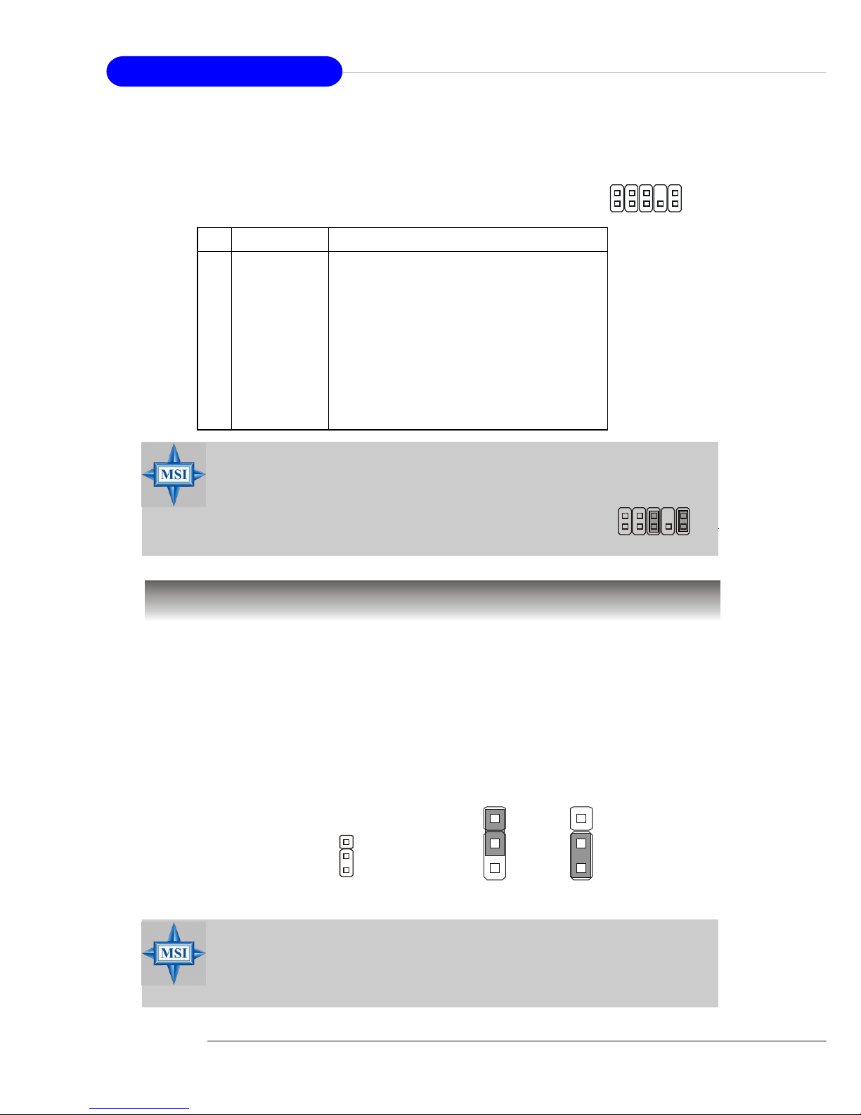
Clear CMOS Jumper: JBA T1
There is a CMOS RAM on board that has a power supply from external battery
to keep the data of system configuration. With the CMOS RAM, the system can
automatically boot OS every time it is turned on. If you want to clear the system
configuration, use the JBAT1 (Clear CMOS Jumper ) to clear data. Follow the instructions below to clear the data:
Jumpers
JBAT1
1
MSI Reminds You...
You can clear CMOS by shorting 2-3 pin while the system is off. Then
return to 1-2 pin position. Avoid clearing the CMOS while the system
is on; it will damage the mainboard.
Clear Data
1
3
Keep Data
1
3
Front Panel Audio Connector: JAUD1
The JAUD1 front panel audio connector allows you to connect to the front
panel audio and is compliant with Intel® Front Panel I/O Connectivity Design Guide.
JAUD1
1
2
9
10
PIN SIGNAL DESCRIPTION
1 AUD_MIC Front panel microphone input signal
2 AUD_GND Ground used by analog audio circuits
3 AUD_MIC_BIAS Microphone power
4 AUD_VCC Filtered +5V used by analog audio circuits
5 AUD_FPOUT_R Right channel audio signal to front panel
6 AUD_RET_R Right channel audio signal return from front panel
7 HP_ON Reserved for future use to control headphone amplifier
8 KE Y No pin
9 AUD_FPOUT_L Left channel audio signal to front panel
1 0 AUD_RET_L Left channel audio signal return from front panel
JAUD1 Pin Definition
MSI Reminds You...
If you don’t want to connect to the front audio header, pins 5 & 6, 9 &
10 have to be jumpered in order to have signal output
directed to the rear audio ports. Otherwise, the Line-Out
connector on the back panel will not function.
5
6
10
9
Page 25
2-13
Hardware Setup
Slots
PCI Interrupt Request Routing
The IRQ, acronym of interrupt request line and pronounced I-R-Q, are hardware lines over which devices can send interrupt signals to the microprocessor. The
PCI IRQ pins are typically connected to the PCI bus INT A# ~ INT D# pins as follows:
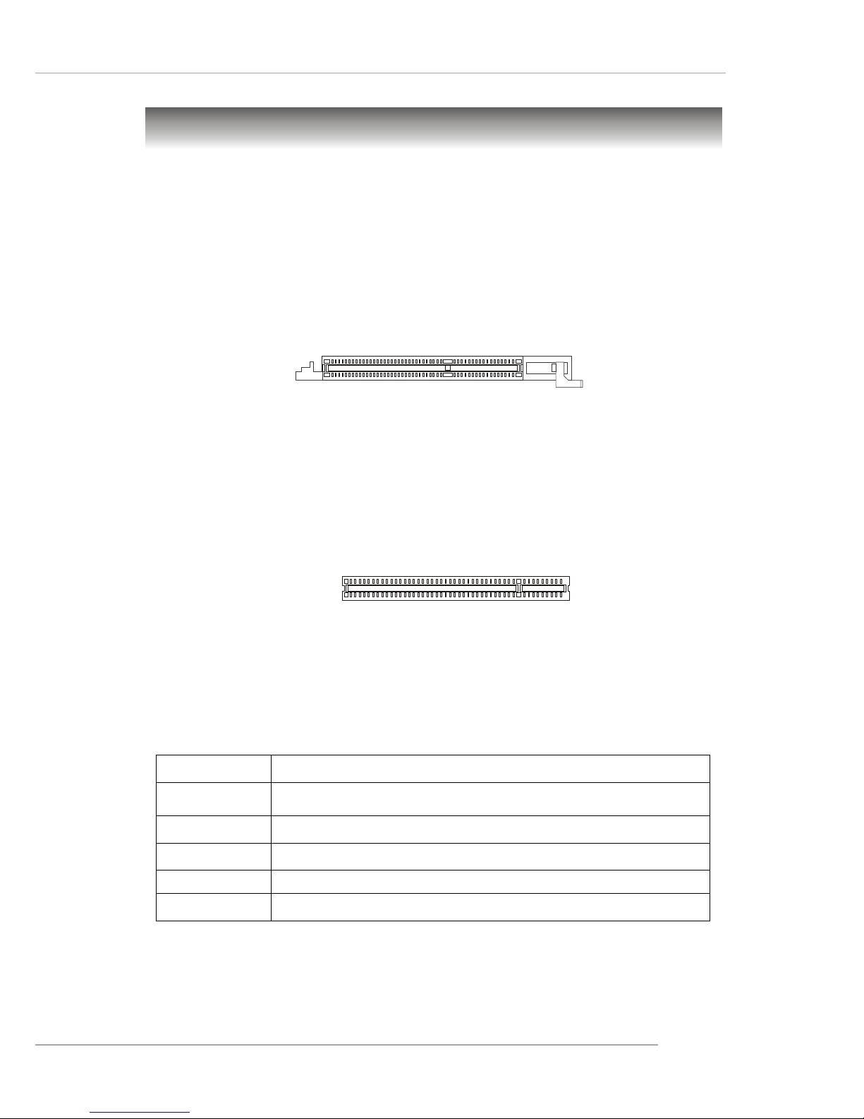
AGP (Accelerated Graphics Port) Slot
The AGP slot allows you to insert the AGP graphics card. AGP is an interface
specification designed for the throughput demands of 3D graphics. It introduces a
66MHz, 32-bit channel for the graphics controller to directly access main memory.
The slot supports 8x/4x AGP card.
PCI (Peripheral Component Interconnect) Slots
The PCI slots allow you to insert the expansion cards to meet your needs.
When adding or removing expansion cards, make sure that you unplug the power
supply first. Meanwhile, read the documentation for the expansion card to make any
necessary hardware or software settings for the expansion card, such as jumpers,
switches or BIOS configuration.
The mainboard provides one AGP slot and five 32-bit PCI bus slots.
Order 1 Order 2 Order 3 Order 4
PCI Slot 1 INT A# INT B# INT C# INT D#
PCI Slot 2 INT B# INT C# INT D# INT A#
PCI Slot 3 INT C# INT D# INT A# INT B#
PCI Slot 4 IN T D # INT A# INT B# INT C#
PCI Slot 5 INT B# INT C# INT D# INT A#
AGP Slot
PCI Slot
Page 26

3-1
BIOS Setup
Chapter 3. BIOS Setup
This chapter provides Frequency/Voltage Control information
on the BIOS Setup program and allows you to configure the system
for optimum use. You may need to run the Setup program when:
An error message appears on the screen during the system boot-
ing up, and requests you to run SETUP.
You want to change the default settings for customized features.
Upon boot-up, the 1st line appearing after the memory count is
the BIOS version. It is usually in the format:
A6380MS V1.0 091096 where:
1st digit refers to BIOS maker as A = AMI(R) W = AWARD(R).
2nd - 5th digit refers to the model number.
6th - 7th digit refers to the customer as MS = all standard customers.
V1.0 refers to the BIOS version.
091096 refers to the date this BIOS was released.
For detailed BIOS setup information, please refer to our website
at: http://www.msi.com.tw.
BIOS Setup
Page 27
3-2
MS-7043 ATX Mainboard
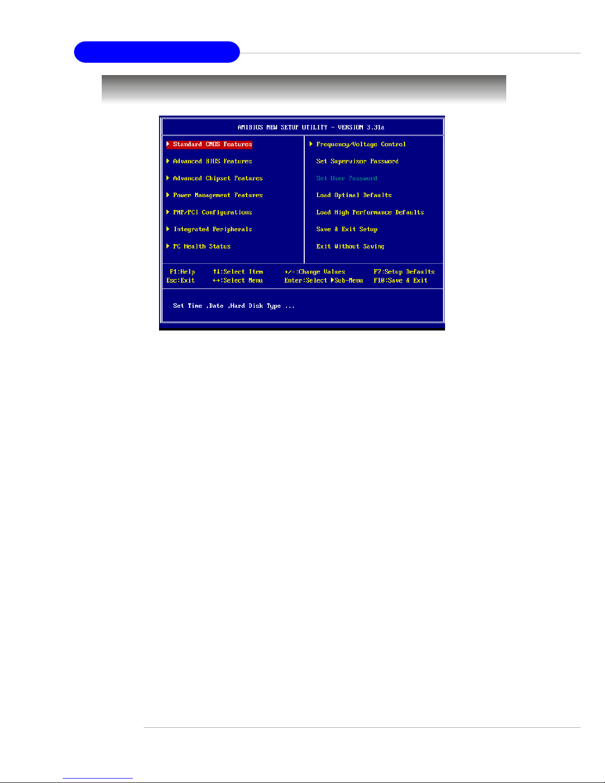
The Main Menu
Standard CMOS Features
Use this menu for basic system configurations, such as time, date etc.
Advanced BIOS Features
Use this menu to setup the items of AMI® special enhanced features.
Advanced Chipset Features
Use this menu to change the values in the chipset registers and optimize your system’s
performance.
Power Management Features
Use this menu to specify your settings for power management.
PNP/PCI Configurations
This entry appears if your system supports PnP/PCI.
Integrated Peripherals
Use this menu to specify your settings for integrated peripherals.
PC Health Status
This entry shows your PC health status.
Frequency/Voltage Control
Use this menu to specify your settings for frequency/voltage control.
Load Optimal Defaults
Use this menu to load the factory default settings for optimal & stable system performance.
Load High Performance Defaults
Use this menu to load the BIOS values for the best system performance, but the system
stability may be affected.
Page 28
3-3
BIOS Setup
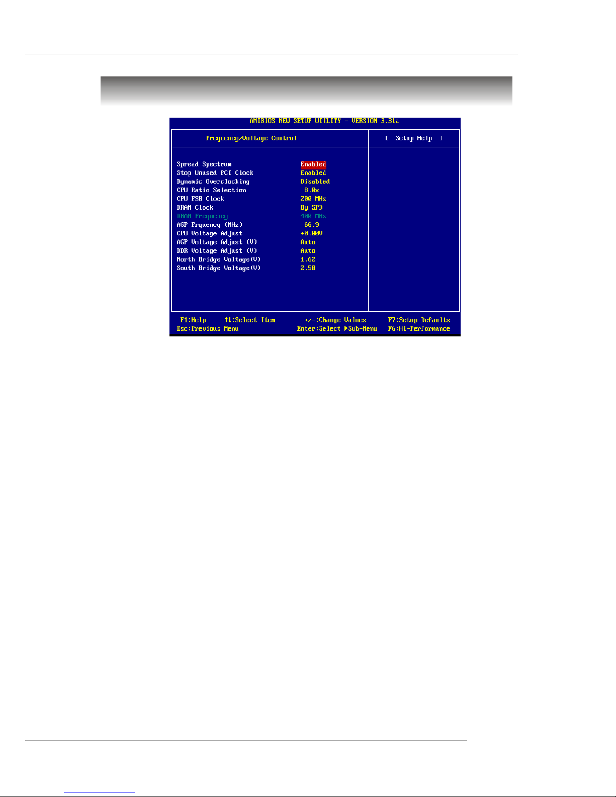
Spread Spectrum
When the motherboard’s clock generator pulses, the extreme values (spikes) of the
pulses creates EMI (Electromagnetic Interference). The Spread Spectrum function
reduces the EMI generated by modulating the pulses so that the spikes of the pulses
are reduced to flatter curves. If you do not have any EMI problem, leave the setting at
[Disabled] for optimal system stability and performance. But if you are plagued by EMI,
set to [Enabled] for EMI reduction. Remember to disable Spread Spectrum if you are
overclocking because even a slight jitter can introduce a temporary boost in clock
speed which may just cause your overclocked processor to lock up.
Stop Unused PCI Clock
This item enables or disables the PCI slot clock. Setting options: [Enabled], [Disabled].
Dynamic Overclocking
Dynamic Overclocking Technology is the automatic overclocking function, included in
the MSITM newly developed CoreCell
TM
Technology. It is designed to detect the load
balance of CPU while running programs, and to adjust the best CPU frequency
automatically. When the motherboard detects that the CPU is running programs, it will
speed up CPU automatically to make the program run smoothly and faster. When the
CPU is temporarily suspending or staying in the low load balance, it will restore the
default settings instead. Usually the Dynamic Overclocking Technology will be powered
only when users' PC need to run huge amount of data like 3D games or the video
process, and the CPU frequency needs to be boosted up to enhance the overall
performance. Setting options:
[Disabled] Disable Dynamic Overclocking.
[Private] 1st level of overclocking.
[Sergeant] 2nd level of overclocking.
[Captain] 3rd level of overclocking, also the default value of "Load
High Performance Defaults".
Frequency/Voltage Control
Page 29
3-4
MS-7043 ATX Mainboard
[Colonel] 4th level of overclocking.
[General] 5th level of overclocking.
[Commander] 6th level of overclocking.
CPU Ratio Selection
This setting controls the multiplier that is used to determine the internal clock speed of
the processor relative to the external or motherboard clock speed.
CPU FSB Clock
This setting shows the current CPU Front Side Bus clock frequency.
DRAM Clock
Use this field to configure the clock frequency of the installed DRAM. Setting options:
FSB100: [By SPD], [DDR 266 (3:4)], [DDR 333 (3:5)], [DDR 400 (1:2)], [DDR
433], [DDR 450], [DDR 466], [DDR 500]
FSB133: [By SPD], [DDR 266 (1:1)], [DDR 333 (4:5)], [DDR 400 (2:3)], [DDR
433], [DDR 450], [DDR 466], [DDR 500]
FSB200: [By SPD], [DDR 266 (3:2)], [DDR 333 (6:5)], [DDR 400 (1:1)], [DDR
433], [DDR 450], [DDR 466], [DDR 500]
DRAM Frequency
This setting shows the current frequency of DDR DRAM (read only).
AGP Frequency (MHz)
This item is used to configure the AGP frequency.
MSI Reminds You...
The value plus a ratio (CPU: DDR) with parentheses means the nonsynchronous overclocking.
MSI Reminds You...
1. Even though the Dynamic Overclocking Technology is more stable
than manual overclocking, basically, it is still risky. We suggest
that users make sure that the CPU can afford to overclocking regularly first. If you find the PC appears to be unstable or reboot
incidentally, it's better to disable the Dynamic Overclocking or to
lower the level of overclocking options. By the way, if you need to
conduct overclocking manually, you also need to disable the Dynamic OverClocking first.
2. Meanwhile, there are two functions to protect user's system from
crashing.
- There is a safe key "Ins" in BIOS. In case the overclocking
fails, you can press "Ins" key while system rebooting to restore to the BIOS defaults.
- If the system incidentally reboot for four times, the BIOS will
also be restored to the defaults.
Page 30

3-5
BIOS Setup
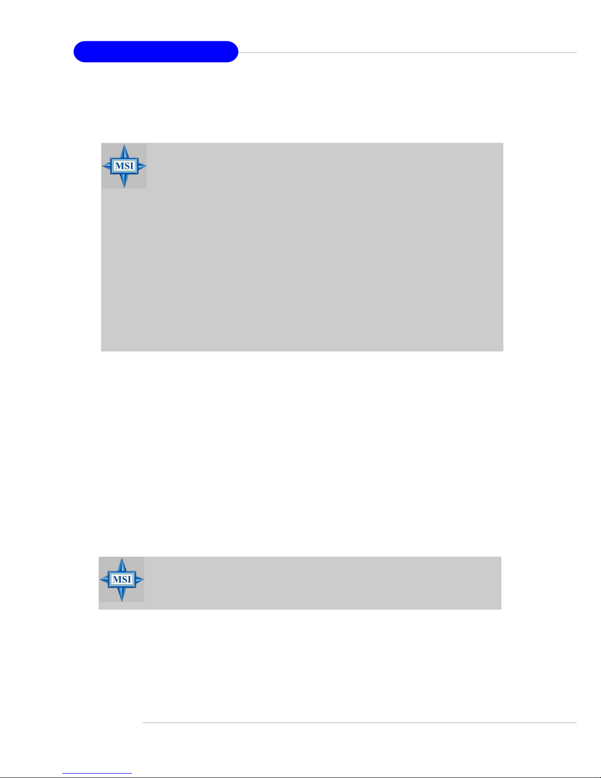
MSI Reminds You...
The settings shown in different color in CPU Voltage, DDR Voltage,
AGP Voltage, and North Bridge/South Bridge Voltage help to verify if
your setting is proper for your system.
White: Safe setting.
Yellow: High performance setting.
Red: Not recommended setting and the system may be unstable.
Changing CPU/DDR/AGP/North Bridge/South Bridge Voltage may re-
sult in the instability of the system; therefore, it is NOT recommended
to change the default settings for long-term usage.
CPU Voltage Adjust
The setting allows you to adjust the CPU Vcore voltage, which depends on the CPU.
AGP Voltage Adjust (V)
AGP voltage is adjustable in the field, allowing you to increase the performance of your
AGP display card when overclocking, but the stability may be affected.
DDR Voltage Adjust (V)
This setting is used to adjust the DRAM core voltage (Vcore), making overclocking
possible.
North Bridge/South Bridge Voltage (V)
These two items configure the voltage of the North Bridge and the South Bridge for
overclocking purposes.
 Loading...