

Page 1
Page 2

CHAPTER 1 INTRODUCTION
1-1
Chapter 1
Introduction
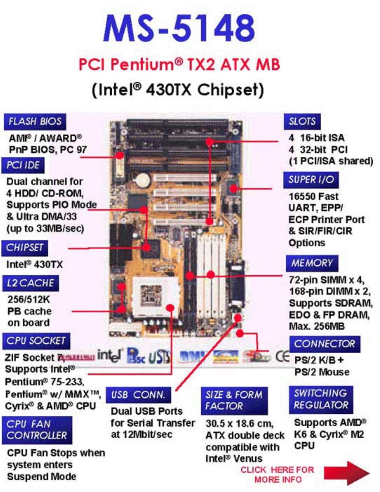
The PCI 430 TX system board is a high-performance personal computer
system board based on a 3.3v version of the PentiumTM micrprocessor--the
P54C and P55C, K6 and M2 with MMX microprocessor . The system board
supports the Peripheral Component Interconnect (PCI) Local Bus Standard
and provide four 32-bit PCI bus master slots.
A cache subsystem can be configured for 256k or 512K cache memory to
improve overall throughput.
The system board uses the highly integrated Intel 82439TX chipset to
support the PCI/ISA and green standards, and to provide the Host/PCI
bridge. The 82437AB chipset also support the ACPI soft power off and
Modem Ring wake-up function, it also integrates all system control functions.
Page 3

CHAPTER 1 INTRODUCTION
1-2
1.1 System Board Features
CPU
l Socket 7 supports Intel Pentium
TM
family -- P54C and P55C((MMX)
90MHz/100MHz/120Mhz/133MHz/150MHz/166MHz/200MHz/233MHz
l The Cyrix 6x86/M2 and AMD K5/K6 are also supported.
Chip Set
l Intel 82430TX
Cache Memory
l Supports Directed Map Organization,W rite-Back cache policy.
l Supports 256K pipelined burst cache memory or 512K pipelined burst
cache memory .
Main Memory
l Supports six memory banks using four 72-pin SIMM sockets and two 168-
pin DIMM sockets.
l Up to 256 Mbytes main memory.
l Supports EDO Hyper Page Mode DRAM , Standard Fast Page mode
DRAM and SDRAM.
Slots
l Four 32-bit Master PCI Bus slots and four 16-bit ISA bus slots. One
shared slot that can be used as ISA or PCI.
l Support 3.3V PCI Add-On Card.
On-Board Peripherals
l On-Board Peripherals include:
- 1 floppy port supports 2FDD
- 2 serial ports (COMA + COMB)
- 1 parallel port supports ECP or EPP mode
- 2 PCI Bus Master IDE ports (up to four IDE HDD)
- 2 Channel USB port
Page 4

CHAPTER 1 INTRODUCTION
1-3
Dimensions
l Standard A TX form factor
l 30cm(L) x 18.6cm(W) x 4 layer PCB
Mounting
l 6 mounting holes
Page 5
CHAPTER 1 INTRODUCTION
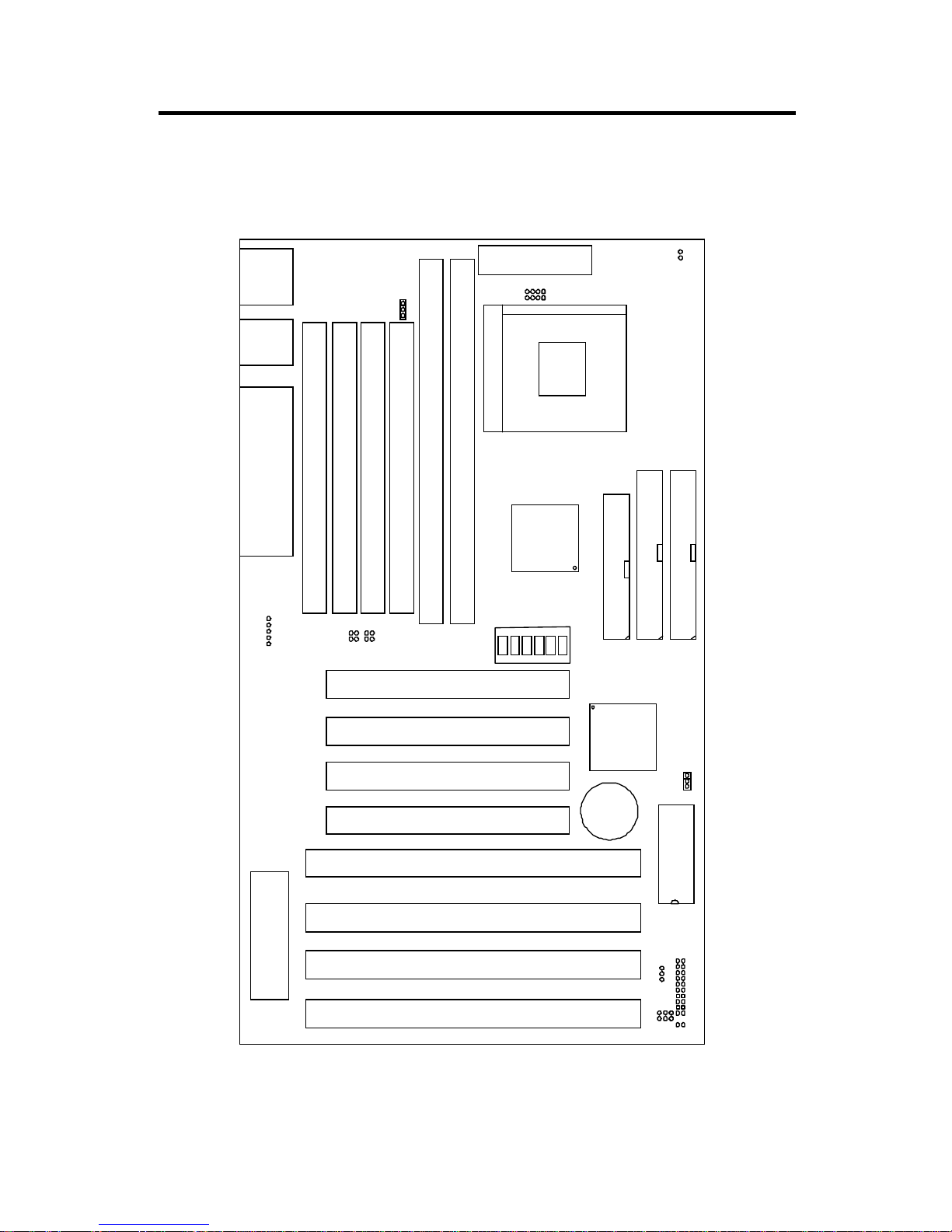
1.3 System Board Layout
MS-5148
SIMM1
SIMM2
SIMM3
SIMM4
DIMM1
DIMM2
Socket 7
FDD
IDE1
IDE2
ISA SLOT 4
ISA SLOT 2
ISA SLOT 3
ISA SLOT 1
PCI SLOT 4
PCI SLOT 3
PCI SLOT 2
PCI SLOT 1
BIOS
BATT
+
2032
JPF
JGS
JGL
JP2
INTEL
FW82371AB
INTEL
FW82439TX
JBAT
JRMS2
JFAN
ATX
POWER CONNECTOR
KBC
IR
JV1
LPT
COMA & COMB
USB
PS/2
JV3
JV4
JV5
SW
ON
DIP
121
3
4
1
5
6
JV6
JRMS1
+
1-4
Page 6
CHAPTER 2 HARDWARE INSTALLATION
CPU
CPU
Open Lever
Pin 1
Sliding
Plate
White dot/
Cut edge
Close
Lever
Chapter 2
Hardware Installation
2.1 Central Processing Unit: CPU
The 430 TX motherboard operates with Intel® P54C/P55C, Cyrix® 6x86/
M2 and AMD ® 5K86/K6 processors. It could operates with 2.8V to 3.52V
processors. The motherboard provides a 321-pin ZIF Socket 7 for easy CPU
installation, a DIP switch (SW1) to set the proper speed for the CPU and a
Jumper block (JV3 - JV7) for setting the CPU voltage. The CPU should
always have a cooling fan attached to prevent overheating.
2-1
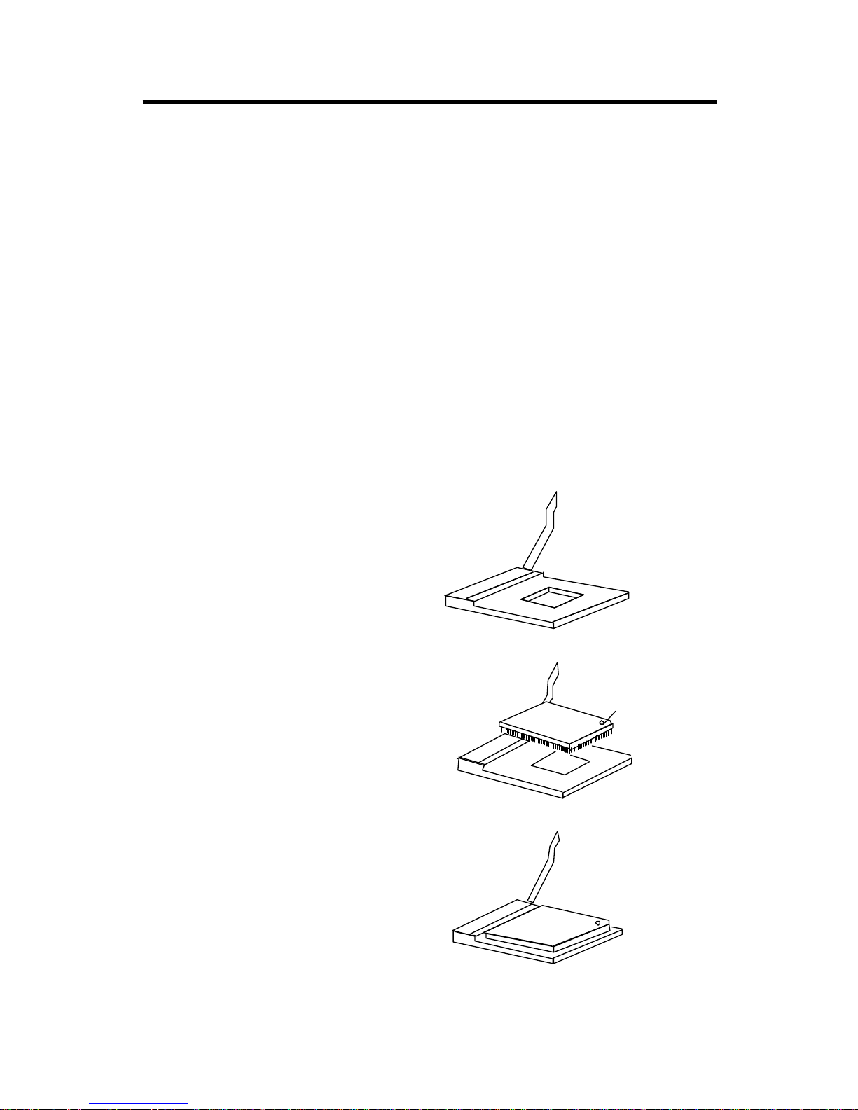
1. Pull the lever sideways away
from the socket then raise
the lever up to a 90-degree
angle.
3. Press the lever down to
complete the installation.
2. Locate Pin 1 in the socket
and look for the white dot or
cut edge in the CPU, match
Pin 1 with the white dot/cut
edge then insert the CPU. It
should insert easily.
2.1-1 CPU Installation Procedure
Page 7

CHAPTER 2 HARDWARE INSTALLATION
1. The 3 CPU clock frequencies that the system supports are 55MHz, 60MHz,
66MHz and 75MHz (To adjust SW1 pin 4, 5, and 6 ). See the following
chart to set the different Host Clock Frequencies.
4 5 6 Clock
ON ON OFF 55MHz
ON OFF OFF 60MHz
OFF OFF OFF 66MHz
OFF ON OFF 75MHz
SW1
CPU
2 . The DIP Switch SW1 (1,2, and 3) is used to set the Core/Bus (Fraction)
ratio of the CPU. The actual core speed of the CPU is the Host Clock
Frequency multiplied by the Core/Bus ratio. For example:
If CPU Clock = 66MHz
Core/Bus ratio = 3 / 2
then CPU core speed = Host Clock x Core/Bus ratio
= 66MHz x 3/2
= 100MHz
3. The PCI Bus Clock is the CPU Clock Frequency divided by 2.
2.1-2 CPU Core Speed Derivation Procedure
1 2 3 Core/Bus Ratio
OFF OFF OFF 1.5 /3.5
ON OFF OFF 2
O N ON OFF 2.5/1.75
OFF ON OFF 3
SW1
CPU
2-2
Page 8
CHAPTER 2 HARDWARE INSTALLATION
2.9
VcoreV I/O
3.38 3.38
3.52
3.52
3.3
2.8
3.3
3.3 3.2
JV3~JV7
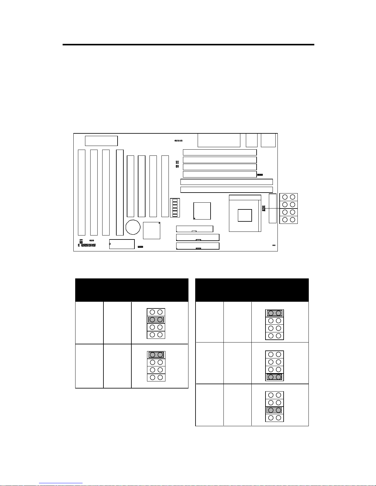
2.1-3 CPU Voltage Setting: JV3 - JV7
The system board can autodetect whether the CPU is single or dual voltage.
T o adjust the Jumper setting of the CPU’s Vcore, just look at table below and
set accordingly.
SIMM1
SIMM2
SIMM3
SIMM4
DIMM1
DIMM2
Socket 7
FDD
IDE1
IDE2
ISA SLOT 4
ISA SLOT 2
ISA SLOT 3
ISA SLOT 1
PCI SLOT 4
PCI SLOT 3
PCI SLOT 2
PCI SLOT 1
BIOS
BATT
+
2032
JPF
JGS
JGL
JP2
INTEL
FW82371AB
INTEL
FW82439TX
JBAT
JRMS2
JFAN
ATX
POWER CONNECTOR
KBC
IR
JV1
LPT
COMA & COMB
USB
PS/2
JV3
JV4
JV5
SW
ON
DIP
121
3
4
1
5
6
JV6
JRMS1
+
JV3
JV4
JV6
JV5
Vcore
V I/O
JV3~JV7
Single Voltage Dual Voltage
2-3
JV3
JV4
JV6
JV5
JV3
JV4
JV6
JV5
JV3
JV4
JV6
JV5
JV3
JV4
JV6
JV5
JV3
JV4
JV6
JV5
Page 9
CHAPTER 2 HARDWARE INSTALLATION
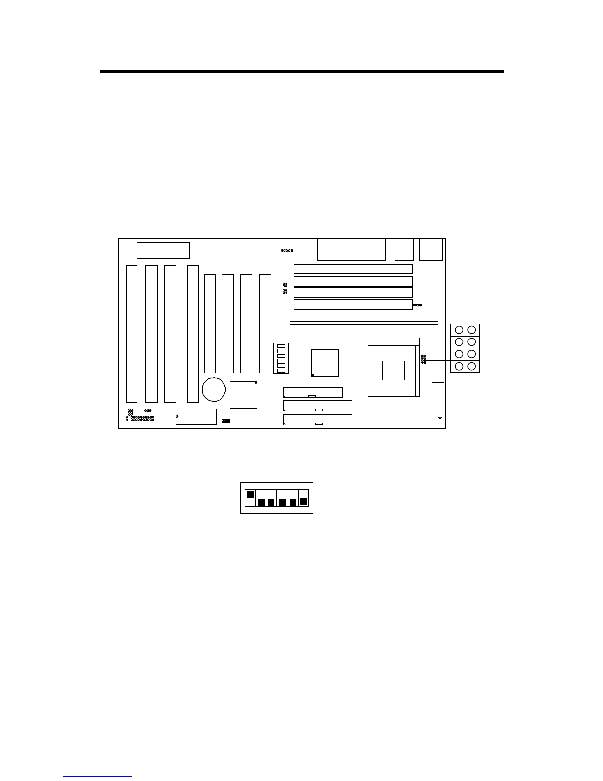
2.1-4 CPU Speed and Voltage Setting: SW1 & JV3-JV7
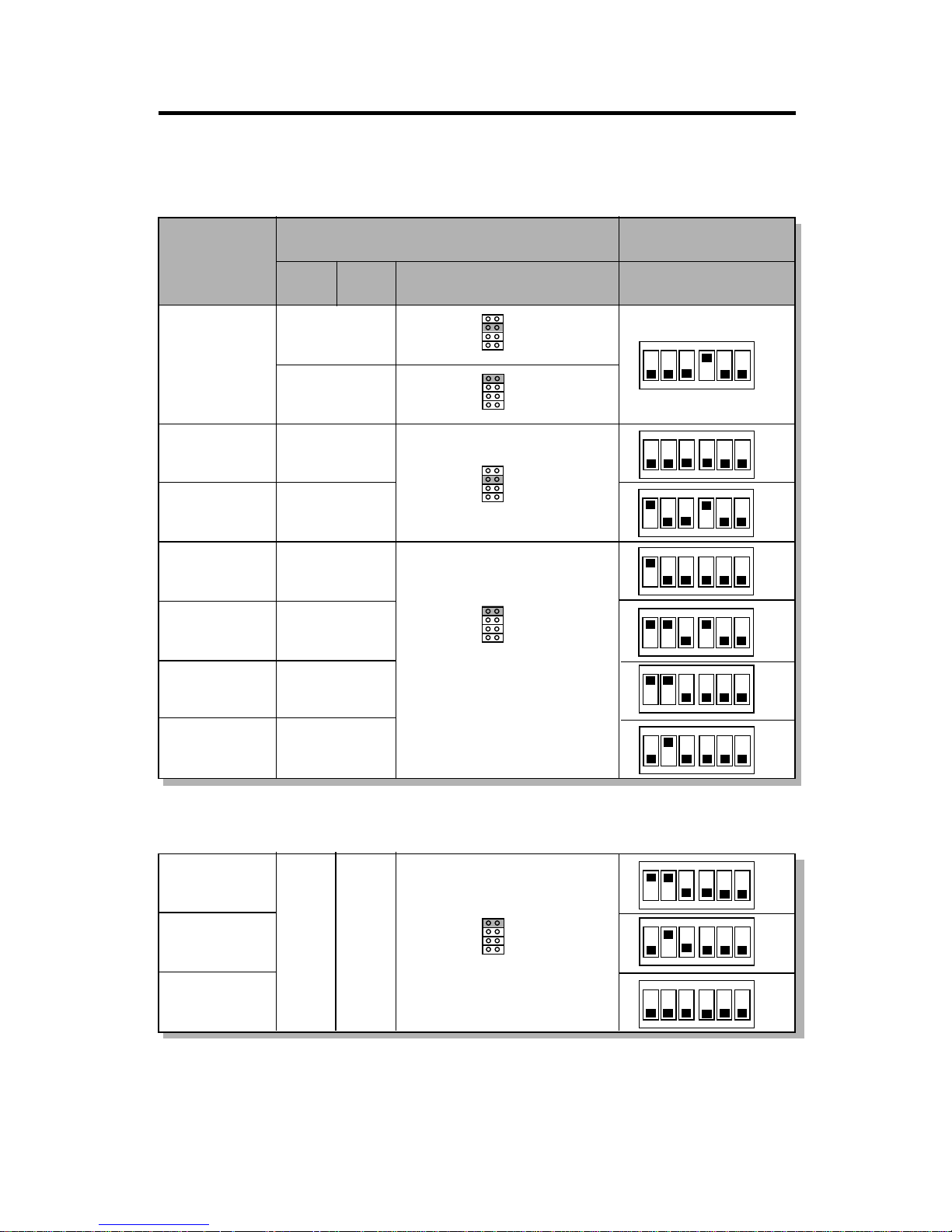
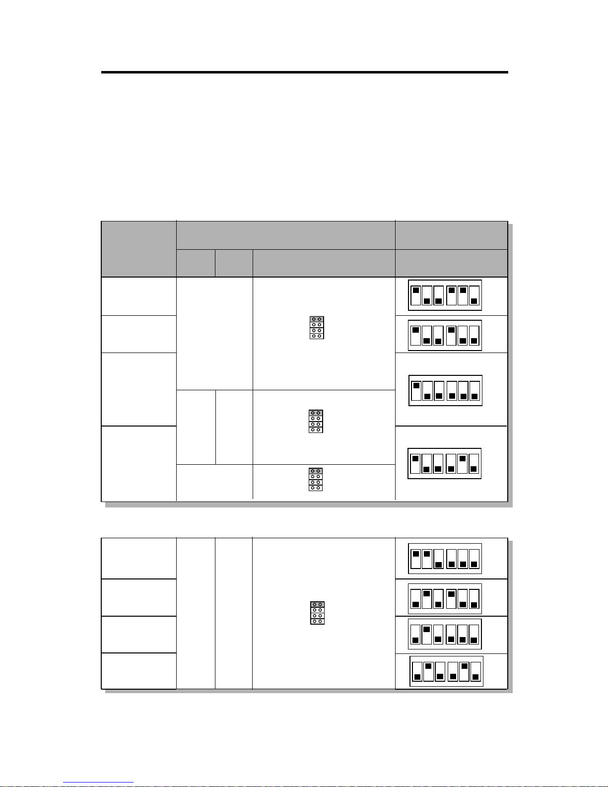
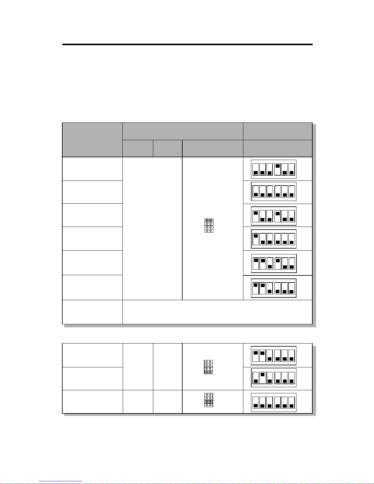
To adjust the speed and voltage of the CPU, you must know the specification of your CPU (always ask the vendor for CPU specificaton) then look at
T able 2.1 (Intel ® P54C/P55C-MMX), Table 2.2 (Cyrix® 6x86/M2) and
T able 2.3 (AMD® 5K86/K6) for proper setting.
SW1
1 2 3 4 5 6
ON
ON
OFF
Speed Setting
2-4
SIMM1
SIMM2
SIMM3
SIMM4
DIMM1
DIMM2
Socket 7
FDD
IDE1
IDE2
ISA SLOT 4
ISA SLOT 2
ISA SLOT 3
ISA SLOT 1
PCI SLOT 4
PCI SLOT 3
PCI SLOT 2
PCI SLOT 1
BIOS
BATT
+
2032
JPF
JGS
JGL
JP2
INTEL
FW82371AB
INTEL
FW82439TX
JBAT
JRMS2
JFAN
ATX
POWER CONNECTOR
KBC
IR
JV1
LPT
COMA & COMB
USB
PS/2
JV3
JV4
JV5
SW
ON
DIP
121
3
4
1
5
6
JV6
JRMS1
+
JV3
JV4
JV6
JV5
Page 10
CHAPTER 2 HARDWARE INSTALLATION
Table 2.1 Intel® P54C PENTIUM CPU
P54C-90
P54C-100
P54C-120
P54C-133
P54C-150
P54C-166
P54C-200
3.38
3.52
3.52
3.38
3.38
3.52
3.52
3.52
ON DIP
123 456
ON
OFF
ON DIP
123 45 6
ON
OFF
ON DIP
123 456
ON
OFF
ON DIP
123 456
ON
OFF
ON DIP
123 456
ON
OFF
CPU Type
CPU SpeedCPU Voltage
SW1VI/O Vcore
ON DIP
123 45 6
ON
OFF
ON DIP
123 456
ON
OFF
2-5
JV3
JV4
JV5
JV6
JV3
JV4
JV5
JV6
JV3
JV4
JV5
JV6
JV3
JV4
JV5
JV6
JV3~JV7
ON DIP
123 456
ON
OFF
ON DIP
123 45 6
ON
OFF
ON DIP
123 456
ON
OFF
P55C-166
P55C-200 3.3 2.8
JV3
JV4
JV5
JV6
P55C-233
Intel® P55C PENTIUM (MMX) CPU
Note: If you encounter a CPU with different Voltage, just go to page 2-3 and
look for the proper voltage settings.
Page 11
CHAPTER 2 HARDWARE INSTALLATION
Table 2.2 Cyrix® 6x86 CPU
Cyrix® 6x86 CPU uses P to rate the speed of there processor base on Intel®
CPU core speed , for example P150+ (120MHz) has 150MHz core speed of
Intel® but has 120MHz core speed in Cyrix®. Cyrix® 6x86 CPU should
always uses a more powerful fan (ask vendor for proper cooling fan).
3.52
ON DIP
123 45 6
ON
OFF
CPU Type
CPU SpeedCPU Voltage
SW1VI/O Vcore
M1 P133+
(1 10MHz)
M1 P150+
(120MHz)
M1 P166+
(133MHz)
ON DIP
123 456
ON
OFF
2-6
M1 P200+
(150MHz)
ON DIP
123 456
ON
OFF
ON DIP
123 456
ON
OFF
3.3 2.8
3.52
JV3
JV4
JV5
JV6
JV3
JV4
JV5
JV6
JV3
JV4
JV5
JV6
JV3~JV7
ON DIP
123 45 6
ON
OFF
M2 P166+
(166MHz)
M2 P180+
(180MHz)
M2 P200+
(200MHz)
ON DIP
123 456
ON
OFF
M2 P225+
(225MHz)
ON DIP
123 456
ON
OFF
3.3 2.8
JV3
JV4
JV5
JV6
ON DIP
123 45 6
ON
OFF
Cyrix® M2 (MMX) CPU
Note: We don’t guarantee the performance of 75MHz Bus Clock.
Page 12
CHAPTER 2 HARDWARE INSTALLATION
Table 2.3 AMD® 5K86 CPU
AMD® 5K86 CPU uses PR to rate the speed of there processor base on
Intel® CPU core speed , for example PR133+ (100MHz) has 133MHz core
speed of Intel® but has 100MHz core speed in AMD® 5K86 CPU.
ON DIP
123 456
ON
OFF
3.52
ON DIP
123 45 6
ON
OFF
123 45 6
CPU Type
CPU SpeedCPU Voltage
SW1
VI/O
Vcore
PR100
(100MHz)
PR120
(90MHz)
ON DIP
123 456
ON
OFF
2-7
PR133
(100MHz)
JV3~JV7
JV3
JV4
JV5
JV6
PR90
(90MHz)
PR150
(105MHz)
PR166
(116.7MHz)
PR200
(133MHz)
Reserved
ON DIP
ON
OFF
ON DIP
ON
OFF
ON DIP
ON
OFF
ON DIP
123 456
ON
OFF
3.3
ON DIP
123 45 6
ON
OFF
PR200
(200MHz)
PR233
(233MHz)
ON DIP
123 456
ON
OFF
JV3
JV4
JV5
JV6
PR166
(166MHz)
2.9
AMD® K6 (MMX) CPU
3.3 3.2
JV3
JV4
JV5
JV6
Note: If you encounter a CPU with different Voltage, just go to page 2-3 and
look for the proper voltage settings.
Page 13
CHAPTER 2 HARDWARE INSTALLATION
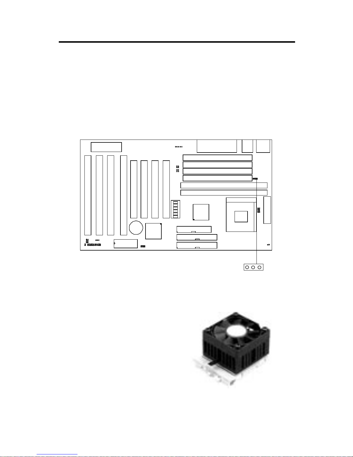
2.1-5 CPU Fan Power Connector: JFAN
This connector supports CPU cooling fan with +12V. It supports both two
and three pin head connector. When connecting the wire to the connector,
always take note that the red wire is the positive and should be connected to
the +12V. If the system is in suspend mode, the fan will stop. You can change
this setup on the Power Management Setup in the BIOS.
JFAN
Connector
+12V
GND
GND
Recommended CPU cooling fan specification:
- Metallic Clip
- RPM 5000
- CFM 10
- +12V
- 52x52x10mm
- Ball Bearing
Note: Always consult vendor for
proper CPU cooling fan.
2-8
SIMM1
SIMM2
SIMM3
SIMM4
DIMM1
DIMM2
Socket 7
FDD
IDE1
IDE2
ISA SLOT 4
ISA SLOT 2
ISA SLOT 3
ISA SLOT 1
PCI SLOT 4
PCI SLOT 3
PCI SLOT 2
PCI SLOT 1
BIOS
BATT
+
2032
JPF
JGS
JGL
JP2
INTEL
FW82371AB
INTEL
FW82439TX
JBAT
JRMS2
JFAN
ATX
POWER CONNECTOR
KBC
IR
JV1
LPT
COMA & COMB
USB
PS/2
JV3
JV4
JV5
SW
ON
DIP
121
3
4
1
5
6
JV6
JRMS1
+
Page 14
CHAPTER 2 HARDWARE INSTALLATION
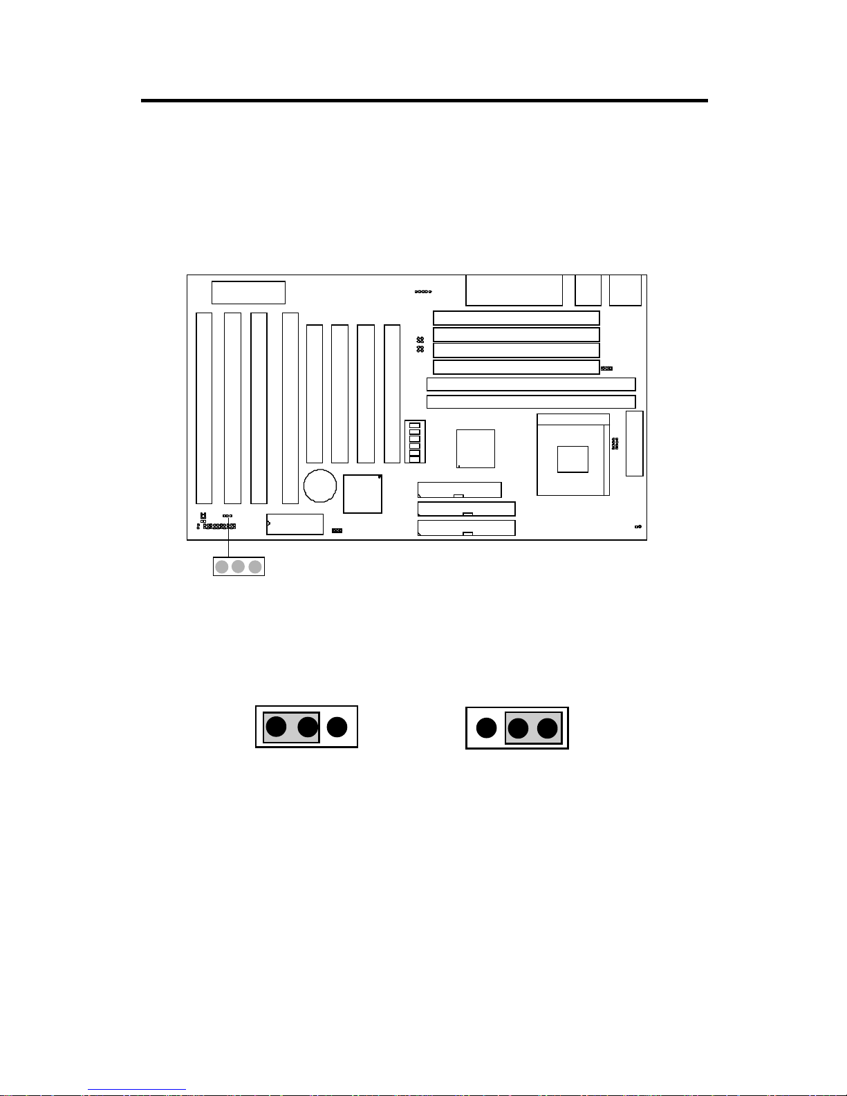
2.2 Flash ROM Programming Voltage: JP2
This jumper is for setting the V oltage of the Flash ROM BIOS.
13
13
+12V
+5V
(default)
Voltage Setting
1
JP4
3
SIMM1
SIMM2
SIMM3
SIMM4
DIMM1
DIMM2
Socket 7
FDD
IDE1
IDE2
ISA SLOT 4
ISA SLOT 2
ISA SLOT 3
ISA SLOT 1
PCI SLOT 4
PCI SLOT 3
PCI SLOT 2
PCI SLOT 1
BIOS
BATT
+
2032
JPF
JGS
JGL
JP2
INTEL
FW82371AB
INTEL
FW82439TX
JBAT
JRMS2
JFAN
ATX
POWER CONNECTOR
KBC
IR
JV1
LPT
COMA & COMB
USB
PS/2
JV3
JV4
JV5
SW
ON
DIP
121
3
4
1
5
6
JV6
JRMS1
+
JP2
2-9
2
2
Note: a. If you use Winbond , SST Flash ROM short 1-2 pin.
b. If you use Intel or MXIC Flash ROM short 1-2 pin, if you want to
flash the ROM data, short 2-3 pin , then put it back to 1-2 pin.
Page 15
CHAPTER 2 HARDWARE INSTALLATION
123
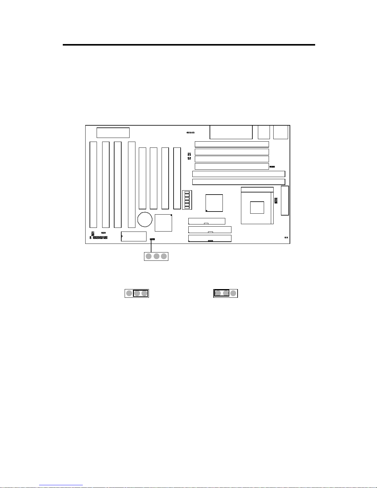
2.3 External Battery Connector: JBAT
A battery must be used to retain the system board configuration in CMOS
RAM. If you use the on-board battery you must short pins 1,2 of JBAT to
keep the CMOS data.
JBAT
12
SIMM1
SIMM2
SIMM3
SIMM4
DIMM1
DIMM2
Socket 7
FDD
IDE1
IDE2
ISA SLOT 4
ISA SLOT 2
ISA SLOT 3
ISA SLOT 1
PCI SLOT 4
PCI SLOT 3
PCI SLOT 2
PCI SLOT 1
BIOS
BATT
+
2032
JPF
JGS
JGL
JP2
INTEL
FW82371AB
INTEL
FW82439TX
JBAT
JRMS2
JFAN
ATX
POWER CONNECTOR
KBC
IR
JV1
LPT
COMA & COMB
USB
PS/2
JV3
JV4
JV5
SW
ON
DIP
121
3
4
1
5
6
JV6
JRMS1
+
2-10
3
123
Keep Data
Clear Data
Page 16
CHAPTER 2 HARDWARE INSTALLATION
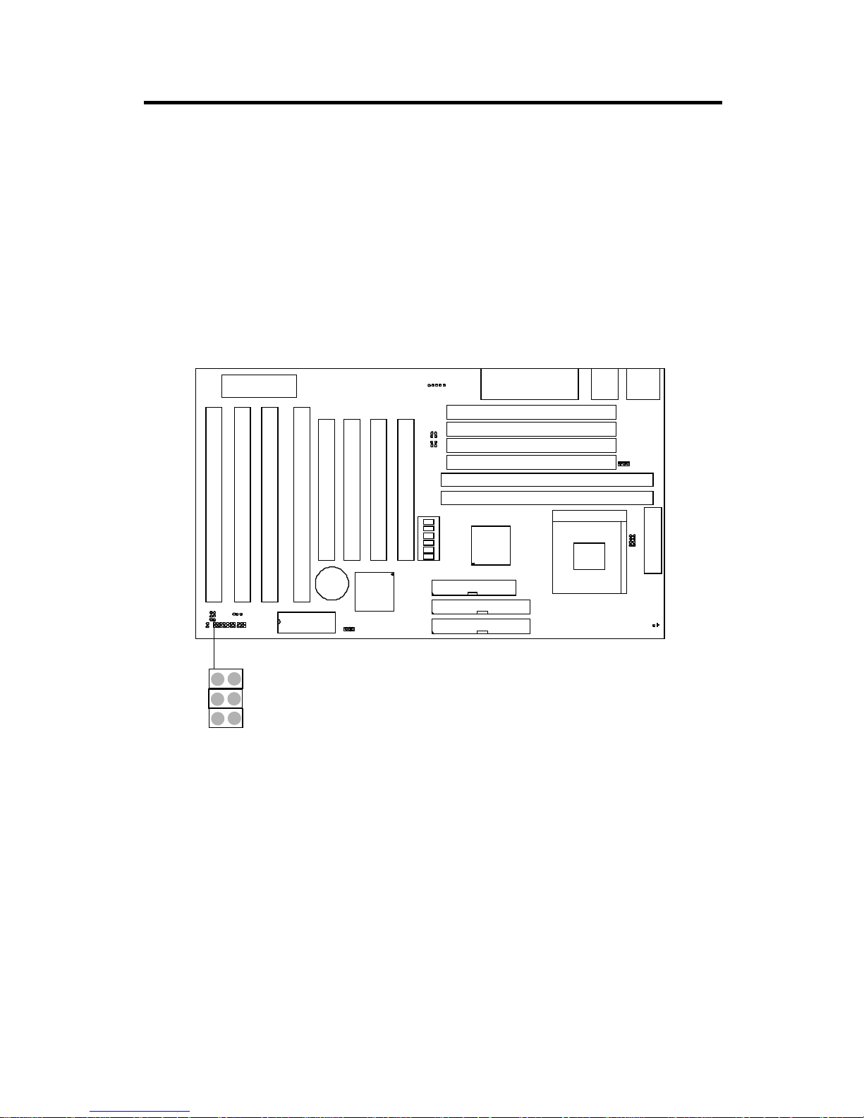
2.4 Power Saving Switch Connector: JGS/
Power Saving LED Connector: JGL
Attach a power saving switch to JGS. When the switch is pressed, the
system immediately goes into suspend mode. Press any key and the system
wakes up. JGL can be connected with LED to monitor the JGS.
JGS
SIMM1
SIMM2
SIMM3
SIMM4
DIMM1
DIMM2
Socket 7
FDD
IDE1
IDE2
ISA SLOT 4
ISA SLOT 2
ISA SLOT 3
ISA SLOT 1
PCI SLOT 4
PCI SLOT 3
PCI SLOT 2
PCI SLOT 1
BIOS
BATT
+
2032
JPF
JGS
JGL
JP2
INTEL
FW82371AB
INTEL
FW82439TX
JBAT
JRMS2
JFAN
ATX
POWER CONNECTOR
KBC
IR
JV1
LPT
COMA & COMB
USB
PS/2
JV3
JV4
JV5
SW
ON
DIP
121
3
4
1
5
6
JV6
JRMS1
+
JGL
2-11
Page 17
CHAPTER 2 HARDWARE INSTALLATION
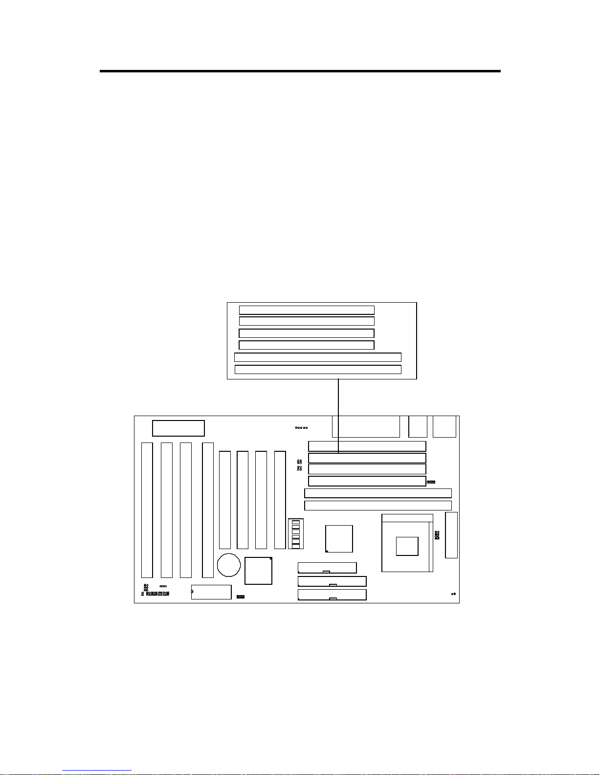
SIMM1(Bank 0)
SIMM2(Bank 0)
SIMM3(Bank 1)
SIMM4(Bank 1)
2-12
SIMM1
SIMM2
SIMM3
SIMM4
DIMM1
DIMM2
Socket 7
FDD
IDE1
IDE2
ISA SLOT 4
ISA SLOT 2
ISA SLOT 3
ISA SLOT 1
PCI SLOT 4
PCI SLOT 3
PCI SLOT 2
PCI SLOT 1
BIOS
BATT
+
2032
JPF
JGS
JGL
JP2
INTEL
FW82371AB
INTEL
FW82439TX
JBAT
JRMS2
JFAN
ATX
POWER CONNECTOR
KBC
IR
JV1
LPT
COMA & COMB
USB
PS/2
JV3
JV4
JV5
SW
ON
DIP
121
3
4
1
5
6
JV6
JRMS1
+
DIMM1(Bank 2)
DIMM2 (Bank 3)
2.5 Memory Installation
2.5-1 Memory Bank Configuration
The system board provides four 72-pin SIMMs (Single In-Line Memory Module) and two 168-pin DIMM(Double In-Line Memory) sockets, supports a
maximum of 256MB of memory . Y ou can use SIMM from 4MB, 8MB, 16MB,
32MB, 64MB or 128MB. And DIMM from 8MB, 16MB, 32MB, 64MB, 128MB,
or 256MB. A Bank consist of 2 SIMM socket or One DIMM socket. It also
consist of 2 RAS, each RAS supports memory up to 128MB.This board support 6 RAS.
Page 18
CHAPTER 2 HARDWARE INSTALLATION
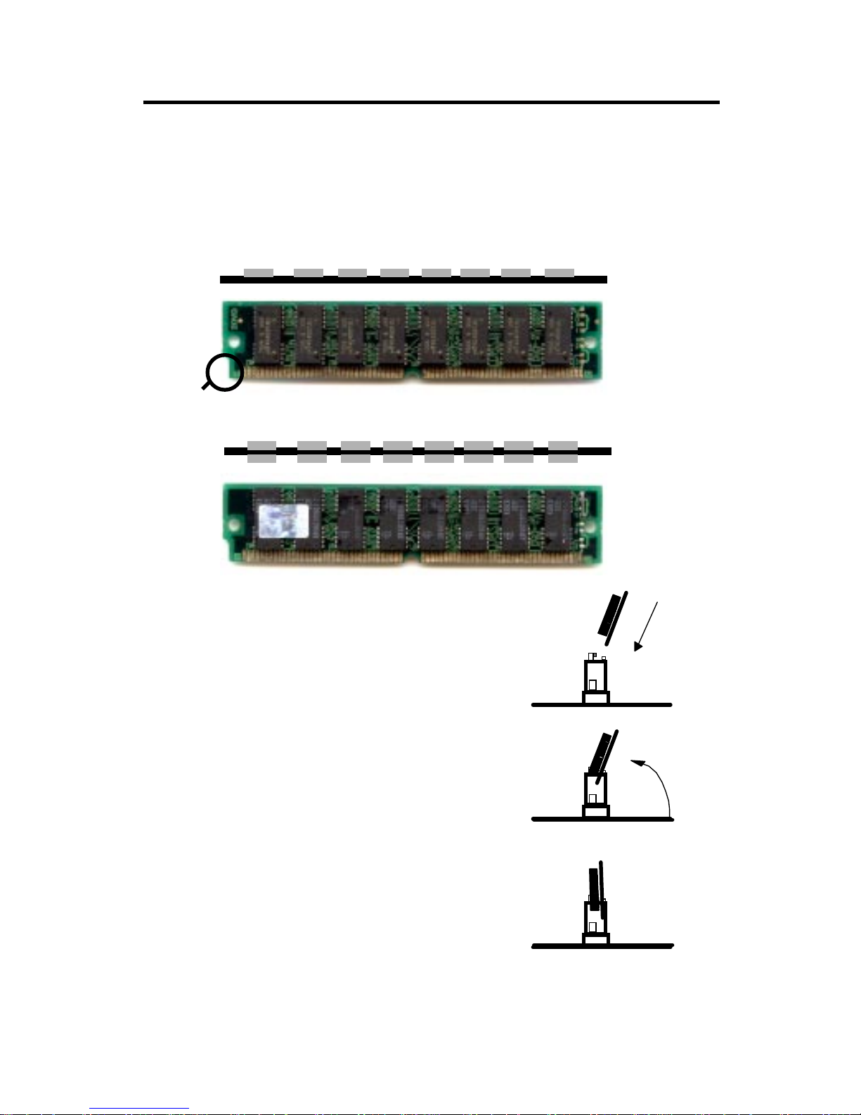
2.5-2 Memory Installation Procedures:
1. The SIMM slot has a “Plastic Safety
Tab” and the SIMM memory module
has a “Notched End”, so the SIMM
memory module can only fit in one
direction.
2. Insert the SIMM memory modules into
the socket at 45-degree angle, then
push into a vertical position so that it
will snap into place.
3. The Mounting Holes and Metal Clips
should fit over the edge and hold the
SIMM memory modules in place.
A. How to install a SIMM Module
Single Sided SIMM
Double Sided SIMM
Notched
End
2-13
Page 19
CHAPTER 2 HARDWARE INSTALLATION
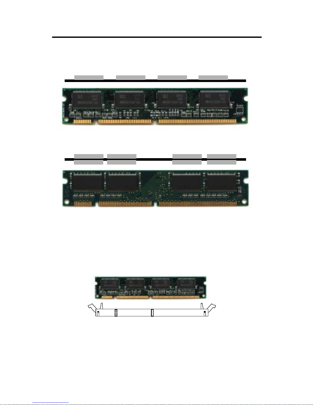
B. How to install a DIMM Module
1. The DIMM slot has a two key mark “VOLT and DRAM” , so the
DIMM memory module can only fit in one direction.
2. Insert the DIMM memory module vertically into the DIMM slot
then push it in.
3. Close the plastic clip at the side of the DIMM slot.
Single Sided DIMM
Double Sided DIMM
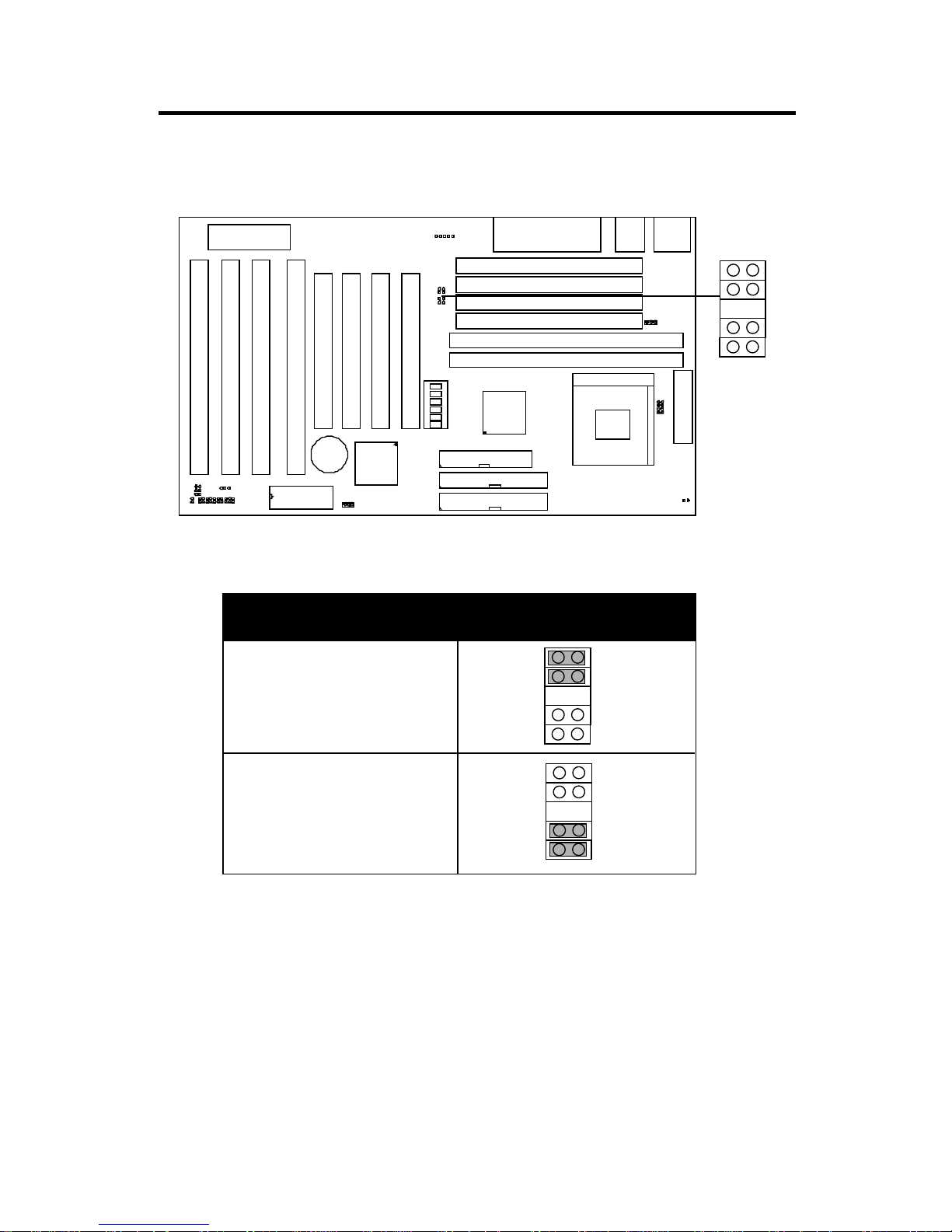
Note: If you have installed SIMM and DIMM at the same time. Y ou must
use a 3.3 volt DIMM with 5 volt I/O signal tolerance or a full 5 volt
DIMM module (EDO, FP or SDRAM). Look for JV1 to select the
DIMM voltage.
2-14
Page 20
CHAPTER 2 HARDWARE INSTALLATION
2-15
B.1 DIMM Power V oltage Selector : JV1
DIMM V oltage JV1
5V
3.3V
SIMM Power Level : 5 Volts DIMM Power Level : 3.3V or 5V
SIMM1
SIMM2
SIMM3
SIMM4
DIMM1
DIMM2
Socket 7
FDD
IDE1
IDE2
ISA SLOT 4
ISA SLOT 2
ISA SLOT 3
ISA SLOT 1
PCI SLOT 4
PCI SLOT 3
PCI SLOT 2
PCI SLOT 1
BIOS
BATT
+
2032
JPF
JGS
JGL
JP2
INTEL
FW82371AB
INTEL
FW82439TX
JBAT
JRMS2
JFAN
ATX
POWER CONNECTOR
KBC
IR
JV1
LPT
COMA & COMB
USB
PS/2
JV3
JV4
JV5
SW
ON
DIP
121
3
4
1
5
6
JV6
JRMS1
+
JV1
+5V
+3V
Page 21

CHAPTER 2 HARDWARE INSTALLATION
1. Make sure that the SIMM banks are using the same type and equal size
density memory.
2 . To operate properly at least two 72-pin SIMM module must be installed in
the same bank or one 168-pin DIMM module must be installed.
3. Look at the table below:
4 . Before using SIMM and DIMM modules, look at the chart next page.
5 . Each RAS can not exceed 16 pcs of DRAM.
6. It is not recommended to mix 3V SDRAM with 5V EDO/FP , for it may
cause unreliability.
6 . If SDRAM and EDO/FPM are mixed in a system, then the configuration is
limited to a miximum of four RAS(two RAS of x4 EDO/FPM and two RAS
of x8 or x16 SDRAM). If only x8 or x16 EDO/FPM and SDRAM devices
are used(i.e. not x4’ s), then five RAS can be supported.
7 . If you use a 64M DRAM of SDRAM, then Bank0 can not be use.
2.5-3 Memory Population Rule
BANK0 BANK1 BANK2 BANK3
S S/D/N S/D/N S/N
D S/D/N S/D/N N
N S/D/N S/D/N D
S = Single Density D = Double Density N = None
2-16
Page 22

CHAPTER 2 HARDWARE INSTALLATION
4M 1Mx4 SYMM 10 10 4MBx8 8MBx16
16M 1Mx16 SYMM 10 10 4MBx2 8MBx4
1Mx16 ASYM 12 8 4MBx2 8MBx4
2Mx8 ASYM 11 10 8MBx4 16MBx8
4Mx4 SYMM 11 11 16MBx8 32MBx16
4Mx4 ASYM 12 10 16MBx8 32MBx16
64M 2Mx32 ASYM 12 9 8MBx1 16MBx2
4Mx16 SYMM 11 11 16MBx2 32MBx4
4Mx16 ASYM 12 10 16MBx2 32MBx4
8Mx8 ASYM 12 11 32MBx4 64MBx8
16Mx4 SYMM 1 2 12 64MBx8128MBx16
16M 1Mx16 ASYM 12 8 8MBx4 16MBx8
2Mx8 ASYM 12 9 16MBx8 32MBx16
4Mx4 ASYM 12 10 32MB 64MB
64M 2Mx32 ASYM 12 10 32MBx2 64MBx4
2Mx32 ASYM 13 8 16MBx2 32MBx4
4Mx16 ASYM 14 8 32MB 64MB
8Mx8 ASYM 14 9 64MB 128MB
16Mx4 ASYM 14 10 128MB 256MB
DRAM
Tech.
DRAM
Density &
Width
DRAM
Addressing
Address Size
MB/SIMM
Row
Column
Single
Side(S)
Double
Side(D)
DRAM
Tech.
DRAM
Density &
Width
DRAM
Addressing
Address Size
MB/DIMM
Row
Column
Single
Side(S)
Double
Side(D)
Table 2.5-1 Minimum (upgradeable) and Maximum
Memory Size for each configuration for SIMM
Table 2.5-2 Minimum (upgradeable) and Maximum
Memory Size for each configuration for DIMM
2-17
no.
pcs.
no.
pcs.
no.
pcs.
no.
pcs.
Page 23
CHAPTER 2 HARDWARE INSTALLATION
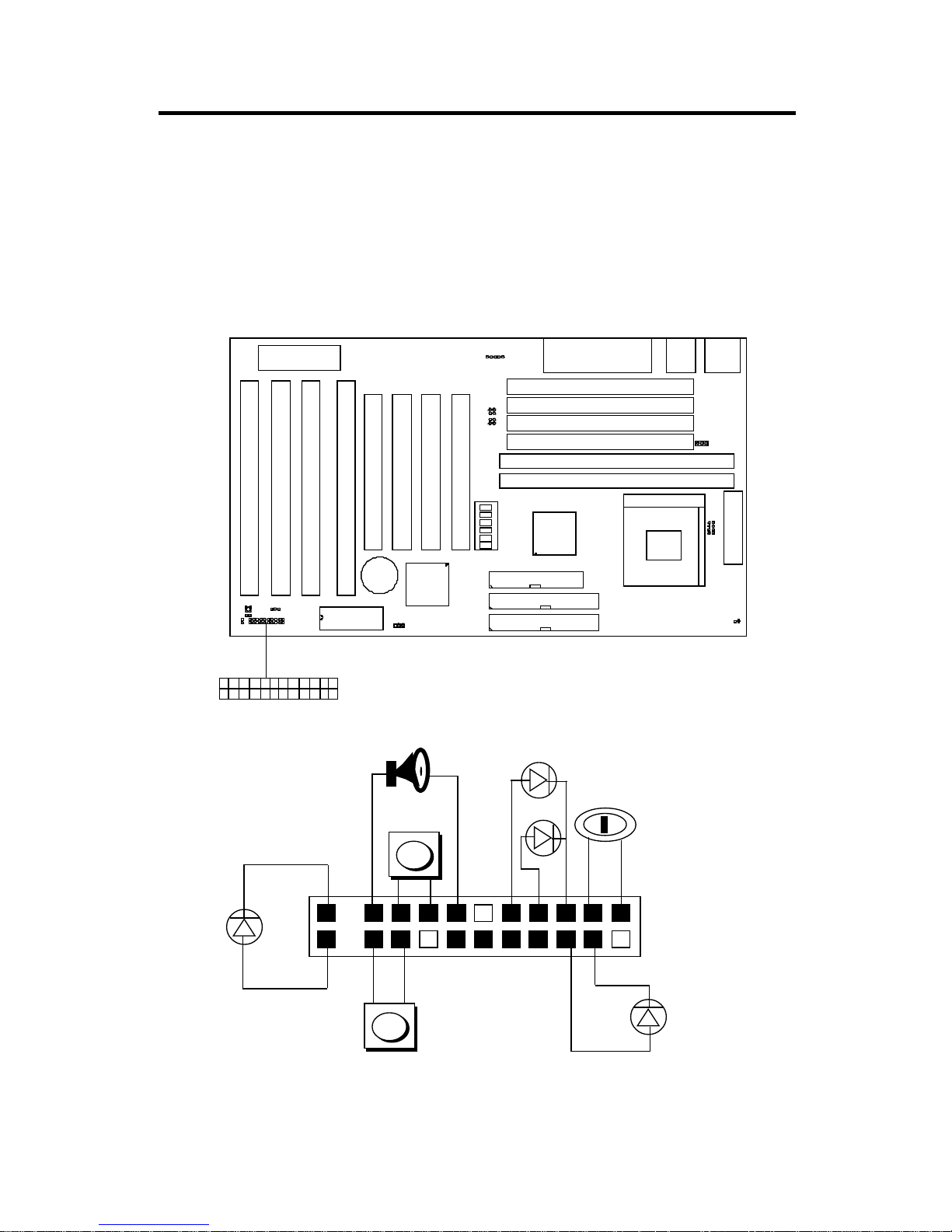
2.6 Case Connector: JFP
The Turbo LED, Hardware Reset, Key Lock, Power LED, Power Saving LED,
Sleep Switch, Speaker and HDD LED all connected to the JFP connector
block.
1
JFP
10
21
1
x
x
1122
21
Speaker
Power LED
Keylock
Turbo LED
Reset Switch
HDD LED
10
20
+
+
+
Sleep
Switch
+
Power
Saving
LED
Figure 2.1
2-18
SIMM1
SIMM2
SIMM3
SIMM4
DIMM1
DIMM2
Socket 7
FDD
IDE1
IDE2
ISA SLOT 4
ISA SLOT 2
ISA SLOT 3
ISA SLOT 1
PCI SLOT 4
PCI SLOT 3
PCI SLOT 2
PCI SLOT 1
BIOS
BATT
+
2032
JPF
JGS
JGL
JP2
INTEL
FW82371AB
INTEL
FW82439TX
JBAT
JRMS2
JFAN
ATX
POWER CONNECTOR
KBC
IR
JV1
LPT
COMA & COMB
USB
PS/2
JV3
JV4
JV5
SW
ON
DIP
121
3
4
1
5
6
JV6
JRMS1
+
Page 24

CHAPTER 2 HARDWARE INSTALLATION
2-19
2.6-1 Turbo LED
The T urbo LED are always ON. You can connect the Turbo LED from the
system case to this pin. (See Figure 2.1)
2.6-2 Hardware Reset
Reset switch are use to reboot the system rather than turning the power ON/
OFF , but avoid rebooting will the HDD LED is lit. You can connect the Reset
switch form the system case to this pin. (See Figure 2.1)
2.6-3 Keylock
Keylock allows you to disabled the keyboard for security purposes. You
can connect the keylock to this pin. (See Figure 2.1)
2.6-4 Power LED
The Power LED is always lit while the system power is on. You can connect
the Power LED form the system case to this pin. (See Figure 2.1)
2.6-5 Suspend Switch
The Suspend Switch can be set in the BIOS Power Management Setup.
When used as a Suspend Switch, this allows the user to suspend the
system when not in use. (See Figure 2.1)
2.6-6 Speaker
Speaker from the system case are connected to this pin. (See Figure 2.1)
2.6-7 HDD LED
HDD LED shows the activity of a hard disk drive. Avoid tuning the power
off while the HDD led is lit. You can connect the HDD LED from the system
case to this pin. (See Figure 2.1).
Page 25
CHAPTER 2 HARDWARE INSTALLATION
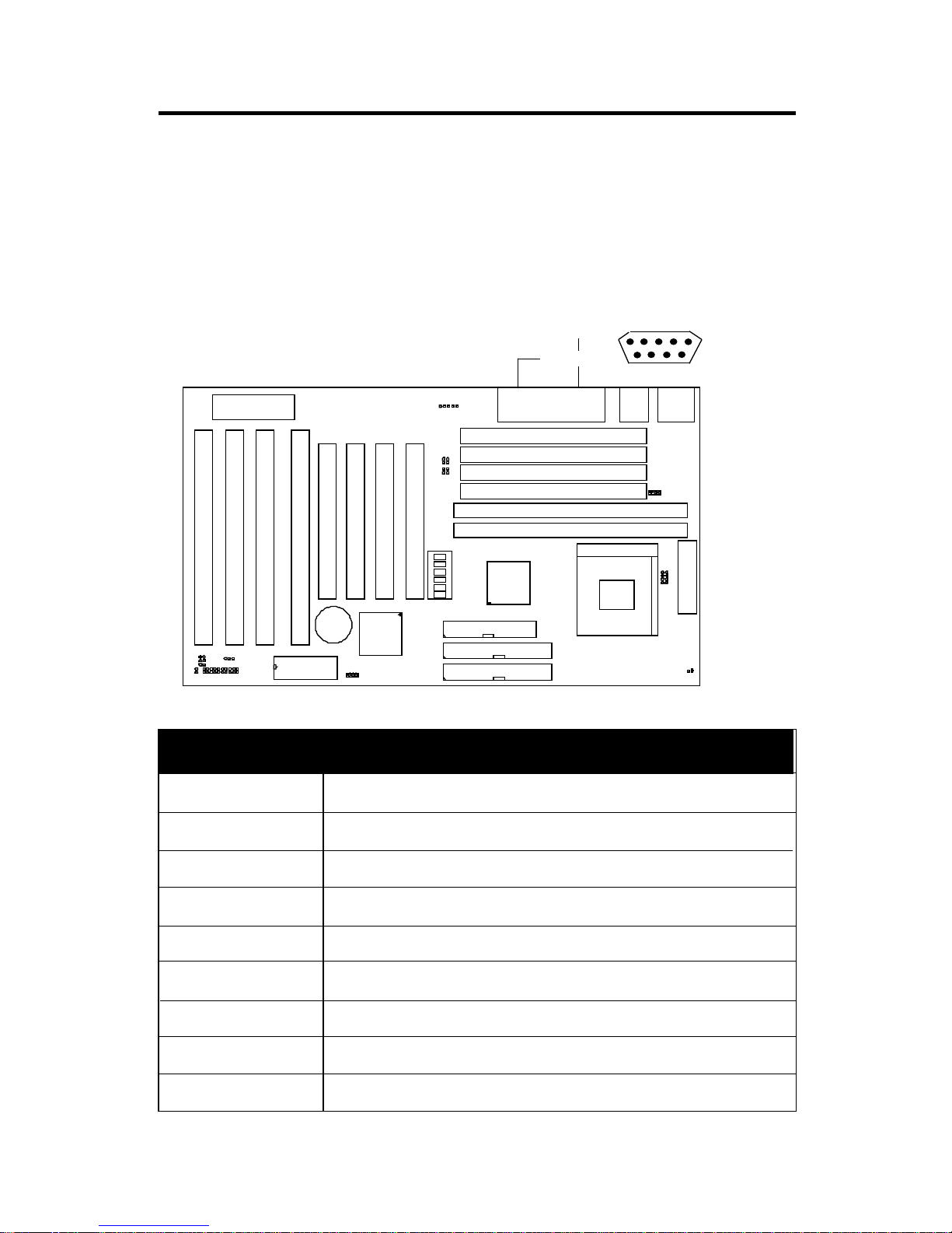
2.7 Serial Port Connectors: COMA & COMB
The system board has two serial ports COMA and COMB. These two ports
are 16550A high speed communication ports that send/receive 16 bytes
FIFOs. You can attach a mouse or a modem cable directly into these connectors.
2-20
SIMM1
SIMM2
SIMM3
SIMM4
DIMM1
DIMM2
Socket 7
FDD
IDE1
IDE2
ISA SLOT 4
ISA SLOT 2
ISA SLOT 3
ISA SLOT 1
PCI SLOT 4
PCI SLOT 3
PCI SLOT 2
PCI SLOT 1
BIOS
BATT
+
2032
JPF
JGS
JGL
JP2
INTEL
FW82371AB
INTEL
FW82439TX
JBAT
JRMS2
JFAN
ATX
POWER CONNECTOR
KBC
IR
JV1
LPT
COMA & COMB
USB
PS/2
JV3
JV4
JV5
SW
ON
DIP
121
3
4
1
5
6
JV6
JRMS1
+
1 2 3 4 5
6 7 8 9
COMB
COMA
PIN DEFINITION
Pin # Definition
1 DCD(Data Carry Detect)
2 SIN(Serial In or Receive Data)
3 SOUT(Serial Out or Transmit Data)
4 DTR(Data Terminal Ready)
5 GND
6 DSR(Data Set Ready)
7 RTS(Request To Send)
8 CTS(Clear To Send)
9 RI(Ring Indicate)
Page 26
CHAPTER 2 HARDWARE INSTALLATION
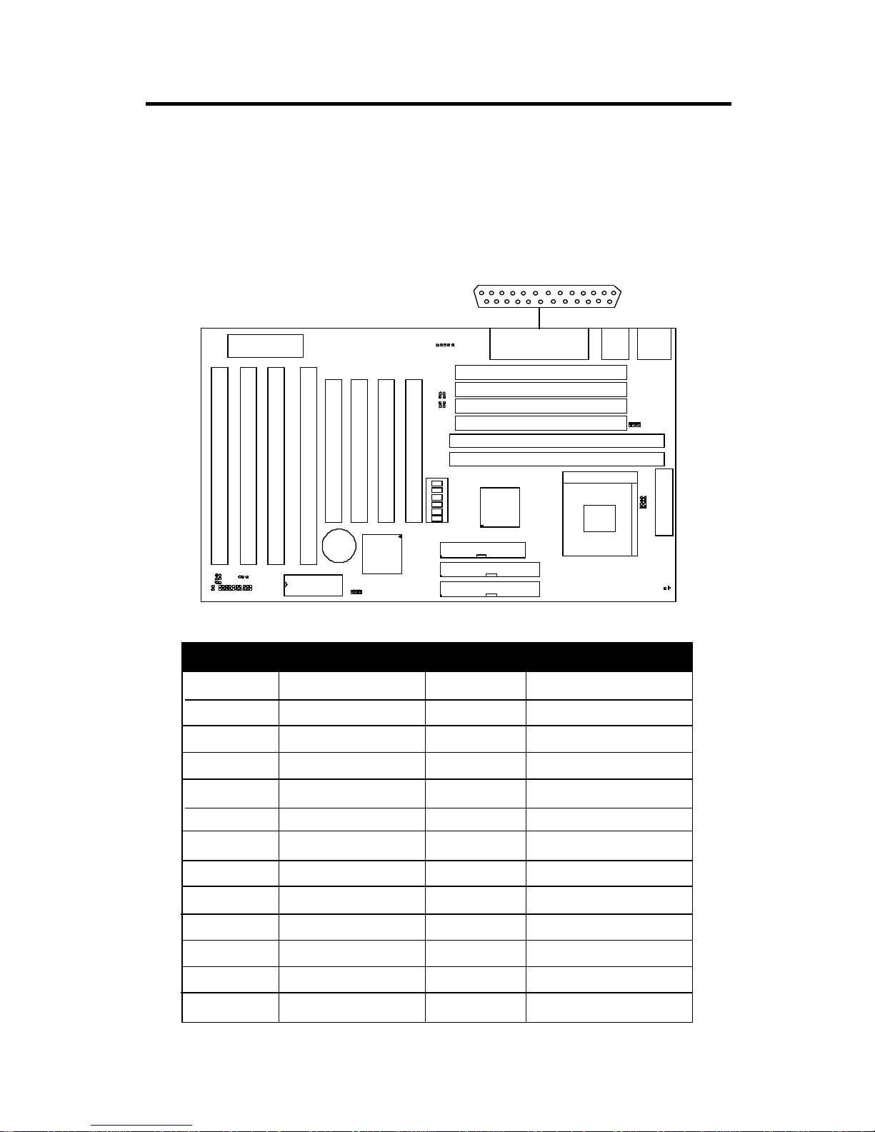
2.8 Parallel Port Connectors: LPT
The system board provides a connector for LPT. A parallel port is a standard printer port that also supports Enhanced Parallel Port(EPP) and Extended
capabilities Parallel Port(ECP).
2-21
SIMM1
SIMM2
SIMM3
SIMM4
DIMM1
DIMM2
Socket 7
FDD
IDE1
IDE2
ISA SLOT 4
ISA SLOT 2
ISA SLOT 3
ISA SLOT 1
PCI SLOT 4
PCI SLOT 3
PCI SLOT 2
PCI SLOT 1
BIOS
BATT
+
2032
JPF
JGS
JGL
JP2
INTEL
FW82371AB
INTEL
FW82439TX
JBAT
JRMS2
JFAN
ATX
POWER CONNECTOR
KBC
IR
JV1
LPT
COMA & COMB
USB
PS/2
JV3
JV4
JV5
SW
ON
DIP
121
3
4
1
5
6
JV6
JRMS1
+
13 12 11 10 9 8 7 6 5 4 3 2 1
25 24 23 22 21 20 19 18 17 16 15 14
LPT
PIN # DEFINITION PIN # DEFINITION
1 STROBE 14 AUTO FEED#
2 DATA0 15 ERR#
3 DA TA1 16 INIT#
4 DATA2 17 SLIN#
5 DATA3 18 GND
6 DATA4 19 GND
7 DATA5 20 GND
8 DATA6 21 GND
9 DATA7 22 GND
10 ACK# 23 GND
11 BUSY 24 G N D
12 P E 25 GND
13 SELECT
PIN DEFINITION
Page 27
CHAPTER 2 HARDWARE INSTALLATION
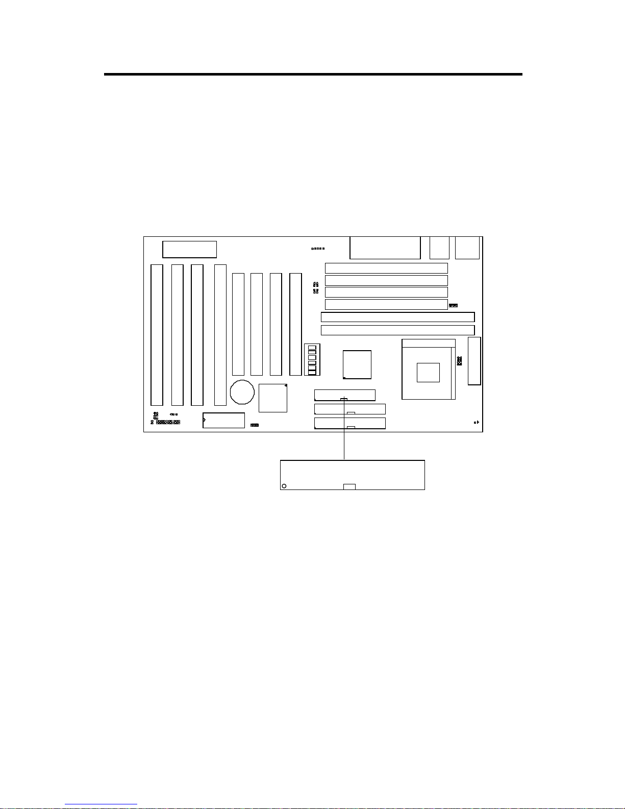
2.9 Floppy Disk Connector: FDD
The system board also provides a standard floppy disk connector FDD that
supports 360K, 720K, 1.2M, 1.44M and 2.88M floppy disk types. You can
attach a floppy disk cable directly to this connector.
FDD
1
2-22
SIMM1
SIMM2
SIMM3
SIMM4
DIMM1
DIMM2
Socket 7
FDD
IDE1
IDE2
ISA SLOT 4
ISA SLOT 2
ISA SLOT 3
ISA SLOT 1
PCI SLOT 4
PCI SLOT 3
PCI SLOT 2
PCI SLOT 1
BIOS
BATT
+
2032
JPF
JGS
JGL
JP2
INTEL
FW82371AB
INTEL
FW82439TX
JBAT
JRMS2
JFAN
ATX
POWER CONNECTOR
KBC
IR
JV1
LPT
COMA & COMB
USB
PS/2
JV3
JV4
JV5
SW
ON
DIP
121
3
4
1
5
6
JV6
JRMS1
+
Page 28
CHAPTER 2 HARDWARE INSTALLATION
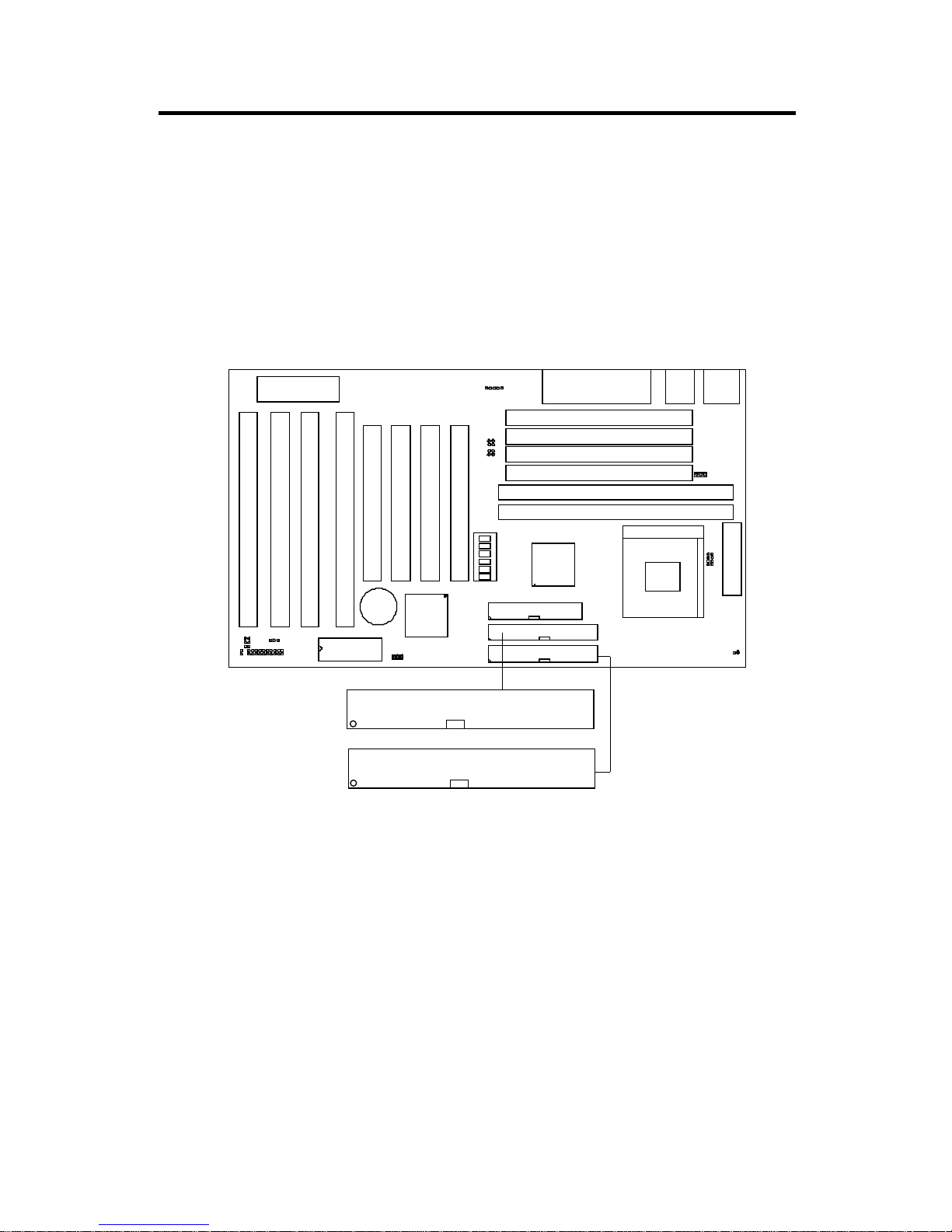
2.10 Hard Disk Connector: IDE1 & IDE2
The system board has a 32-bit Enhanced PCI IDE Controller that provide PIO
mode 4 Ultra DMA33 speed. It has two HDD connectors IDE1 (primary) and
IDE2 (secondary). You can connect up to four hard disk drives, CD-ROM,
120MB Floopy (reserved for future BIOS) and other devices to IDE1 and
IDE2.
Primary IDE Connector
Secondary IDE Connector
IDE1(primary IDE connector)
The first hard disk should always be connected to IDE1. IDE1 can
connect a Master and a Slave drive.
IDE2(secondary IDE connector)
IDE2 can also connect a Master and a Slave drive.
1
1
SIMM1
SIMM2
SIMM3
SIMM4
DIMM1
DIMM2
Socket 7
FDD
IDE1
IDE2
ISA SLOT 4
ISA SLOT 2
ISA SLOT 3
ISA SLOT 1
PCI SLOT 4
PCI SLOT 3
PCI SLOT 2
PCI SLOT 1
BIOS
BATT
+
2032
JPF
JGS
JGL
JP2
INTEL
FW82371AB
INTEL
FW82439TX
JBAT
JRMS2
JFAN
ATX
POWER CONNECTOR
KBC
IR
JV1
LPT
COMA & COMB
USB
PS/2
JV3
JV4
JV5
SW
ON
DIP
121
3
4
1
5
6
JV6
JRMS1
+
2-23
Page 29
CHAPTER 2 HARDWARE INSTALLATION
2-24
2.12 Power Supply
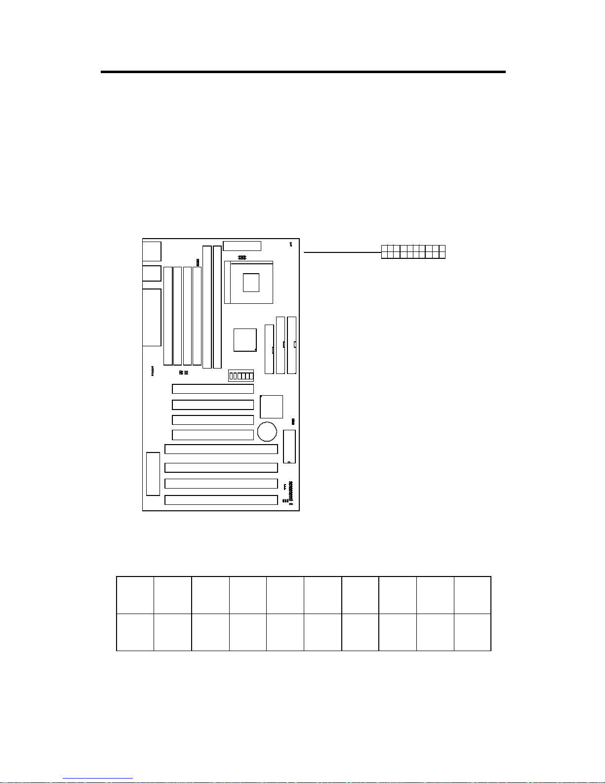
2.12-1 ATX 20-pin Power Connector: JWR12
This connector support the power button on board soft power off and
modem ring wakeup. you neeed to use the push button JRMS1 and
JRMS2.
10..................................1
20................................11
5V 5V -5V
5V5V
3.3V-12V
12V
5V_SB
3.3V
3.3V
GNDGND
GND
GND
GNDGND
GND
PW_Ok
PS_ON
1
23
456
7
8
9
10
11
1213
14
15
16
1718
19
20
A TX Power Connector Pin Description
ATX
Power Connector
SIMM1
SIMM2
SIMM3
SIMM4
DIMM1
DIMM2
Socke t 7
FDD
IDE1
IDE2
ISA SLOT 4
ISA SLOT 2
ISA SLOT 3
ISA SLOT 1
PCI SLOT 4
PCI SLOT 3
PCI SLOT 2
PCI SLOT 1
BIOS
BATT
+
2032
JPF
JGS
JGL
JP2
INTEL
FW82371AB
INTEL
FW82439TX
JBAT
JRMS2
JFAN
ATX
POWER CONNECTOR
KBC
IR
JV1
LPT
COMA & COMB
USB
PS/2
JV3
JV4
JV5
SW
ON
DIP
121
3
4
1
5
6
JV6
JRMS1
+
Page 30
CHAPTER 2 HARDWARE INSTALLATION
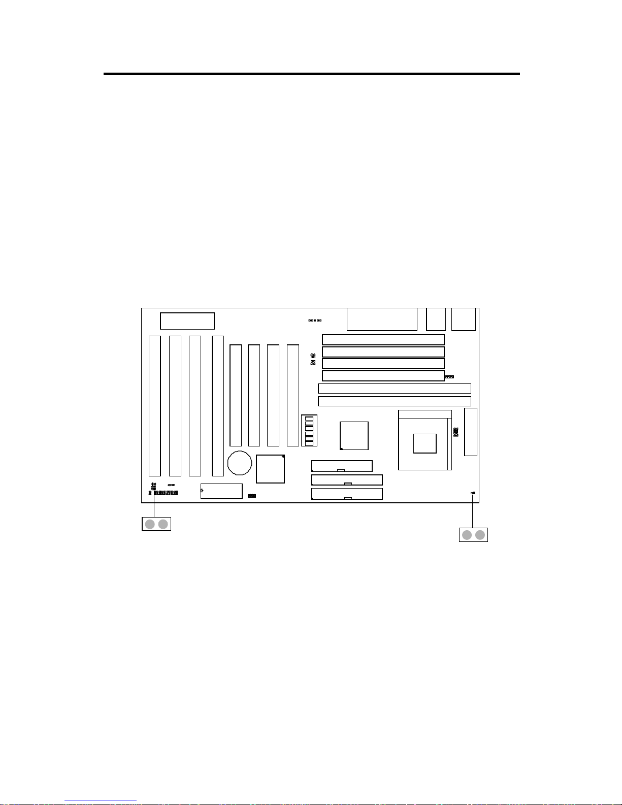
2.12-2 Power On/Off Switch: JRMS1/JRMS2
Connect to a 2-pin push button switch. Every time the switch is shorted by
pushing it once, the power supply will change its status from OFF to ON.
During ON stage push once and the system goes to sleep mode, push it
more than 4 seconds will change its status fr om ON to OFF. If you want to
change the setup, you could go the BIOS setup and look for Power Management Setup.
JRMS2
SIMM1
SIMM2
SIMM3
SIMM4
DIMM1
DIMM2
Socket 7
FDD
IDE1
IDE2
ISA SLOT 4
ISA SLOT 2
ISA SLOT 3
ISA SLOT 1
PCI SLOT 4
PCI SLOT 3
PCI SLOT 2
PCI SLOT 1
BIOS
BATT
+
2032
JPF
JGS
JGL
JP2
INTEL
FW82371AB
INTEL
FW82439TX
JBAT
JRMS2
JFAN
ATX
POWER CONNECTOR
KBC
IR
JV1
LPT
COMA & COMB
USB
PS/2
JV3
JV4
JV5
SW
ON
DIP
121
3
4
1
5
6
JV6
JRMS1
+
JRMS1
Note: The two switch provided by the board is just for your convenience,
The two switch has the same feature.
2-25
Page 31
CHAPTER 2 HARDWARE INSTALLATION
2-26
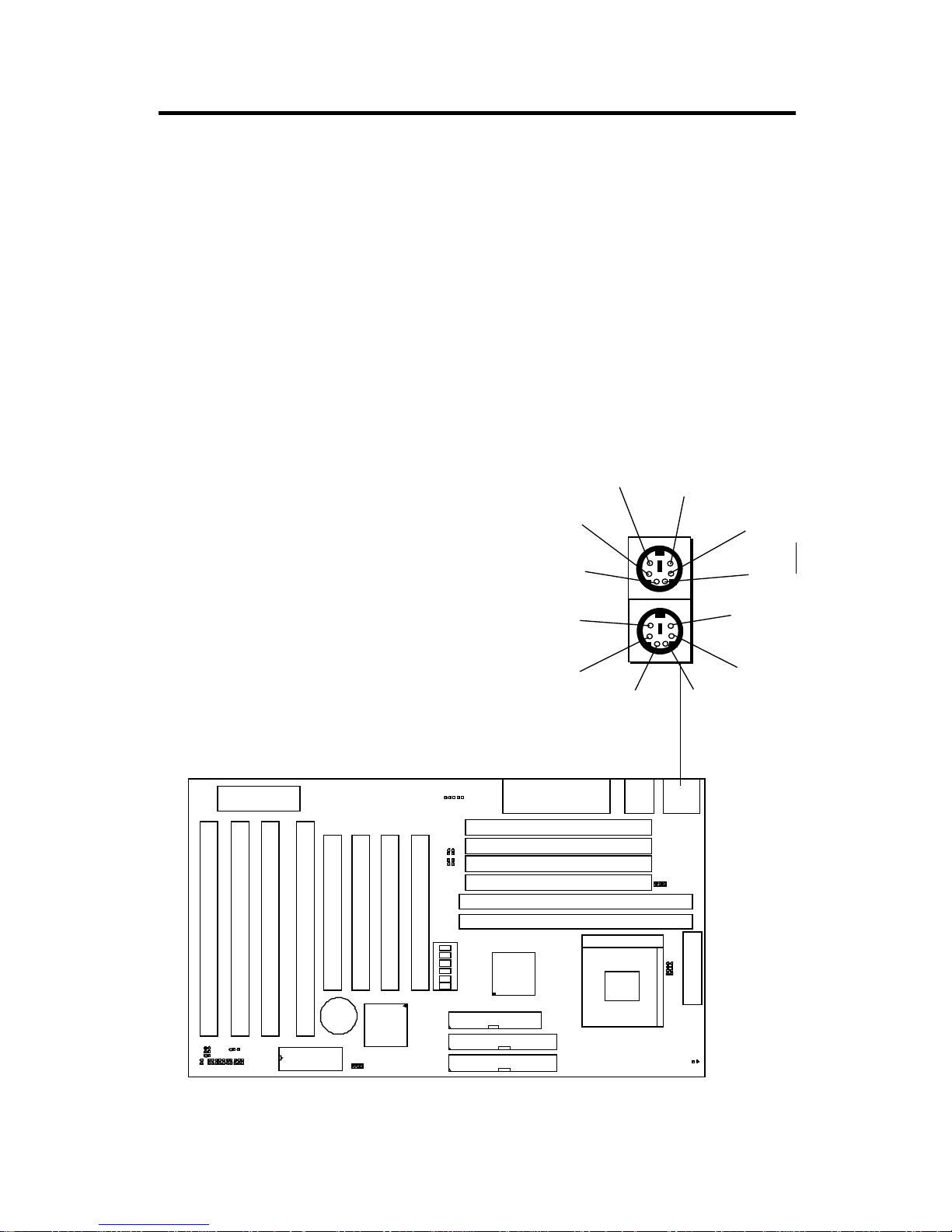
2.13 Keyboard Connector: PSKBC
Mouse Connector: PSMSC
The system board provides a standard PS/2 style keyboard mini DIN
connector for attaching a keyboard. You can plug a keyboard cable directly
to this connector.
It also provides a standard PS/2 style mouse mini DIN connector for attaching a PS/2 style mouse. You can plug a PS/2 style mouse directly into this
connector . The connector location and pin definition as shown below:
Pin6
NC
Pin4
VCC
Pin1
Mouse
DATA
Pin6
NC
Pin2
NC
Pin4
VCC
Pin3
GND
Pin5
Mouse
Clock
Pin1
KBD DATA
Pin2
NC
Pin3
GND
Pin5
KBD Clock
SIMM1
SIMM2
SIMM3
SIMM4
DIMM1
DIMM2
Socket 7
FDD
IDE1
IDE2
ISA SLOT 4
ISA SLOT 2
ISA SLOT 3
ISA SLOT 1
PCI SLOT 4
PCI SLOT 3
PCI SLOT 2
PCI SLOT 1
BIOS
BATT
+
2032
JPF
JGS
JGL
JP2
INTEL
FW82371AB
INTEL
FW82439TX
JBAT
JRMS2
JFAN
ATX
POWER CONNECTOR
KBC
IR
JV1
LPT
COMA & COMB
USB
PS/2
JV3
JV4
JV5
SW
ON
DIP
121
3
4
1
5
6
JV6
JRMS1
+
PSKBC
PSMSC
Page 32
CHAPTER 2 HARDWARE INSTALLATION
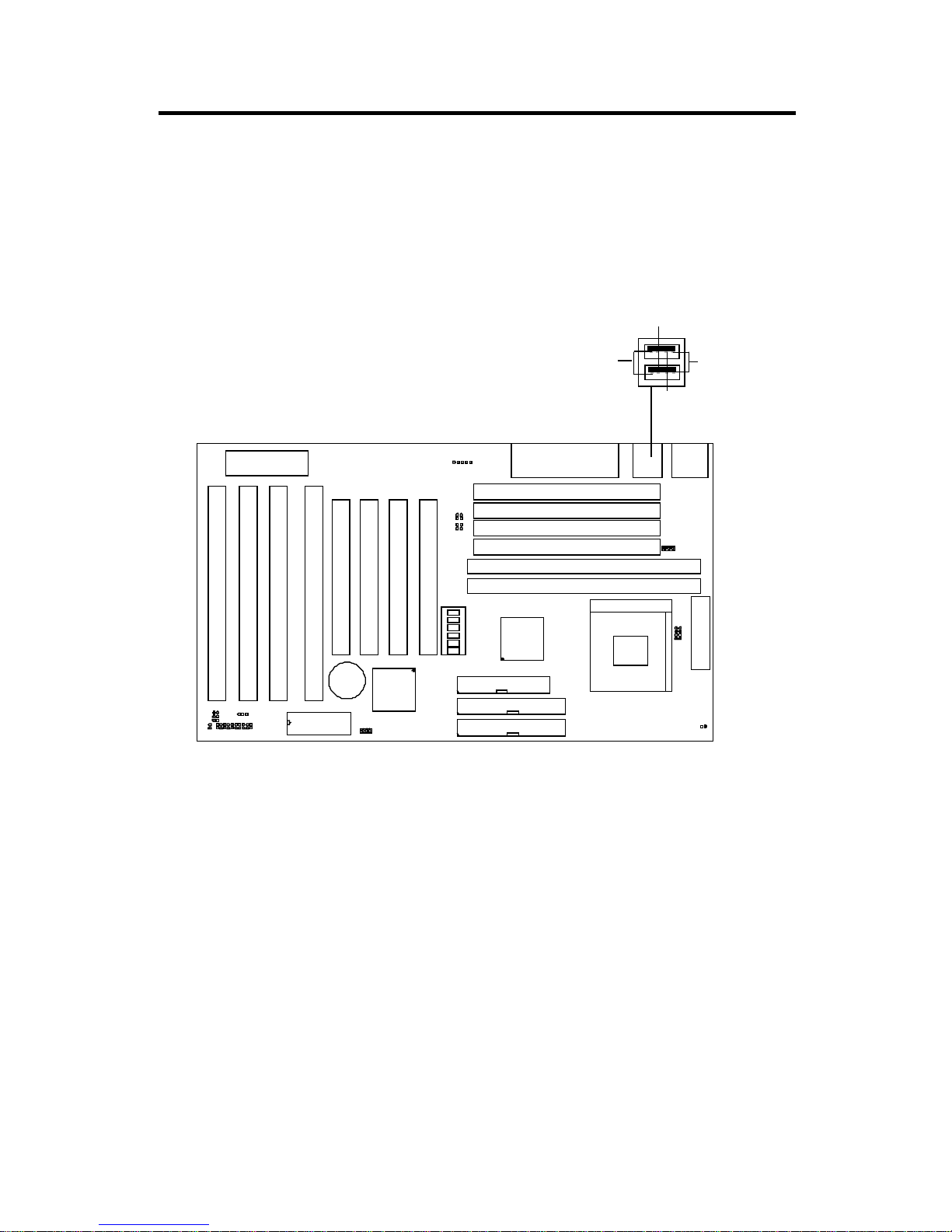
2.14 USB Connector: USB
The system board provide a USB(Universal Serial Bus) connector for
attaching a keyboard, mose or etc. You can plug it directly to this connectro.
2-27
SIMM1
SIMM2
SIMM3
SIMM4
DIMM1
DIMM2
Socket 7
FDD
IDE1
IDE2
ISA SLOT 4
ISA SLOT 2
ISA SLOT 3
ISA SLOT 1
PCI SLOT 4
PCI SLOT 3
PCI SLOT 2
PCI SLOT 1
BIOS
BATT
+
2032
JPF
JGS
JGL
JP2
INTEL
FW82371AB
INTEL
FW82439TX
JBAT
JRMS2
JFAN
ATX
POWER CONNECTOR
KBC
IR
JV1
LPT
COMA & COMB
USB
PS/2
JV3
JV4
JV5
SW
ON
DIP
121
3
4
1
5
6
JV6
JRMS1
+
VCC
GND
DO-
DOT
USB
Connector
Page 33
CHAPTER 2 HARDWARE INSTALLATION
2-28
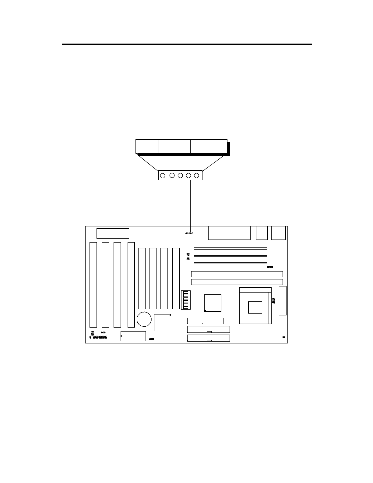
2.15 IrDA Infrared Module Connector: IR
The system board provides a 5-pin infrared connector(IR) for IR module.
This connector is for optional wireless transmitting and receiving infrared
module. You must configure the setting through BIOS setup.
IR
VCC NC RXGNDTX
SIMM1
SIMM2
SIMM3
SIMM4
DIMM1
DIMM2
Socket 7
FDD
IDE1
IDE2
ISA SLOT 4
ISA SLOT 2
ISA SLOT 3
ISA SLOT 1
PCI SLOT 4
PCI SLOT 3
PCI SLOT 2
PCI SLOT 1
BIOS
BATT
+
2032
JPF
JGS
JGL
JP2
INTEL
FW82371AB
INTEL
FW82439TX
JBAT
JRMS2
JFAN
ATX
POWER CONNECTOR
KBC
IR
JV1
LPT
COMA & COMB
USB
PS/2
JV3
JV4
JV5
SW
ON
DIP
121
3
4
1
5
6
JV6
JRMS1
+
Page 34

CHAPTER 3 AWARD BIOS SETUP
3-1
Chapter 3
AWARD BIOS SETUP
Award’s BIOS ROM has a built-in Setup program that allows users to modify
the basic system configuration. This type of information is stored in battery
-backed RAM (CMOS RAM), so that it retains the Setup information when
the power is turned off.
Page 35

CHAPTER 3 AWARD BIOS SETUP
3-2
3.1 Entering Setup
Power on the computer and press <Del> immediately will allow you to
enter Setup. The other way to enter Setup is to power on the computer ,
when the below message appears briefly at the bottom of the screen during
the POST (Power On Self Test), press <Del> key or simultaneously press
<Ctrl>, <Alt>, and <Esc> keys.
TO ENTER SETUP BEFORE BOOT PRESS <CTRL-AL T-ESC>
OR <DEL> KEY
If the message disappears before you respond and you still wish to
enter Setup, restart the system to try again by turning it OFF then ON or
pressing the “RESET” button on the system case. You may also restart by
simultaneously pressing <Ctrl>, <Alt>, and <Delete> keys. If you do not
press the keys at the correct time and the system does not boot, an error
message will be displayed and you will again be asked to,
PRESS <F1> TO CONTINUE, <CTRL-AL T-ESC>
OR <DEL> TO ENTER SETUP
3.2 Getting Help
Main Menu
The on-line description of the highlighted setup function is displayed
at the bottom of the screen.
Status Page Setup Menu/Option Page Setup Menu
Press F1 to pop up a small help window that describes the appropriate keys to use and the possible selections for the highlighted item. To exit
the Help W indow press <F1> or <Esc>.
Page 36

CHAPTER 3 AWARD BIOS SETUP
3-3
3.3 The Main Menu
Once you enter A ward BIOS CMOS Setup Utility , the Main Menu (Figure 1)
will appear on the screen. The Main Menu allows you to select from ten
setup functions and two exit choices. Use arrow keys to select among the
items and press <Enter> to accept or enter the sub-menu.
Figure 1 Main Menu
ROM PCI/ISA BIOS (2A59IM4A)
CMOS SETUP UTILITY
AWARD SOFTWARE, INC.
STANDARD CMOS SETUP
BIOS FEATURES SETUP
CHIPSET FEATURES SETUP
POWER MANAGEMENT SETUP
PNP/PCI CONFIGURATION
LOAD SETUP DEFAULTS
INTEGRATED PERIPHERALS
SUPERVISOR PASSWORD
USER PASSWORD
IDE HDD AUTO DETECTION
SAVE & EXIT SETUP
EXIT WITHOUT SAVING
Esc : Quit
F10 : Save & Exit Setup
Time, Date, Hard Disk Type...
↑ ↓ → ← : Select Item
(Shift)F2 : Change Color
Page 37

CHAPTER 3 AWARD BIOS SETUP
3-4
Standard CMOS Setup
This setup page includes all the items in a standard compatible BIOS.
BIOS Features Setup
This setup page includes all the items of A ward special enhanced
features.
Chipset Features Setup
This setup page includes all the items of chipset special features.
Power Management Setup
This category determines the power consumption for system after
setting the specified items. Default value is Disable.
PCI Configuration Setup
This category specifies the value (in units of PCI bus clocks) of the
latency timer for this PCI bus master and the IRQ level for PCI device.
Supervisor Password/User Password
Change set or disable password. This function allows the user
access to the system and setup or just setup.
Load Setup Defaults
Chipset defaults indicates the values required by the system for the
maximum performance.
Page 38

CHAPTER 3 AWARD BIOS SETUP
3-5
IDE HDD Auto Detection
Automatically configure hard disk parameters.
Save & Exit Setup
Save CMOS value changes to CMOS and exit setup.
Exit Without Save
Abandon all CMOS value changes and exit setup.
Page 39

CHAPTER 3 AWARD BIOS SETUP
3.4 Standard CMOS Setup
The items in Standard CMOS Setup Menu are divided into 10 categories. Each category includes no, one or more than one setup items. Use the
arrow keys to highlight the item and then use the <PgUp> or <PgDn> keys
to select the value you want in each item.
Figure 2 Standard CMOS Setup Menu (Support Enhanced IDE)
ROM PCI/ISA BIOS (2A59IM4A)
STANDARD CMOS SETUP
AWARD SOFTWARE, INC.
HARD DISKS TYPE SIZE CYLS HEADS PRECOMP LANDZONE SECTOR MODE
Primary Master: Auto 0 0 0 0 0 0 AUTO
Primary Slave : Auto 0 0 0 0 0 0 AUTO
Secondary Master : Auto 0 0 0 0 0 0 AUTO
Secondary Slave : Auto 0 0 0 0 0 0 AUTO
Drive A : 1.44M,3.5in. Base Memory: 640K
Drive B : None Extended Base Memory:15360K
Other Memory: 384K
Video : EGA/VGA
Halt On :
All, but Keyboard Total Memory: 16384K
Date(mm:dd:yy): Fri, Feb 28,1997
Time(hh:mm:ss): 00:00:00
ESC : Quit ↑ ↓ → ← : Select Item PU/PD/+/- : Modify
F1 : Help (Shift)F2 : Change Color
3-6
Page 40

CHAPTER 3 AWARD BIOS SETUP
Date
The date format is <day><month> <date> <year>.
Day Day of the week, from Sun to Sat, determine. By BIOS,
read only
month The month Jan. through Dec.
date The date from 1 to 31 can be keyed by numeric func-
tion keys
year The year , depends on the year of the BIOS
Time
The time format is <hour> <minute> <second>. Which accepts both
function key or numerical key .
PrimaryMaster/PrimarySlave
SecondaryMaster/Secondary Slave
The categories identify the types of 2 channels that have been
installed in the computer. There are 45 pre-defined types and 4 user definable types are for Enhanced IDE BIOS. T ype 1 to Type 45 are pre-defined.
T ype User is user-definable.
Press PgUp/<+> or PgDn/<-> to select a numbered hard disk type or
type the number and press <Enter>. Note that the specifications of your
drive must match with the drive table. The hard disk will not work properly if
you enter improper information for this category . If your hard disk drive
type is not matched or listed, you can use Type User to define your own
drive type manually .
If you select T ype User, related information is asked to be entered to
the following items. Enter the information directly from the keyboard and
press <Enter>. This information should be provided in the documentation
from your hard disk vendor or the system manufacturer.
3-7
Page 41

CHAPTER 3 AWARD BIOS SETUP
If the controller of HDD interface is ESDI, the selection shall be
“Type 1”.
If the controller of HDD interface is SCSI, the selection shall be
“None”.
If the controller of HDD interface is CD-ROM, the selection shall be
“None”.
CYLS. number of cylinders
HEADS number of heads
PRECOMP write precom
LANDZONE landing zone
SECTORS number of sectors
MODEHDD access mode
3-8
Page 42

CHAPTER 3 AWARD BIOS SETUP
3.5 BIOS Features Setup
ROM PCI/ISA BIOS (2A59IM4A)
BIOS FEATURES SETUP
AWARD SOFTWARE, INC.
Virus W arning
This category flashes on the screen. During and after the system
boots up, any attempt to write to the boot sector or partition table of the
hard disk drive will halt the system and the following error message will
appear , in the mean time, you can run an antivirus program to locate the
problem.
!W ARNING!
Disk boot Sector is to be modified
Type “Y” to accept write or “N” to abort write
Award Software, Inc.
Virus Warning : Disabled Video BIOS Shadow :Enabled
CPU Internal Cache : Enabled C8000-CBFFF Shadow :Disabled
External Cache : Enabled CC000-CFFFF Shadow :Disabled
Quick power on Self Test: Disabled D0000-D3FFF Shadow :Disabled
Boot Sequence : A,C,SCSI D4000-D7FFF Shadow :Disabled
Swap Floppy Drive : Disabled D8000-DBFFF Shadow :Disabled
Boot up Floppy Seek : Enabled DC000-DFFFF Shadow :Disabled
Boot up NumLock status : On
Boot up System Speed : High
Typematic Rate Setting : Disabled
Typematic Rate(char/sec): 6
Typematic Delay(Msec) : 250
Security Option : Setup
PCI/VGA palette snoop : Disabled
OS select for DRAM>64MB: Non-OS2
Esc : Quit ↑ ↓ → ← : Select item
F1 : Help PU/PD/+/- : modify
F5 : Old Value(Shift) F2 : Color
F6 : Load BIOS Defaults
F7 : Load Setup Defaults
3-9
Page 43

CHAPTER 3 AWARD BIOS SETUP
Disabled (default) No warning message to appear when anything
attempts to access the boot sector or hard disk
partition table.
Enabled Activates automatically when the system boots
up causing a warning message to appear when
anything attempts to access the boot sector of
hard disk partition table.
Note: This function is available only for DOS and other OS that do not
trap INT13.
CPU Internal Cache
The default value is Enabled. If your CPU without Internal Cache
then this item “CPU Internal Cache ” will not be show.
Enabled (default) Enable cache
Disabled Disable cache
Note: The external cache is built-in the processor.
CPU External Cache
Choose Enabled or Disabled. This option enables the level 2 cache
memory .
Quick Power On Self Test
This category speeds up Power On Self T est (POST) after you power
on the computer . If it is set to Enable, BIOS will shorten or skip some check
items during POST .
Enabled Enable quick POST
Disabled (default) Normal POST
3-10
Page 44

CHAPTER 3 AWARD BIOS SETUP
Boot Sequence
This category determines which drive the computer searches first for
the disk operating system (i.e., DOS). The settings are A,C,SCSI/C,A,SCSI/
C,CD-ROM,A/CD-ROM,C,A/D,A,SCSI/E,A,SCSI/F ,A,SCSI/SCSI,A,C/
SCSI,C,A/C only . Default value is A,C,SCSI.
Swap Floppy Drive
Switches the floppy disk drives between being designated as A and
B. Default is Disabled.
Boot Up Floppy Seek
During POST, BIOS will determine if the floppy disk drive installed is
40 or 80 tracks. 360K type is 40 tracks while 720K, 1.2M and 1.44M are all 80
tracks.
Enabled(default) BIOS searches for floppy disk drive to deter
mine if it is 40 or 80 tracks. Note that BIOS can
not tell from 720K, 1.2M or 1.44M drive type as
they are all 80 tracks.
Disabled BIOS will not search for the type of floppy disk
drive by track number. Note that there will not
be any warning message if the drive installed is
360K.
Boot Up NumLock Status
The default value is On.
On (default) Keypad is number keys
Off Keypad is arrow keys
3-1 1
Page 45

CHAPTER 3 AWARD BIOS SETUP
Boot Up System Speed
It selects the default system speed - the speed that the system will
run at immediately after power up.
High (default) Set the speed to high
Low Set the speed to low
Gate A20 Option
Normal The A20 signal is controlled by keyboard
controller or chipset hardware.
Fast(default) Default : Fast. The A20 signal is controlled by
Port 92 or chipset specific method.
Typematic Rate Setting
This determines the typematic rate.
Enabled Enable typematic rate and typematic delay
programming
Disabled(default) Disable typematic rate and typematic delay
programming. The system BIOS will use default
value of this 2 items and the default is control
led by keyboard.
Typematic Rate (Chars/Sec)
6 (default) 6 characters per second
8 8 characters per second
10 10 characters per second
12 12 characters per second
15 15 characters per second
20 20 characters per second
24 24 characters per second
30 30 characters per second
3-12
Page 46

CHAPTER 3 AWARD BIOS SETUP
Typematic Delay
Choose the length of delay from the time you press a key and the
character repeating. (Units are mil-secs)
Security Option
This category allows you to limit access to the system and Setup, or
just to Setup.
System The system will not boot and access to Setup
will be denied if the correct password is not
entered at the prompt.
Setup(default) The system will boot, but access to Setup will
be denied if the correct password is not entered
at the prompt.
Note: T o disable security , select P ASSWORD SETTING at Main Menu and
then you will be asked to enter password. Do not type anything and
just press <Enter>, it will disable security. Once the security is
disabled, the system will boot and you can enter Setup freely.
PCI VGA Palette Snooping
Choose Disabled or Enabled. Some graphic controllers which are not
VGA compatible, take the output from a VGA controller and map it to their
display as a way to provide the boot information and the VGA compatibility .
However, the color information coming from the VGA controller is
drawn from the palette table inside the VGA controller to generate the proper
colors, and the graphic controller needs to know what is in the palette of the
VGA controller . T o do this, the non-VGA graphic controller watches for the
Write access to the VGA palette and registers the snoop data. In PCI based
systems, where the VGA controller is on the PCI bus and a non-VGA graphic
controller is on an ISA bus, the W rite Access to the palette will not show up
on the ISA bus if the PCI VGA controller responds to the W rites.
3-13
Page 47

CHAPTER 3 AWARD BIOS SETUP
In this case, the PCI VGA controller should not respond to the W rite, it
should only snoop the data and permit the access to be forwarded to the ISA
bus. The non-VGA ISA graphic controller can then snoop the data on the ISA
bus. Unless you have the above situation, you should disable this option.
Disabled (default) Disables the function
Enabled Enables the function
OS Selection for DRAM > 64MB
Allows OS2 to be used with > 64 MB of DRAM. Settings are NonOS/2 (default) and OS2. Set to OS/2 if using more than 64MB and running
OS/2.
Video BIOS Shadow
Determines whether video BIOS will be copied to RAM for faster
execution. V ideo shadow will increase the video performance.
Enabled (default) Video shadow is enabled
Disabled V ideo shadow is disabled
C8000 - CFFFF Shadow/E8000 - EFFFF Shadow
Determines whether the optional RAM will be copied to RAM for
faster execution.
Enabled Optional shadow is enabled
Disabled (default) Optional shadow is disabled
Note: For C8000-DFFFF option-ROM on PCI BIOS , BIOS will automati
cally enable the shadow RAM. User does not have to select the
item.
3-14
Page 48

CHAPTER 3 AWARD BIOS SETUP
Auto Configuration :Enabled
DRAM Timing :70ns
DRAM Leadoff Timing :10/6/4
DRAM Read Burst (EDO/FP) :x333/x444
DRAM Write Burst Timing :x333
Fast EDO Lead odd :Disabled
Refresh RAS# Assertion :3
Fast RAS to CAS Delay :3
DRAM Page IDLE Timer :2
DRAM Enhanced Paging :Enabled
Fast MA to RAS# Delay :2 Clks
SDRAM (CAS Lat/RAS-to-CAS):3/3
SDRAM Speculative Read :Disabled
System BIOS Cacheable :Disabled
Video BIOS Cacheable :Disabled
8 Bit I/O Recovery Time :1
16 Bit I/O Recovery Time :2
Memory Hole at 15M-16M :Disabled
PCI 2.1 compliance :Disabled
3.6 Chipset Features Setup
The Chipset Features Setup option is used to change the values of
the chipset registers. These registers control most of the system options in
the computer .
Choose the “CHIPSET FEA TURES SETUP” from the Main Menu and
the following screen will appear.
ROM PCI/ISA BIOS(2A59IM4A)
CMOS SETUP UTILITY
CHIPSET FEATURES SETUP
Note: Change these settings only if you are familiar with the chipset.
Esc : Quit ↑ ↓ → ← : Select item
F1 : Help PU/PD/+/- : modify
F5 : Old Value(Shift) F2 : Color
F6 : Load BIOS Defaults
F7 : Load Setup Defaults
3-15
Page 49

CHAPTER 3 AWARD BIOS SETUP
Auto Configuration
Choosing Enabled (default) will automatically configure chipset
features using default settings. Choose Disable to customize setup.
DRAM Timing
Sets the DRAM speed at 70ns (default) or 60ns. It will set the speed
of the EDO/FP DRAM.
DRAM Leadoff Timing
To be able to change the setting, Auto configuration must be
disable. if the Bus Clock is 75MHz set it to 11/7/4, and if the Bus Clock is 66/
60/55 MHz set it to 10/6/4. Default setting is 10/6/4.
DRAM Read Burst (EDO/FP)
Under Autoconfig the BIOS will identify which type of DRAM is
being used. Choose the setting accordingly. To customize use this option
which sets the Read Burst time for accessing the DRAM. The timing used
depends on the type of DRAM and access time being used. The settings are
x222/x333, x333/x444, or x444/x444.
Note: If the user chooses DRAM Read Burst (EDO/FP): x333/x444 it signi-
fies that:
a. 60ns EDO with 75 MHz Bus Clock is set at x333, if the Bus Clock is
66/60/55 MHz then it is set at x222.
b. 60ns FP with 75 MHz is set at x444, if the Bus Clock is 66/60/55
then it is set at x333.
c. 70ns EDO and FP DRAM must increase the burst time. So you
must set x222 to x333 and x333 to x444.
3-16
Page 50

CHAPTER 3 AWARD BIOS SETUP
DRAM Write Burst Timing
This option chooses the W rite Burst Timing for accessing DRAM.
See: DRAM Read Burst Option. Choose x222/x333/x444.
Fast EDO Lead Off
Under Autoconfig the BIOS will identify which type of DRAM is
being used. Choose the setting accordingly. To customize use this option.
Choose Enable or Disable. If the system is using EDO DRAM choose
enable, but if the system is using both EDO and FP DRAM choose Disable.
Refresh RAS# Assertion
The settings are 4 Clks or 5 Clks. Using 60 ns DRAM at 75 Mhz Bus
Clock must be set to 5 Clks, while 66/60/55 Mhz Bus Clock must be set to 4
Clks. But if you use 70 ns DRAM, it must be set to 5 Clks.
Fast RAS to CAS Delay
The settings are 2 or 3. 2 RAS to CAS delay is set to 2 clock, while 3
RAS to CAS delay is set to 3 clock. The clock is dependent with the
DRAM Timing and Bus Clock.
DRAM Page IDLE Timer
The settings are 2 Clks, 4 Clks, 6Clks, or 8 Clks. Default settings is 2
Clks.
DRAM Enhanced Paging
Choose Enable(default) or Disable.
3-17
Page 51

CHAPTER 3 AWARD BIOS SETUP
Fast MA to RAS# Delay
The settings are 1 Clks or 2 Clks(default). During 1T One bus Clock
is allowed, while 2T Two Bus Clock is allowed. MA address setup time to
RAS assertion. This is also dependent on DRAM Timing.
SDRAM (CAS Lat/RAS-to-CAS)
The settings are 3/3 or 2/2. This option is for SDRAM CAS latency
Time and RAS# to CAS# delay time. The default setting is 3/3.
SDRAM Speculative Read
The settings are enable or disable. If you only use One Bank for
SDRAM and there’ s no EDO or FP mix together, the setting is Enable. If
there two bank use by SDRAM it will automatically be set to disable. The
default setting is enable.
System BIOS Cacheable
By choosing Disabled (default) the system BIOS will be shadowed
into DRAM only . Enabled will have the system BIOS shadowed and
cacheable.
Video RAM Cacheable
Same as system BIOS Cacheable
8-bit I/O recovery time: 1/2/3/4/5/6/7/NA
16-bit I/O recovery time: 1/2/3/NA
Choose the recovery time for 8-bit and 16-bit I/O cycles respectively.
Note: NA is not available and so the recovery time of 3.5 SYSCLK is
inserted.
3-18
Page 52

CHAPTER 3 AWARD BIOS SETUP
Memory Hole At 15M-16M
Choosing Enabled will enable a memory hole in the DRAM space.
The CPU cycle matching the enabled hole will be passed on to the PCI. PCI
cycles matching an enabled hole are ignored. Disabled (default) will disable
this function.
Note: A selected (Enabled) hole is not remapped.
PCI 2.1 Compliance
The Settings are Enable or Disable. During Enable those PCI Soft
with PCI 2.1 compliance will perform better, but some PCI card does not meet
PCI 2.1 compliance. The default setting is Disabled.
3-19
Page 53

CHAPTER 3 AWARD BIOS SETUP
3.7 Power Management Setup
The Power Management Setup will appear on your screen like this:
ROM PCI/ISA BIOS (2A59IM4A)
POWER MANAGEMENT SETUP
AWARD SOFTWARE, INC.
Power Management
This category determines the power consumption for system after
selecting below items. Default value is Disable. The following pages tell
you the options of each item & describe the meanings of each options.
** Reload Global Timer Events **
IRQ [3-7,9-15],NMI : Enabled
Primary IDE 0 : Enabled
Primary IDE 1 : Disabled
Secondary IDE 0 : Disabled
Secondary IDE 1 : Disabled
Floppy Disk : Enabled
Serial Port : Enabled
Parallel Port : Enabled
Power Management : User Define
PM Control by APM : Yes
Video Off Method : DPMS
Video Off After : Standby
Doze Mode : Disabled
Standby Mode : Disabled
Suspend Mode : Disabled
HDD Power Down : Disabled
Throttle Duty Cycle : 62.5%
ZZ Active in Suspend : Disabled
VGA Active Monitor : Enabled
Soft-Off by PWR-BTTN : Delay 4sec
CPUFAN Off In Suspend : Enabled
Resume by Ring : Disabled
Resume by Alarm : Disalbed
Date(of Month) Alarm : 5
Time(hh:mm:ss) Alarm : 11:00:00
** Break Event From Suspend **
IRQ 8 Clock Event : Disabled
Esc : Quit ↑ ↓ → ← : Select item
F1 : Help PU/PD/+/- : modify
F5 : Old Value(Shift) F2 : Color
F6 : Load BIOS Defaults
F7 : Load Setup Defaults
3-20
Page 54

CHAPTER 3 AWARD BIOS SETUP
Power Management
Disable Global Power Management will be
disabled.
User Define Users can configure their own power
management.
Min Saving Pre-defined timer values are used such
that all timers are in their MAX value.
Max Saving Pre-defined timer values are used such
that all timers MIN value.
PM Control by APM
No System BIOS will ignore APM when
power managing the system.
Yes System BIOS will wait for APM’s
prompt before it enter any PM mode
Note : Enable this for OS with APM like Windows 95, Windows NT, etc.
Video Off Method
Blank Screen The system BIOS will only blanks off
the screen when disabling video.
V/H SYN C+Blank In addition to (1), BIOS will also turn
off the V-SYNC & H-SYNC signals
from VGA card to monitor.
DPMS This function is enabled only for VGA
card supporting DPMS.
Note: Green monitors detect the V/H SYNC signals to turn off its electron
gun.
3-21
Page 55

CHAPTER 3 AWARD BIOS SETUP
Video Off After
The settings are N/A, Standby , Doze, or Suspend. This option is for
choosing the setting in which the monitor will turn off.
N/A Always turn on.
Doze During Doze Mode the monitor will turn off.
Standby During Standby mode the monitor will turn off.
Suspend During Suspend mode the monitor will turn off.
The default setting is Standby.
Doze Mode
Disable System will never enter DOZE mode.
1 Min/2 Min/
4 Min/6 Min/
8 Min/10 Min/
20 Min/30 Min/
40 Min/1 Hr
Standby Mode
Disable System will never enter ST ANDBY mode.
1 Min/2 Min/
4 Min/6 Min/
8 Min/10 Min/
20 Min/30 Min/
40 Min/1 Hr
Defines the continuous idle time before the
system entering ST ANDBY mode.
If any item defined in the options of “Power
Down and Resume events” is enabled & active,
ST ANDBY timer will be reloaded. When the
system has entered Standby mode , any of the
items that are enabled in “Wake Up Events of
Doze and Standby” will trigger the system to
wake up.
Defines the continuous idle time before the
system entering DOZE mode.
If any item defined in the options of “Power
Down and Resume events” is enabled & active,
DOZE timer will be reloaded. When the system
have entered Doze mode, any of the items
enabled in “W ake Up Events in Doze and
Standby” will trigger the system to wake up.
3-22
Page 56

CHAPTER 3 AWARD BIOS SETUP
Suspend Mode
Disable System will never enter SUSPEND mode.
1 Min/2 Min/
4 Min/6 Min/
8 Min/10 Min/
20 Min/30 Min/
40 Min/1 Hr
Defines the continuous idle time before the
system entering SUSPEND mode.
If any item defined in the options of “Power
Down & Resume Events” is enabled & active,
SUSPEND timer will be reloaded. When the
system has entered SUSPEND mode, any of the
items enabled in the “Power Down & Resume
Events” will trigger the system to wake up.
Defines the continuous HDD idle time before
the HDD enters the power saving mode (motor
off). BIOS will turn off the HDD’ s motor when
time is out.
HDD Power Down
Disable HDD’ s motor will not shut off.
1 Min/2 Min/
3 Min/4 Min/
5 Min/6 Min/
7 Min/8 Min/
9 Min/10 Min/
1 1 Min/12 Min/
13 Min/14 Min/
15 Min
Throttle Duty Cycle
This option will determine how much power will be use by the CPU ,
if the system goes into suspend mode.
ZZ Active in Suspend
During Enabled, if the system goes into suspend mode the PB SRAM
power will be turn off, and during Disabled the PB SRAM will not be turn
off. The settings are Enabled or Disabled.
3-23
Page 57

CHAPTER 3 AWARD BIOS SETUP
VGA Active Monitor
During Enabled, if there’ s no activities with the monitor screen the
system will go into Power Saving Mode. And during Disabled, the system
will go into Power Saving Mode, whether the monitor screen had activities
or not. The settings are Disabled and Enabled.
Soft-Off by PWR-BTTN
The settings are Delay 4 sec or Instant-off. During Delay 4 sec. If
you push the switch one time the system goes into suspend mode and if
you push it more than 4 second the system turn off. And during instant-off,
the system will turn off once you push the switch.
CPUFAN Off In Suspend
During Enabled, if the system goes into suspend the CPU fan stop.
And during Disabled if the system goes into suspend mode the CPU fan will
not stop.
Resume by Ring
This function is ring wake up system, from system OFF to ON.
During Disabled the system will not turn on form modem ring wake up . And
during Enabled the system will boot up if there’ s an incoming call in the
modem.
Note: If you have change the setting, you must let the system boot up until
it goes to the operating system, before this function will work.
3-24
Page 58

CHAPTER 3 AWARD BIOS SETUP
Resume by Alarm
This function is for setting date and time for your computer to boot
up. During Disabled you can not use this function. And during Enabled
choose the Date and Time Alarm:
Date(of month) Alarm You can choose which month the system
will boot up.
Time(hh:mm:ss) Alarm Y ou can choose what hour, minute and
second the system will boot up.
Note: If you have change the setting, you must let the system boot up until
it goes to the operating system, before this function will work.
IRQ 8 Clock Event
IRQ[3-7,9-15], NMI : Enabled
Primary IDE 0 : Enabled
Primary IDE 1 : Disabled
Secondary IDE 0 : Disabled
Secondary IDE 1 : Disabled
Floopy Disk : Enabled
Serial Port : Enabled
Parallel Port : Enabled
During Enabled, if any interrupt event happened the system will turn
on form the suspend mode. And during Disabled, the system will not
monitor any interrupt event.
3-25
Page 59

CHAPTER 3 AWARD BIOS SETUP
3.8 PNP/PCI Configuration Setup
Y ou can manually configure the PCI Device’s IRQ. The following
pages tell you the options of each item & describe the meanings of each
options.
ROM PCI/ISA BIOS (2A69HM4D)
PNP/PCI CONFIGURATION SETUP
AWARD SOFTWARE, INC.
PnP OS Installed
When set to YES, BIOS will only initialize the PnP cards used for
booting (VGA, IDE, SCSI). The rest of the cards will be initialized by the PnP
operating system like Windows 95. When set to NO, BIOS will initialize all
the PnP cards. So, for non-PnP operating system (DOS, Netware), this
option must set to NO.
PnP OS Installed :No
Resources Controlled By :Auto
Reset Configuration Data :Disabled
IRQ-3 assigned to :Legacy ISA
IRQ-4 assigned to :Legacy ISA
IRQ-5 assigned to :PCI/ISA PnP
IRQ-7 assigned to :PCI/ISA PnP
IRQ-9 assigned to :PCI/ISA PnP
IRQ-10assigned to :PCI/ISA PnP
IRQ-11assigned to :PCI/ISA PnP
IRQ-12assigned to :PCI/ISA PnP
IRQ-14assigned to :PCI/ISA PnP
IRQ-15assigned to :PCI/ISA PnP
DMA-0assigned to :PCI/ISA PnP
DMA-1assigned to :PCI/ISA PnP
DMA-3assigned to :PCI/ISA PnP
DMA-5assigned to :PCI/ISA PnP
DMA-6assigned to :PCI/ISA PnP
DMA-7assigned to :PCI/ISA PnP
PCI IDE IRQ Map To : PCI-Auto
Primary IDE INT# : A
Secondary IDE INT# : B
Assign IRQ for VGA : Disabled
Used MEM base addr : C800
Used MEM Length : 8K
Esc : Quit ↑ ↓ → ← : Select item
F1 : Help PU/PD/+/- : modify
F5 : Old Value(Shift) F2 : Color
F6 : Load BIOS Defaults
F7 : Load Setup Defaults
3-26
Page 60

CHAPTER 3 AWARD BIOS SETUP
Resources Controlled By
By Choosing “Auto” the system BIOS will detect the system resource and automatically assign the relative IRQ and DMA Channel for each
peripheral.
By Choosing “Manual”(default), the user will need to assign IRQ &
DMA for add-on cards. Be sure that there is no conflict IRQ/DMA and I/O
ports.
Note: when choosing “Auto” you must be sure that all of the system add-
on cards are PnP type.
Reset Configuration Data
The system BIOS supports the PnP feature so the system needs to
record which resource is assigned and protect resources from conflict.
Every peripheral device has a node which is called ESCD. This node records
which resources are assigned to it. The system needs to record and update
ESCD to the memory locations. These locations (4K) are reserved at the
system BIOS.
If Disabled (default) is chosen the system’ s ESCD will update only
when the new configuration varies from the last one.
If Enabled is chosen the system will be forced to update ESCDs if the
system configuration has changed and then auto set this option to the
“Disabled” mode.
IRQ-3 assigned to : Legacy ISA
IRQ-4 assigned to : Legacy ISA
IRQ-5 assigned to : PCI/ISA PnP
IRQ-7 assigned to : Legacy ISA
IRQ-9 assigned to : PCI/ISA PnP
IRQ-10 assigned to : PCI/ISA PnP
IRQ-11assigned to : PCI/ISA PnP
IRQ-12assigned to : PCI/ISA PnP
IRQ-14assigned to : PCI/ISA PnP
3-27
Page 61

CHAPTER 3 AWARD BIOS SETUP
3-28
IRQ-15 assigned to : PCI/ISA PnP
DMA-0 assigned to : PCI/ISA PnP
DMA-1 assigned to : PCI/ISA PnP
DMA-3 assigned to : PCI/ISA PnP
DMA-5 assigned to : PCI/ISA PnP
DMA-6 assigned to : PCI/ISA PnP
DMA-7 assigned to : PCI/ISA PnP
The above settings will be shown on the screen only if “Manual” is
chosen for the Resources Controlled By function.
Legacy is the term which signifies that a resource is assigned to the
ISA Bus and provides for non PnP ISA add-on card. PCI/ISA PnP signifies
that a resource is assigned to the PCI Bus or provides for ISA PnP add-on
cards and peripherals.
PCI IDE IRQ Map To
PCI-Auto: This setting is for off-board PCI IDE card and is
fully compatible with PCI specifications.
PCI-Slot 1-4: This setting is used if off-board PCI IDE card is
not fully compatible with PCI specifications.
You must specify which PCI slot the PCI IDE
Card is installed in.
ISA: This setting is used if the off-board PCI IDE
card uses an edge trigger and IRQ routes
directly to the ISA Bus.
Note: The user will need to disable the on-board on-chipset PCI IDE
controller when installing off-board PCI IDE add-on cards. (See the
INTEGRA TED PERIPHERALS SETUP) These two options choose
the primary and secondary IDE Channel interrupts when the user
installs off-board PCI IDE add-on cards.
Page 62

CHAPTER 3 AWARD BIOS SETUP
Assign IRQ for VGA
Lets the user choose which IRQ to assign for VGA use.
Used MEM base addr
Lets the user choose the Legacy ISA addr. The settings are NA#,
C800, CC00, D000, D400, D800 OR DC00.
Used MEM Length
Choose 8K, 16K, 32K, or 64K.
3-29
Page 63

CHAPTER 3 AWARD BIOS SETUP
3.9 Load BIOS/Setup Defaults
This Main Menu item loads the default system values. If the CMOS
is corrupted the defaults are loaded automatically . Choose this item and the
following message appears:
“ Load Setup Defaults (Y / N) ? N “
To use the Setup defaults, change the prompt to “Y” and press < Enter >
Note: The Setup defaults can be customized to increase performance.
However the BIOS defaults can always be used as a back up if there
is some problem with the system board operation.
3-30
Page 64

CHAPTER 3 AWARD BIOS SETUP
3.10 Integrated Peripherals
ROM PCI/ISA BIOS (2A69HM4D)
INTEGRATED PERIPHERALS
AWARD SOFTWARE, INC.
IDE HDD Block Mode
Enabled/Disabled Enabled allows the Block mode access for the
IDE HDD.
IDE Primary Master PIO
Auto/Mode0/Mode1-4
IDE Primary Slave PIO
Auto/Mode0/Mode1-4
IDE HDD Block Mode :Enabled
IDE Primary Master PIO :Auto
IDE Primary Slave PIO :Auto
IDE Secondary Master PIO :Auto
IDE Secondary Slave PIO :Auto
IDE Primary Master UDMA :Auto
IDE Primary Slave UDMA :Auto
IDE Secondary Master UDMA:Auto
IDE Secondary Slave UDMA :Auto
On-Chip Primary PCI IDE :Enabled
On-Chip Primary PCI IDE :Enabled
USB Keyboard Controller :Disabled
Onboard FDD controller :Enabled
Onboard Serial Port 1 :3F8/IRQ4
Onboard Serial Port 2 :2F8/IRQ3
UART 2 Mode :ASKIR
IR Function Duplex :Half
RxD , TxD Active :Hi , Hi
Onboard Parallel Port :378H/IRQ7
Esc : Quit ↑ ↓ → ← : Select item
F1 : Help PU/PD/+/- : modify
F5 : Old Value(Shift) F2 : Color
F6 : Load BIOS Defaults
F7 : Load Setup Defaults
Onboard Parallel Mode :ECP/EPP
ECP Mode Use DMA :3
Parallel Port EPP Type :EPP1
3-31
Page 65

CHAPTER 3 AWARD BIOS SETUP
IDE Secondary Master PIO
Auto/Mode0/Mode1-4
IDE Secondary Slave PIO
Auto/Mode0/Mode1-4
For these 4 IDE option choose “Auto” to have the system BIOS auto
detect the IDE HDD operation mode for PIO access.
Note: Some IDE HDD can not operate at the responding HDD’ s mode.
When the user has selected “Auto” and the system BIOS has
accepted the HDD response mode the user may degrade the HDD’s
operation mode. Ex: IF the HDD reported it can operate in mode 4
but it is not operating properly the user will have to manually change
the operation mode to mode 3.
Choosing Mode 1-4 will have the system ignore the HDD’ s reported
operation mode and use the selected mode instead.
Note: According to A TA specs. Mode 4 transfer rate is > Mode 3 > Mode 2
> Mode 1 > Mode 0. If the user’s HDD can operate at Mode 3 the
user can also select a slower Mode (i.e. Mode 0-2) but not a faster
Mode (ie Mode 4).
On-Chip Primary PCI IDE
Enabled/Disabled
3-32
Page 66

CHAPTER 3 AWARD BIOS SETUP
On-Chip Secondary PCI IDE
Enabled/Disabled The system provides for a On-Board On-
Chipset PCI IDE controller that supports Dual
Channel IDE (Primary and Secondary). A
maximum of 4 IDE devices can be supported. If
the user install the Off-Board PCI IDE
controller (i.e. add-on cards), the user must
choose which channels will be disabled. This
will depend on which channel will be used for
the Off-Board PCI IDE add-on card.
PCI Slot IDE 2nd Channel
Enabled/Disabled Choosing Enabled will allow the system to
access the 2nd IDE channel without a device
driver . If the Of f-Board PCI IDE add-on card is
installed the 2nd IDE channel will need to be
used.
Onboard FDD Controller
Enabled/Disabled The system has an on-board Super I/O chip
with a FDD controller that supports 2 FDDs for
360K/720K/1.2M/1.44M/2.8M.Choose “Ena
bled” to use the on-board FDD controller for
accessing the FDD. Otherwise choose “Disa
bled” to use the off-board FDD controller.
Onboard Serial Port 1
Disabled/(3F8/IRQ4)/(2F8/IRQ3)/ (3E8/IRQ4)/(2E8/IRQ3)
3-33
Page 67

CHAPTER 3 AWARD BIOS SETUP
Onboard Serial Port 2
Disabled/(3F8/IRQ4)/(2F8/IRQ3)/(3E8/IRQ4)/(2E8/IRQ3)
The system has an On-board Super I/O chipset with 2 serial ports. The Onboard serial ports can be selected as:
Disabled
3F8/IRQ4 COMM1 uses IRQ4
2F8/IRQ3 COMM2 uses IRQ3
3E8/IRQ4 COMM3 uses IRQ4
2E8/IRQ3 COMM4 uses IRQ4
Note: Because the ISA Bus Interrupt accepts low to high edge trigger, the
interrupt request line can not be shared by multiple sources. If an
off-board ISA add-on card with a serial port is installed the user may
have to disable the on-board serial port because it will conflict with
IRQ request line for the off-board serial port.
UART 2 MODE
Standard/ASKIR/ The system’s built-in IR (Infra Red) is on the on-
HPSIR(i.e. IRDA) board Super I/O chipset and is shares serial port
2 with UART 2. Only one option can be
selected for serial port 2, either the IR or UAR T .
Selecting the IR mode will prompt the following
message:
IR Function Duplex
Half/Full Users can choose between operating the IR in Half
duplex or Full duplex mode. Half duplex designates one
IR as a receiver and one as a transmitter simultane
ously . Full duplex mode designates that the two IRs
receive and transmit data together simultaneously .
3-34
Page 68

CHAPTER 3 AWARD BIOS SETUP
SPP/(EPP/SPP)/
ECP(ECP/EPP)
RxD , TxD Active
Hi-Hi/Hi-Lo/ The user can choose between the preceding
Lo-Hi/Lo-Lo RxD (Receive Data), TxD (Transmit Data)
activity levels.
Onboard Parallel Port
Disabled/ There is a built-in parallel port on the on-board
Super I/O chipset that provides Standard, ECP,
and EPP features. It has the following options:
Disable
3BCH/IRQ7 Line Printer port 0
27 8 H/ I RQ 5 Line Printer port 2
37 8 H/ I RQ 5 Line Printer port 1
Onboard Parallel Mode
SPP : Standard Parallel Port
EPP : Enhanced Parallel Port
ECP : Extended Capability Port
To operate the onboard parallel port as Standard
Parallel Port only choose “SPP.” T o operate the
onboard parallel port in the ECP and SPP modes
simultaneously choose “ECP/SPP.” By choos
ing “ECP” the onboard parallel port will operate
in ECPmode only . Choosing “ECP/EPP” will
allow the onboard parallel port to support both
the ECP and EPP modes simultaneously . The
ECP mode has to use the DMA channel so
choose the onboard parallel port with the ECP
feature. After selecting it the following message
(3BCH/IRQ7)/
(278H/IRQ5)/
(378H/IRQ5)
3-35
Page 69

CHAPTER 3 AWARD BIOS SETUP
will appear: “ECP Mode Use DMA” At this
time the user can choose between DMA
channels 3 or 1. The onboard parallel port is
EPP Spec. compliant so after the user chooses
the onboard parallel port with the EPP function
and the following message will be displayed on
the screen: “Parallel Port EPP T ype.” At this
time either EPP 1.7 spec. or EPP 1.9 spec. can be
chosen.
USB Controller
Enabled/Disabled Choosing Enabled, will enable on board USB
port.
3-36
Page 70

CHAPTER 3 AWARD BIOS SETUP
3.11 Supervisor/User Password Setting
This Main Menu item lets you configure the system so that a password is required each time the system boots or an attempt is made to enter
the Setup program. Supervisor Password allows you to change all CMOS
settings but the User Password setting doesn’t have this function. The way
to set up the passwords for both Supervisor and User are as follow:
1. Choose “Change Password” in the Main Menu and press <Enter>.
The following message appears:
“Enter Password:”
2 .The first time you run this option, enter your password up to only 8
characters and press <Enter>. The screen does not display the entered
characters. For no password just press <Enter>.
3. After you enter the password, the following message appears prompting
you to confirm the password:
“Confirm Password:”
4 .Enter exact the same password you just typed again to confirm the
password and press <Enter>.
5. Move the cursor to Save & Exit Setup to save the password.
6. If you need to delete the password you entered before, choose the
Supervisor Password and press <Enter>. It will delete the password that
you had before.
7. Move the cursor to Save & Exit Setup to save the option you did, other-
wise the old password will still be there when you turn on your machine
next time.
3-37
Page 71

CHAPTER 3 AWARD BIOS SETUP
3.12 IDE HDD Auto Detection
You can use this utility to automatically detect the characteristics of
most hard drives.
When you enter this utility, the screen asks you to select a specific
hard disk for Primary Master. If you accept a hard disk detected by the BIOS,
you can enter “Y” to confirm and then press <Enter> to check next hard disk.
This function allows you to check four hard disks and you may press the
<Esc> after the <Enter> to skip this function and go back to the Main Menu.
ROM ISA BIOS
CMOS SETUP UTILITY
AWARD SOFTWARE, INC.
HARD DISKS TYPE SIZE CYLS HEADS PRECOMP LANDZONE SECTOR MODE
Primary Master: Auto 0 0 0 0 0 0 AUTO
Primary Slave : Auto 0 0 0 0 0 0 AUTO
Secondary Master : Auto 0 0 0 0 0 0 AUTO
Secondary Slave : Auto 0 0 0 0 0 0 AUTO
Select Primary Master Option (N=Skip) : N
OPTIONS SIZE CYLS HEAD PRECOMP LANDZ SECTORMODE
2 21 12 1023 64 0 4094 63 LBA
1 21 13 4095 16 65535 4094 63 NORMAL
3 21 13 2047 32 65535 4094 63 LARGE
[ESC: Skip]
3-38
 Loading...