

Page 1
0
PPRR66000
Trouble Shooting Guide
P
P
MMaarrkkeettiinngg NNaammee:
Edit
Data
Ver
rroojjeecctt NNaammee:: MS-1637
:
PR600
WilliamHsu
November. 27, 2007
1.0
MS-1637
PR600
Page 2

Contents
1. Introduction………………………………………………………………………………………………2
1.1 Overview
1.2 MS-1637 Product Specification (965GM-UMA + ICH8-M )
2. System Architecture……………………………………………………………………………………6
2.1 Block Diagram
2.2 PCB Assembly Description
3. Power Map & Repair Flow Chart………………………………………………………………………8
3.1 Power Map
3.2 Repair Flow Chart
4. Clock Map & Repair Flow Chart………………………………………………………………………18
4.1 Clock Map
4.2 Repair Flow Chart
5. System Reset Map & Repair Flow Chart……………………………………………………………25
6. Power On Sequence……………………………………………………………………………………27
7. AMI BIOS Check Point List ……………………………………………………………………………29
1
Page 3
1、Introduction
1.1 Overview
MS-1637 notebook computer provide Intel® Santa Rosa platform design contains: Intel™ processor
on 65 nanometer process and Crestline chipset (965GM) + ICH8M.
MS-1637 targets low cost ,and two spindle platform market by incorporating the upgradeable Intel®
processor , 15.4" TFT ,removable HDD , build in Combo /DVDRW ,USB2.0,on board Giga LAN, MDC ,
Bluetooth, Mini card for Intel 802.11b/g/n wireless LAN,IEEE1394 , 3 in 1 Card reader, Audio….
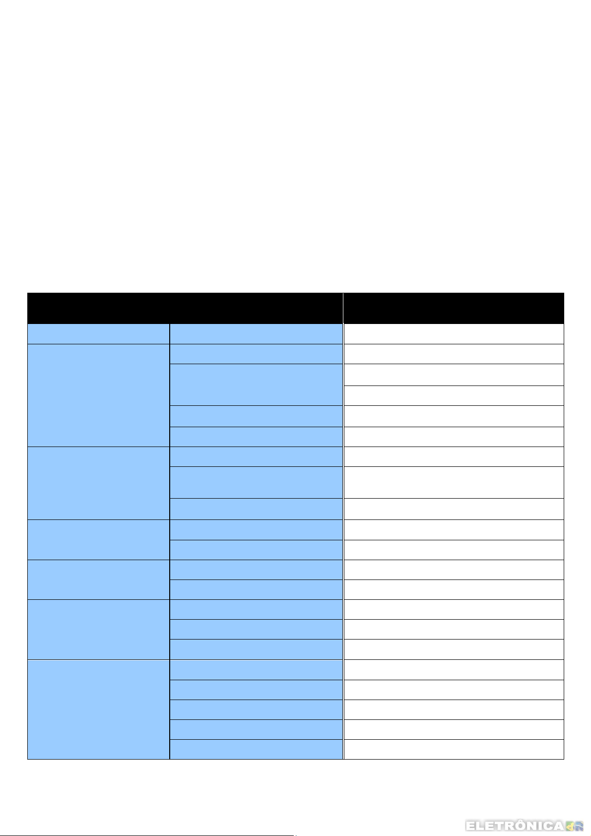
1.2 MS-1637 Product Specification (965GM-UMA + ICH8-M )
Item
Model
CPU Processor Type
Support Processor @ Launch
L2 Cache
FSB Speed
Socket
Memory Technology
Memory
(Max.)
CoreChip North Bridge
South Bridge
Display LCD Type
Brightness
Video Controller
VRAM
LCD
Audio Sound Controller
Spindle
H/W Spec
2
PBGA 478pin
Core™ DUO for Santa Rosa
2M/4M
667/800 MHz
PBGA 478pin
DDR II 533/667/800Mhz SDRAM
DDR II SO-DIMM X 2 slot
256/512/1024/2048 MB
2GB (2G DDR II SO-DIMM x 2)
GL965GM
ICH8-M (82801HBM)
15.4" WXGA Glare/ Non-glare
Brightness controlled by K/B hot-keys
GL965 (GMA X3100)
Sharing system memory
1280x800 for WXGA
Embedded in South Bridge
Sound Codec chip Realtek ALC883
Internal Speaker
Internal Microphone Yes
Sound Volume
2
2 Speakers, 1.5W
Adjust by volume button, K/B hot-key & SW
Page 4
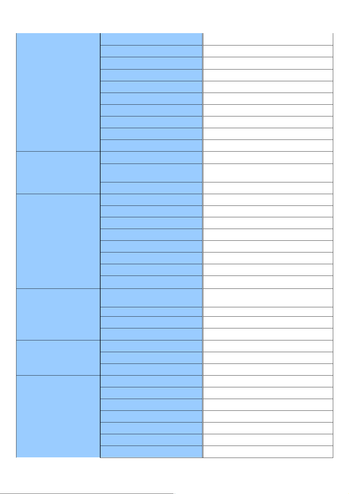
Communication Port
PCMCIA
56K Fax/MODEM
I/F
MDC1.5 (Azalia)
AZALIA S/W Modem
Controller AZALIA Embedded
Wake on Ring Support on S1/S2/S3 state
LAN Giga LAN 10/100/1000
LAN Controller Realtek RTL811B
Wake on LAN Support on S3/S4/S5 state
LAN Boot Yes
Blue Tooth MS-6837D, Bluetooth 2.0
Wireless LAN IEEE802.11A/B/G/N, MSI 6877/Kedron
Controller O2 OZ711SP
Care Reader MMC/SD/MS Pro 3 in 1 card reader x 1
I/O
Storage
Keyboard
Hot Keys
Card Bus Type II x 1
D-Sub x 1
USB 2.0 x 4
IEEE1394 x 1
Mic-in x 1
RJ11 x 1
RJ45 x 1
S-Video x 1
Headphone / SPDIF out x 1
HDD form factor
2.5" 9.5mm High, SATA 150, S.M.A.R.T,
5400~7200 rpm
HDD Capacity from 60GB to latest perpendicular capacity
IDE Controller ICH8-M
Optical Bay Combo, DVD-Dual+R9
Controller ENE 3910
MS Standard key code Support
Number of Keys 103 Keys
Dual Display Fn + F2
Touch Pad Disable/enable Fn + F3
LCD brightness / Down Fn + F4
LCD brightness / UP Fn + F5
Speaker Volume / Down Fn + F7
Speaker Volume / up Fn + F8
Speaker ON/OFF Fn + F9
3
Page 5
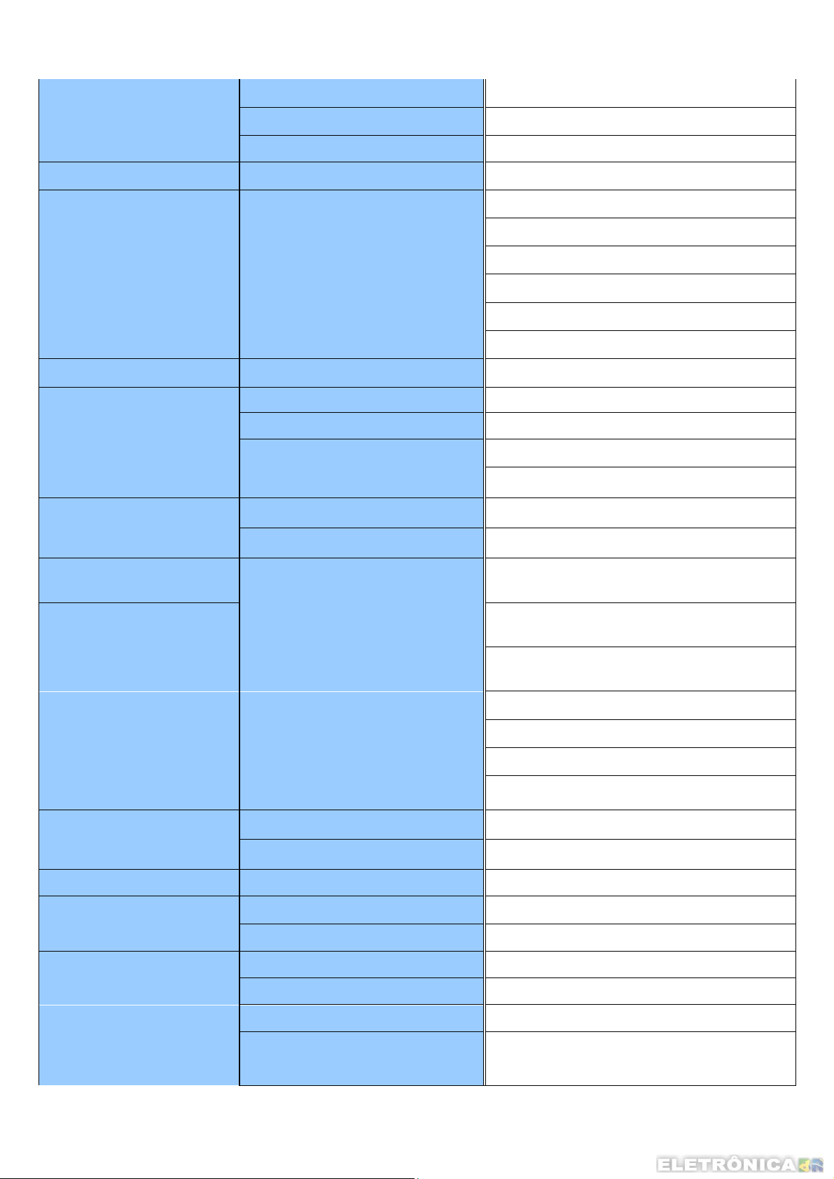
Feature
Launch Keys
Pointing Device
Camera enable Fn + F10
Bluetooth disable Fn + F11
Sleep Button Fn + F12
Camera Module Yes
Lunch Keys 4 Keys
-Power
-E_Mail
-Internet Explorer
-Bluetooth/WLAN
-P1
Glide Elantech with 2 buttons (click x 2)
Power AC adapter
1st Battery 6 cells(Li-ion) (2200mAh x2)
1st Battery Life
RTC Battery
65W
3 hrs, Battery Mark
Yes , 3 yrs
Security Features Kensington Lock Hole
HDD password
Status Indicator Indicator
Support (x1)
BIOS setting
- Power Status / suspend (Visible when LCD
module closed)
- HDD Status
- Battery Status (Visible when LCD module
closed)
- Num Lock
- Caps Lock
- Scroll Lock
-Wireless/ Bluetooth LAN on/off (visible when
LCD module closed)
Physical Characteristics Dimension
Weight
Compliance WHQL
Software Support OS
USB Flash boot
BIOS Fast Boot Support
OSD for Fn
VISTA capable
358 (W) x 259 (D) x 27-33(H) mm
2.8 Kg with 6 cell Battery
Win XP, Vista
Win XP, Vista
Yes, USB floppy boot up DOS only
Yes
SCM
Yes
Tool for splash screen customization
(post logo)
Yes
4
Page 6
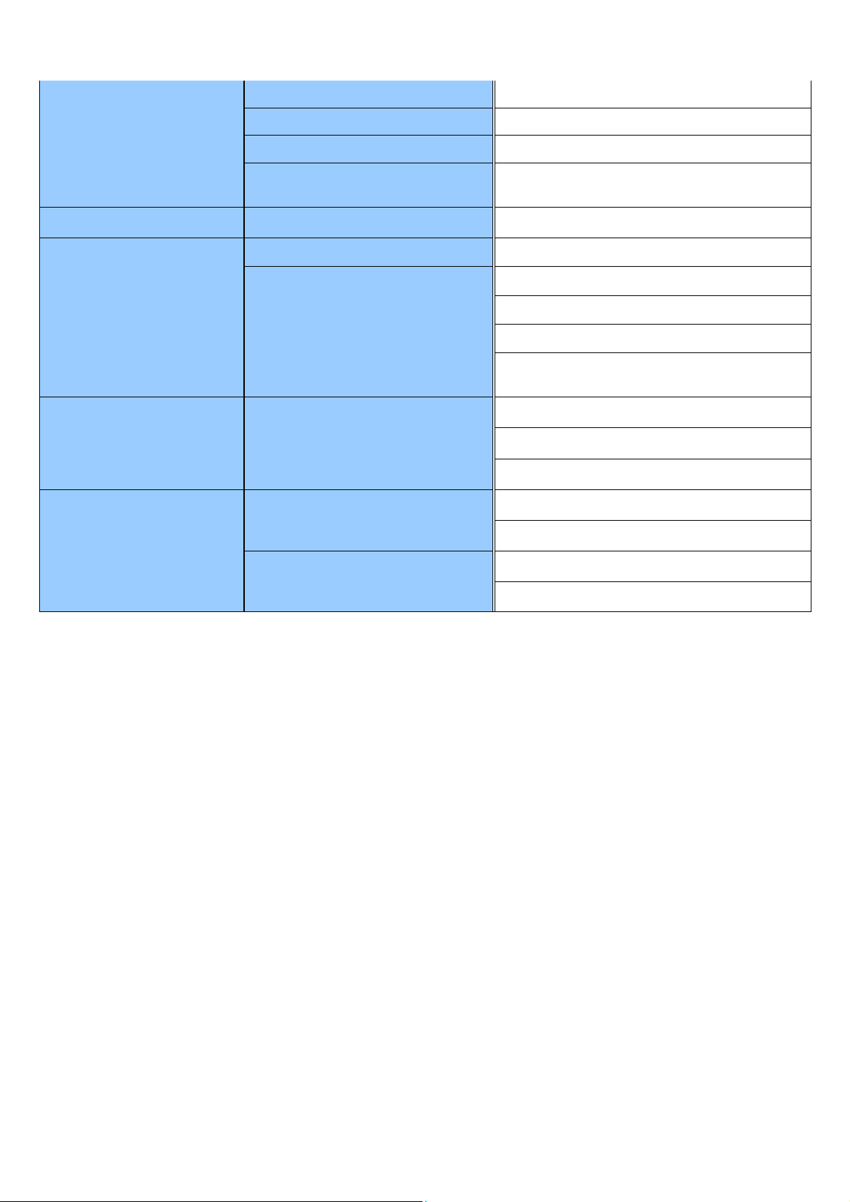
Boot form USB
Disable / enable Wireless LAN
Disable / enable all device boots
Disable / enable SMART functionality
for HDD
Yes
Yes
Yes
Yes
Power Management
ACPI for Vista Capability Yes
EMC EMS
EMI
Safety Safety
RF
Telecomm.
CE Mark (Europe)
FCC Class B Certified (USA & Canada)
BSMI (Taiwan)
CE Mark / Ctick
CCC (PRC)
UL, CSA (CUL) (USA & Canada)
TUV(Germany)
TUV-CB Report, CE-LVD Report(Europe)
USA, Canada, Taiwan, China,
Europe (Germany, France, Italy, Spain, UK)
FCC Part 68 (USA & Canada)
CTR 21 (Europe), JATE (Japan)
5
Page 7
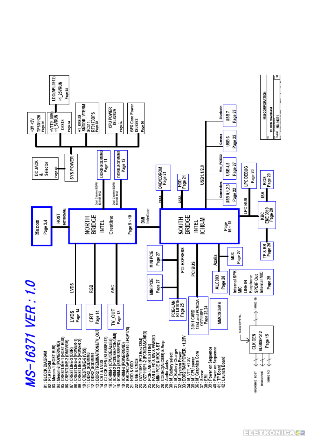
2、System Architecture
2.1 Block Diagram
6
Page 8
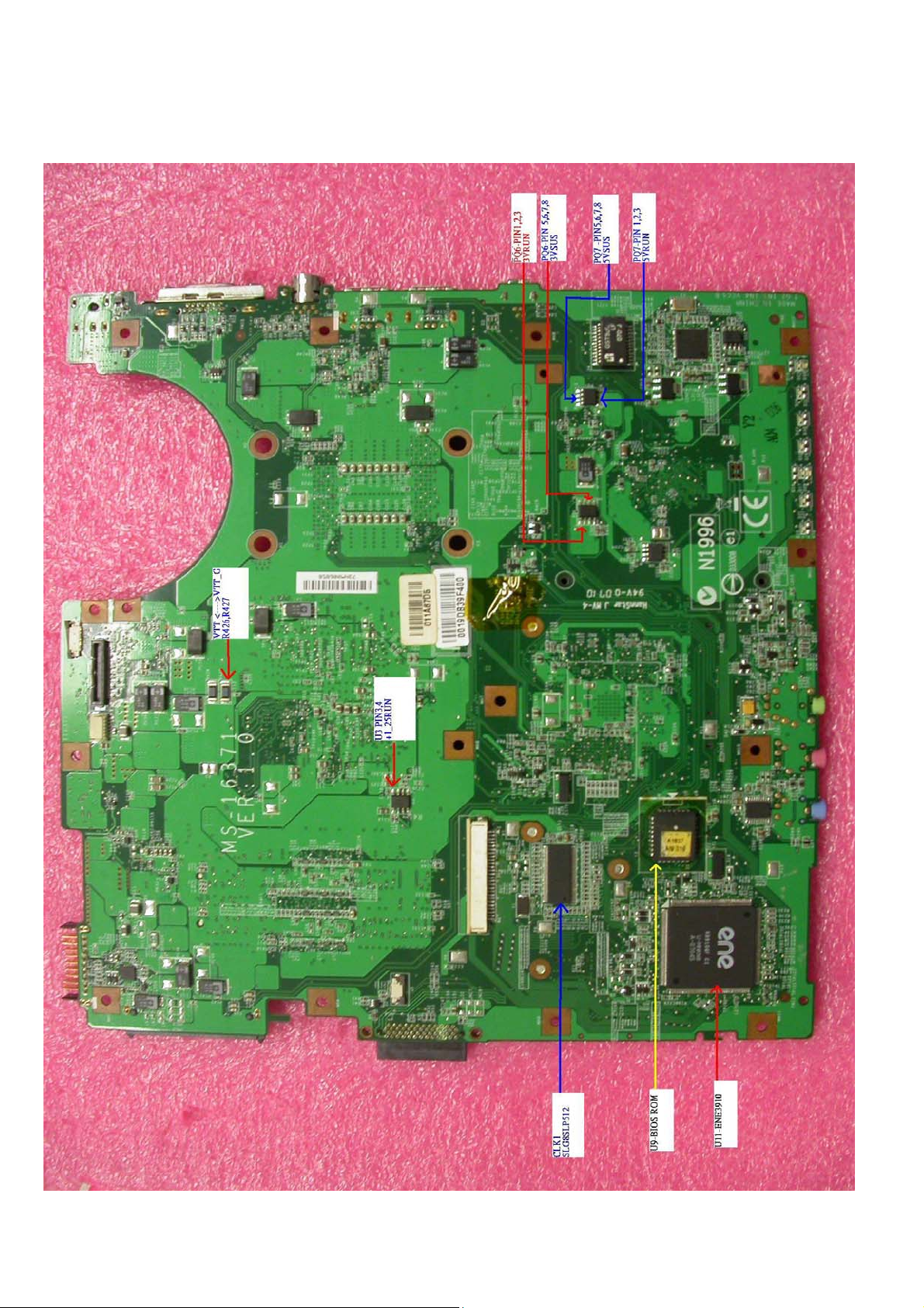
2.2 PCB Assembly Description
Top View
7
Page 9
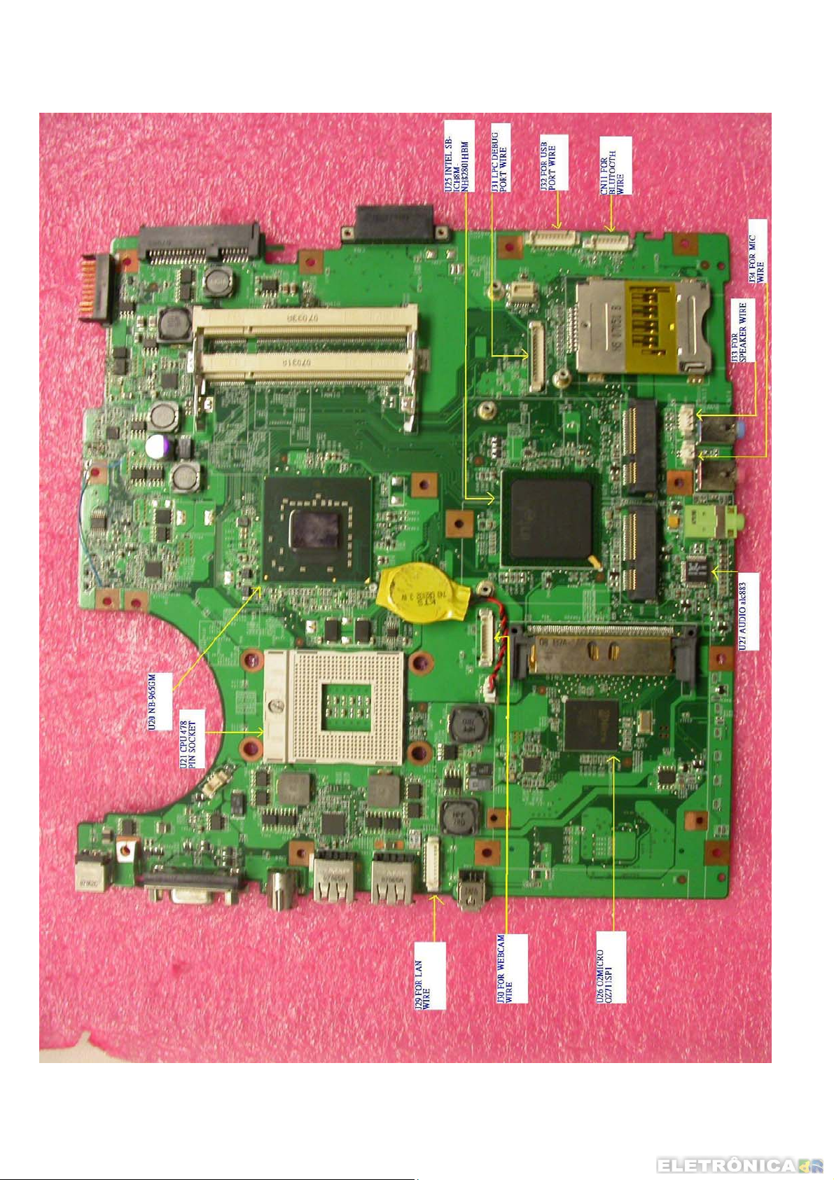
Bottom View
8
Page 10
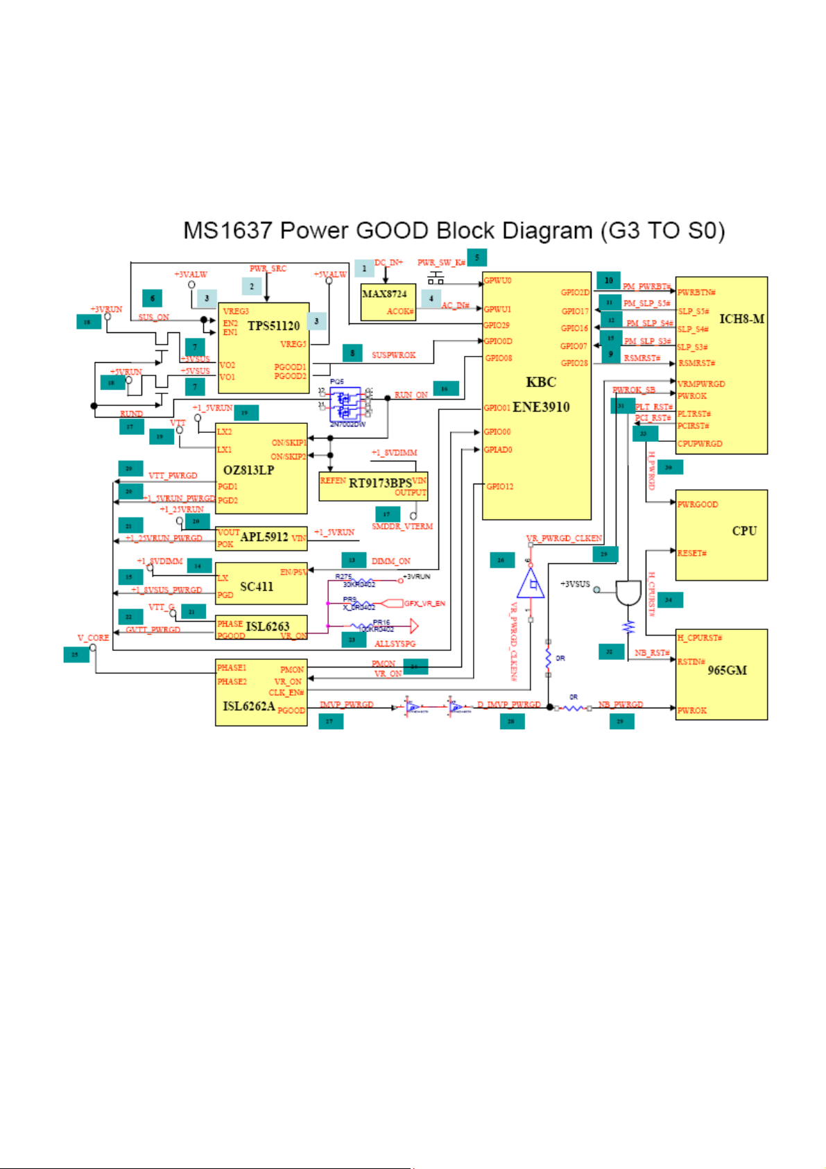
3、Power Map & Repair Flow Chart
3.1、POWER MAP
9
Page 11
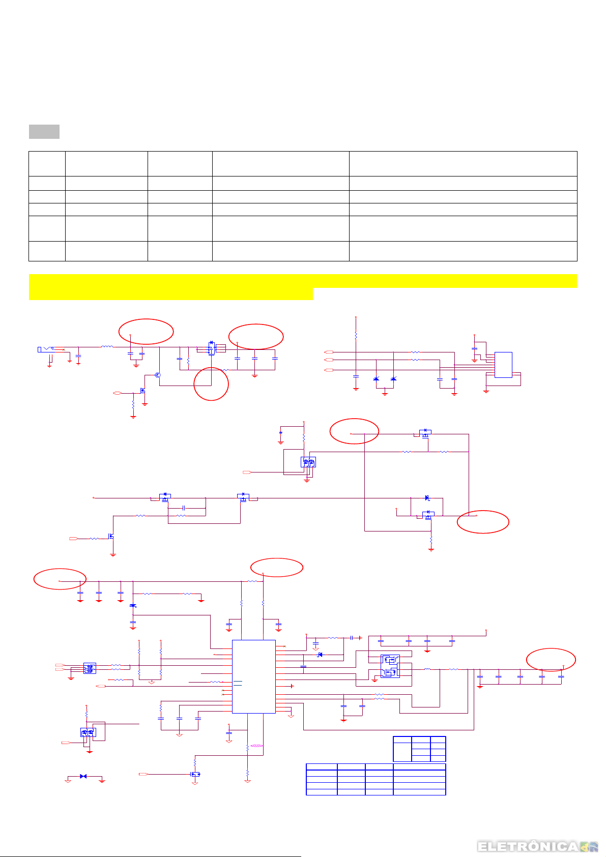
3.2 Repair Flow Chart
Debug by power sequence(Only insert adapter):
Please follow below step to check power source
Step 1、MAIN Power(PWR_SRC)
Item Name Description Check Component
Note
(related signal)
1-1 DC_PWR DC19V
PJ1、PQ11
1-2 DC_IN+ DC19V PQ11
1-3 SDC_IN+ DC19V PR74
1-4 V_CHG DC0V PU4(pin16) When battery charge, the voltage value is
DC12.6V
1-5 PWR_SRC DC19V PQ8
Note 1:It is recommendation to check the PWR_SRC (Power) first. If the power is right, you can check the next step
directly. If the power is fault, please check the related signal.
DCJACK_5
PWR-JACK3P_black-5.2mm
PJ1
1
2
3
4
5
ENCHG20,31
2、DC19V
DC_IN+
3S2P: Charge current set 3 Amp
3S3P: Charge current set 4.5 Amp
Pre-charger: Charge current set
220mA
PRE_CHG20
ENCHG_2P20
2N7002DW_SOT363
ENCHG20,30
G2S2D2
G1
S1
2N7002DW
+5VALW
PQ4
JT1X_NC
PFL1
1 2
CB-4532ES-121W
CI50
C0.1U50Y
AC_CTL20
V_CHG
PR81
2KR0402
Adapter= 90 W
Adapter input voltage set 17.4 Voltage
If <17.4V, ACOK#=high
PC81
PC77
0.1u_0603
2200p_0402X7R
PQ18
D1
+3VALW
AC_IN#20,30
PR32
10KR_0402
D1
D2
S2
S1
G2
G1
DS
PR105
499R_0402
19.1K_0402
PR108
PR26
100KR0402
PQ10
2N7002G
PR110
10KR_0402
MAX8724_ICTL
65W_DETEC16
DC_PWR
PC88
1、DC19V
PC1
PC72
X_C2200P50X0402
X_C0.1U50Y
E
B
C
DS
PQ3
2N7002
G
I=8A
Diode :
PP-AO4805_SO8
PQ9A
Is=2.6A
8
PR76 10KR0402
(Vref/2)/(PR109*(PR112+PR109))
2.048/7.15*(53.6+7.15)=17.4V
PR112
MAX8724_ACIN
53.6KR1%_0603
AC
PD9
10u_1206X6S
S-RB751V-40
PC105
1u_0805X7R
MAX8724_REFIN
MAX8724_LDO
PR111
10.5K_0402
PR30
95.3K_0402
PR102
1KR1%_0402
PC32
0.1u_0603
need to check value
65W_DETEC
65W_DETEC : DEFAULT=HIGH
High =>65W
Low =>90W
PC8
0.47U25Y0805
PQ2
P-DTA114EKA_SOT23
17
2
PC83 C0.1U25Y
PR78 100KR0402
PR109
7.15KR1%_0402
PR34
768R_0402
PR35
1.1K_0402
MAX8724_CCV
0.01u_0603X7R
X_40.2K_0402 1%
Diode :
Is=4.2A
PR6
240KR0402
MAX8724_REFIN
MAX8724_LDO
MAX8724_CCI
PC31
PR159
G
1
2
3
DC3.1V
MAX8724_LDO
MAX8724_ICTL
MAX8724_ACIN
MAX8724_CCS
PC28
0.01u_0603X7R
DS
Q28
I=15A
PQ11
P-AO4413_SOIC8
4
CHG_BATT_N
10KR_0402
X_2N7002
8
7
6
5
PR17
47KR0402
Diode :
Is=2.6A
PC99
0.1u_0603
PR107
MAX8724_REF
16.9KR1%_0402
DC_IN+
AC_IN#20,31
3 5
PU4
1
DCIN
15
VCTL
12
REFIN
13
ICTL
10
ACIN
8
SHDN
11
ACOK
9
ICHG
28
IINP
7
CCV
6
CCI
5
CCS
PC22
1u_0603
PR97
PR23
19.1K_0402 1%
2、DC19V
PC102
0.01U50X
I=8A
PQ9B
PP-AO4805_SO8
6
4
PR74
0.01R_3720
PR82
10R_0603
27
CSSP
4
0C
SET Iin MAX = A
PC107
0.1U50Y
3、DC19V
SDC_IN+
PR83
10R_0603
PC100
0.1u_0603
26
CSSN
CELLS
LDO
BST
DLOV
DHI
LX
DLO
PGND
CSIP
CSIN
BATT
GND
GND
CLS3REF
MAX8724ETI
PC36
10U25X1210
+3VALW
C4
1U10X
AC_OK
D2
S2
G2
CELL GND= 2 CELLS
FLOAT=3 CELLS
REFIN=4 CELLS
MAX8724_LDO
17
MAX8724_LDO
2
24
22
25
23
21
20
CSIP
19
CSIN
18
16
14
29
BATCLK_M20
BATDATA_M20
BAT_IN#20
PR15
100KR0402
D1
PQ1
2N7002DW
S1
G1
PR22
PC19
1u_0603
PD10
S-RB751V-40
PC103
0.1u_0603
Iinput=(Vcls/Vref)*(0.075/RS1)
RS1=PR74=0.01, Vref=4.096V
Vcls=4.096*PR23/(PR23+PR97)=2.29V
Iinput=(2.29/4.096)*(0.075/0.01)=4.2A
ENCHG-2P
01
0
0
100KR0402
PC4
X_0.1U25X
3、DC19V
SDC_IN+
33R_0603
AC
PR1
BATCLK_M
BATDATA_M
PRE_CHG
PC104
1UF_0603
PC110
0.1u_0603
1
01
0
0
+3VALW
PD1
ROHM ( UDZ3.3B )
PC115
0.1u_0603
A C
PQ14
2
3
4
NN-SP8K10S_SO8_0
PR95
10R_0603
PR96
10R_0603
ENCHG
1
1
0
PR3 100R0402
PR2 100R0402
PD3
ROHM ( UDZ3.3B )
A C
Diode :
Is=2.6A
PR7 10KR0402
VBATA
Diode :
Is=2.6A
PC95
2200p_0402X7R
81
7
6
5
PR23
Pre-charge
3S2P-Fast charge
3S3P-Fast charge
STOP CHARGE
X_10P50N0402
I=8A
PQ8A
PP-AO4805_SO8
8
Diode :
Is=3A
A C
ES3BB_DO214AA
6
PC7
0.1u_0603
CH-10U5A_S
PR97
28.7K
16.9K
I=8A
PL5
PC2
2
PD8
17
4
PC90
10U_25V_1206
65W
75W19.1K 24K
90W
PR4 100KR0402
35
PQ8B
PP-AO4805_SO8
PR80
470KR0402
PC13
10u_1210X5R
PR24
0.015R1%
VBATA
N91-09M0011-A10
CONN_BATTERY_2MM
PWR-1X8_black-NB
PC78
1
0.1U25X
PC3
X_10P50N0402
Pack+
0A
2
Pack+
3
CNT1
4
CNT2
5
CLK
6
DATA
7
THRM
8
10
Pack-
GND
9
11
Pack-
GND
CN1
PWR_SRC
PWR_SRC
5、DC19V
SDC_IN+
4、DC0V
PC98
10u_1210X5R
PC91
10u_1210X5R
PC119
0.1u_0603
Icharge=(Victl/Vrefin)*(0.075/RS2)
RS2=PR24=0.015
Vrefin=MAX8724_LDO*PR35/(PR34+PR35)
=5.4V*1.1K/(1.1K+768)=3.18V=MAX8724_REFIN
Victl=MAX8724_REFIN*PR30/(PR11+PR30)
For 3S2P:
Victl=3.18*(PR30//PR108)/((PR30//PR108)+PR11)
=3.18*15.91K/(15.91K+10.5K)=1.92V
Icharge=(1.92/3.18)*(0.075/0.015)=3.01A
For 3S2P:
Victl=3.18*PR30/(PR30+PR11)
=3.18*95.3K/(95.3K+10.5K)=2.86V
Icharge=(2.86/3.18)*(0.075/0.015)=4.5A
For Precharge:
Victl=3.18*(PR30//PR105)/((PR30//PR105)+PR11)
=3.18*0.496/(0.496+10.5K)=0.15mV
Icharge=(0.15mV/3.18)*(0.075/0.015)=0.236mA
PC9
10U_25V_1206
X_10U_25V_1206
V_CHG
PC14
10
Page 12
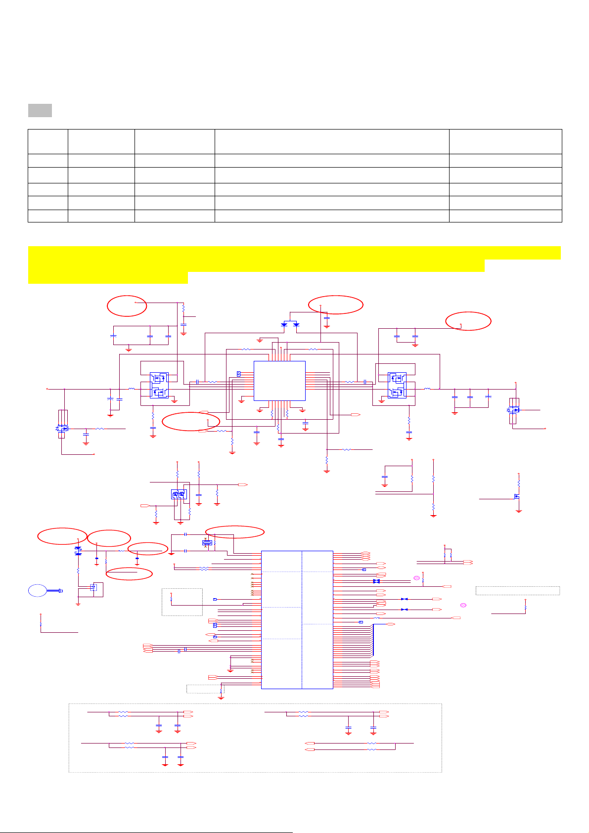
Step 2、3VALW & 5VALW & RTCVCC
Item Name Description Check Component
Note
(related signal)
2-1 +5VALW DC5V PU7-pin21(+5VALW)
2-2 +3VALW DC3.3V PU7-pin19(+3VALW)
2-3 RTCVCC DC3.3V DT1(RTC Power)
2-4 RTCRST
L>H(DC3.3V)
R340&C392
2-5 Y2 32.768KHZ
Note 1:It is recommendation to check the +5VALW、+3VALW、RTCVCC(Power) & Y2 (clock) first. If these power are
right, you can check the next step directly. If these signals are fault, please check the related signal.
Note 2: The L > H signal is H level.
Current limit at 6A for +3VSUS
Imax at 5A
+3VSUS
2、DC3.3V
BAT1
RTC_BAT
+3VRUN
N-AO4468_SOIC8
S-BAT54C_SOT23
R419
8.2KR0402
65W_DETEC
PQ6
876
4
2
351
+3VALW
2
DT1
1
D_P1
R82
1KR0402
RTC_P3
PC65
220U6.3S
R416 33K
C500
0.1u_0603
+3VRUN
3、DC3.3V
RTCVCC
3
C155
1U10X
4
1
2
3
HDA_SYNC
HDA_BIT_CLK_ICH8
12
R70
1MR0402
CN9
BH1X2S_white-1.25pitch
N32-1020290-H06
53398_02
PWR_SRC
DC19V
12
PC160
+
15U25S
CH-7U7. 2A_S
+
PC67
0.1U16X
RUND
RUN_ON9,20,33,34
R340
20KR0402
SM_INTRUDER#
4、L > H
SATA_RXN021
SATA_RXP021
SATA_TXN021
SATA_TXP021
R161 33R0402
R165 33R0402
R145 33R0402
R143 33R0402
PC159
.1U50Y
NN-SP8K10S
PL12
4、L > H
RTCRST#
C392
1U10X
PC158
2200P50X0402
PQ30
8 1
7
6
5
RI3
X_2.2R1%
CI90
X_1n_0402
RUND#
PQ5
2N7002DW
PR50
100KR
C189
X_33P50N0402
PR148
4.7R
VIN
PC163
1u_0805
PC166
0.1u_0603
2
3
4
3VSUSPK26
2、DC3.3V
SUS_ON20 ,26
PWR_SRCPWR_SRC
PR52
100KR
D1
D2
S2
S1
G2
G1
PR54
100KR
C171 18P50N0402
32K-12.5pf-S
C169 18P50N0402
RTCVCC
+1_5VRUN
R115
24.9R1%0402
Within 0.5" with
10mils Trace
CODEC_HDA_SDIN028
HDA_SDIN127
65W_DETEC31
SATA_ACTIVE#21
C28 3900P50X
C27 3900P50X
CLK_PCIE_SATA#15
CLK_PCIE_SATA15
Trace <0.5"
CODEC_HDA_SYNC 28
MDC_H DA_SY NC 27
C187
X_33P50N0402
C183
C181
X_33P50N0402
X_33P50N0402
PR158 0R0402
TP71
TP67
PR151
4.7R
LL2
3VSUSPK
+3VALW
100mA
1 2
PR155
2KR0402
1 2
PR51
47K
RUND
PR53
470KR
PC60
0.1u_0603
5、32.768KHZ
Y2
R116
10MR1%0402
2 3
1 4
RTCRST#
SM_INTRUDER#
ICH_INTVRMEN
R100330K
LAN100_SLP
R103330K
GLAN_DOCK#
TP112
GLAN_COMPI
HDA_BIT_CLK_ICH 8
HDA_SYNC
HDA_RST#
HDA_SDIN2
HDA_SDIN3
TP73
TP74
HDA_SDOUT
65W_DETEC
HDA_DOCK_RST#
TP72
SATA_ACTIVE#
SATA0TXN
SATA0TXP
SATARBIAS
R373
24R1%0402
CODEC_HDA_BITCLK 28
MDC_HDA_BIT_CLK 27
Place R close to ICH8 within 2"
10u_0805
PR153
100KR0402
RTCX1
RTCX2
V5FILT
PC164
10
11
12
13
14
15
16
33
RUND 28
PD6
RB717F_SOT323
9
EN5
EN3
PGOOD2
EN2
VBST2
DRVH2
LL2
DRVL2
GNDA
PR55
16.9K0402
U25A
AG25
RTCX1
AF24
RTCX2
AF23
RTCRST#
AD22
INTRUDER#
AF25
INTVRMEN
AD21
LAN100_SLP
B24
GLAN_CLK
D22
LAN_RSTSYNC
C21
LAN_RXD0
B21
LAN_RXD1
C22
LAN_RXD2
D21
LAN_TXD0
E20
LAN_TXD1
C20
LAN_TXD2
AH21
GLAN_DOCK#/GPI O13
D25
GLAN_COMPI
C25
GLAN_COMPO
AJ16
HDA_BIT_CLK
AJ15
HDA_SYNC
AE14
HDA_RST#
AJ17
HDA_SDIN0
AH17
HDA_SDIN1
AH15
HDA_SDIN2
AD13
HDA_SDIN3
AE13
HDA_SDOUT
AE10
HDA_DOCK_EN#/GPIO33
AG14
HDA_DOCK_RST#/GPIO34
AF10
SATALED#
AF6
SATA0RXN
AF5
SATA0RXP
AH5
SATA0TXN
AH6
SATA0TXP
AG3
SATA1RXN
AG4
SATA1RXP
AJ4
SATA1TXN
AJ3
SATA1TXP
AF2
SATA2RXN
AF1
SATA2RXP
AE4
SATA2TXN
AE3
SATA2TXP
AB7
SATA_CLKN
AC6
SATA_CLKP
AG1
SATARBIAS#
AG2
SATARBIAS
ICH8M_B0
HDA_SDOUT
VREF2
7
4
8
6
5
VO2
GND
VFB2
VREF2
COMP2
TPS51120RHBR
CS218PGND2
19
17
PC64
10u_0805
CODEC_HDA_RST#28
MDC_HDA_RST#27
1
3
4.7R0402
2
VFB1
COMP1
VIN
PR149
3
2
PR157 0R0402
1
VO1
SKIPSEL
TONSEL
PGOOD1
EN1
VBST1
DRVH1
LL1
DRVL1
PGND124CS123VIN22VREG521V5FILT20VREG3
PR56
13.7K0402
RTCLAN / GLAN
LPCCPU
CPUPWRGD/GPIO49
IHDA
IDE
SATA
R156 33R0402
R154 33R0402
100mA
+5VALW
PU7
SKIPSEL
32
TONSEL
31
5VSUSPK
30
29
28
27
26
25
PC63
1u_0603
FWH0/LAD0
FWH1/LAD1
FWH2/LAD2
FWH3/LAD3
FWH4/LFRAME#
LDRQ1#/GPIO23
A20GATE
DPRSTP#
STPCLK#
THRMTRI P#
DDACK#
CODEC_HDA_RST#
MDC_HDA_RST#
1、DC5V
PC162
1u_0603
PR150
PC165
4.7R
0.1u_0603
LL1
5VSUSPK 26
PR154
2KR0402
SUS_ON
1 2
PR152
100KR0402
1 2
LAD0
E5
LAD1
F5
LAD2
G8
LAD3
F6
C4
G9
LDRQ0#
LDRQ1#
A20M#
DPSLP#
FERR#
IGNNE#
RCIN#
DCS1#
DCS3#
DIOR#
DIOW#
IDEIRQ
IORDY
DDREQ
E6
AF13
AG26
AF26
AE26
AD24
AG29
AF27
AE24
INIT#
AC20
INTR
AH14
AD23
NMI
AG28
SMI#
AA24
AE27
AA23
TP8
V1
DD0
U2
DD1
V3
DD2
T1
DD3
V4
DD4
T5
DD5
AB2
DD6
T6
DD7
T3
DD8
R2
DD9
T4
DD10
V6
DD11
V5
DD12
U1
DD13
V2
DD14
U6
DD15
AA4
DA0
AA1
DA1
AB3
DA2
Y6
Y5
W4
W3
Y2
Y3
Y1
W5
TP85
DPRSTP#
R113 040212
DPSLP# H_DPSLP#
R102 040212
H_FERR#
INIT#
SMI#
THRMTRIP# PM_THRMTRIP#
R80 24. 9R1%0402
TP8
TP53
IDE_PDD0
IDE_PDD1
IDE_PDD2
IDE_PDD3
IDE_PDD4
IDE_PDD5
IDE_PDD6
IDE_PDD7
IDE_PDD8
IDE_PDD9
IDE_PDD10
IDE_PDD11
IDE_PDD12
IDE_PDD13
IDE_PDD14
IDE_PDD15
C184
X_33P50N0402
R158 33R0402
R159 33R0402
TONSEL
SKIPSEL
LAD0 20
LAD1 20
LAD2 20
LAD3 20
IDE_PDA0 21
IDE_PDA1 21
IDE_PDA2 21
IDE_PDCS1#21
IDE_PDCS3#21
IDE_PDIOR#21
IDE_PDIOW#21
IDE_PDDACK# 21
INT_IRQ1421
IDE_PDIORDY 21
IDE_PDDR EQ 21
C185
X_33P50N0402
PC156
.1U50Y
PQ31
NN-SP8K10S
2
3
4
Rds(on)Max23mR
RI2
X_2.2R_0603
CI84
X_1n_0402
PC66
1000p_0402X7R
LPC_FRAME# 20
L_LDRQ0# 20
H_A20GATE 20
H_A20M# 3
H_DPRSTP#
H_PWRGD 3
H_IGNNE# 3
R83 040212
H_INTR 3
KBRST# 20
H_NMI 3
R344 040212
H_STPCLK# 3
IDE_PDD[15:0] 21
CODEC_HDA_SDOUT 28
MDC_H DA_SDO UT 27
HDA_RST#
DC19V
PWR_SRC
PC157
2200P50X0402
Current limit at 6A for +5VSUS
PR156
X_0R_0402
0C
PL11
CH-7U7.2A_S
H_DPRSTP#
H_DPSLP#
VTT
R114
56R0402
Imax at 5A
PC61
0.1U16X
+5VALWVREF2
PR58
X_0R_0402
PR57
0R_0402
VTT
R112
R81
X_56R0402
X_56R0402
H_FERR# 3
H_INIT# 3
H_SMI# 3
12
PC62
PC161
+
10U10Y
220U6.3S
876
351
N-AO4468_SOIC8
RUND#
G
H_DPRSTP# 3,6,35
H_DPSLP#3
Place R close to ICH within 2"
0C
PM_THRMTRIP# 3,6
PM_THRMTRIP#
2
+3VRUN
+5VSUS
DS
PQ7
4
R64
X_47R0805
Q4
X_2N7002
VTT
RUND
R69
56R1%
+5VRUN
81
7
6
5
11
Page 13
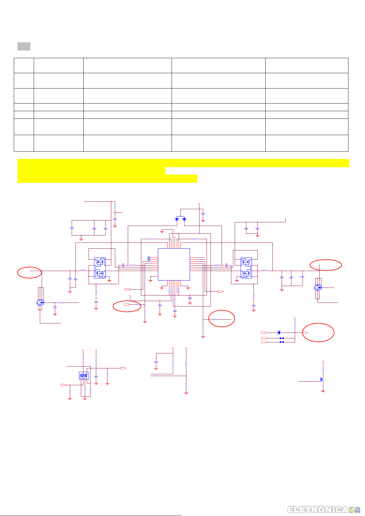
Step3、SUS Power
Item Name Description Check Component
Note
(related signal)
3-1 PWR_SW_K# Push bottom at least 100ms
J1-pin6 & U11-pin2
H > L( DC0V)
3-2 SUS_ON L > H(DC3.3V) U11-pin155& PR154& PR155
(+5VSUS & +3VSUS)
3-3 +5VSUS DC5V PQ7-pin5&PL11(+5VSUS)
3-4 +3VSUS DC3.3V PQ6-pin5&PL12(+3VSUS)
3-5 3V/5VSUSPK 3V/5V SUS Power OK
PU7-pin11&PU7-pin30
L > H(DC3.3V)
3-6 SUSPWROK SUS Power OK
U11-pin27&R183&R171
L > H(DC3.3V)
Note 1:It is recommendation to check the SUSPWROK first. If this signal is right, you can check the next step directly.
If this signal is fault, please check the related signal.
Note 2:The L > H signal is H level;The H > L signal is L level
Current limit at 6A for +3VSUS
Imax at 5A
+3VSUS
3.+3VSUS
876
2
351
N-AO4468_SOIC 8
PC65
220U6.3S
PQ6
R416 33K
4
C500
0.1u_0603
+3VRUN
RUN_ON9,20,33, 34
12
PC160
+
15U25S
12
+
PQ5
2N7002DW
PR50
100KR
PWR_SR C
CH-7U7.2A_S
PC67
0.1U16X
RUND
RUND#
PR148
4.7R
VIN
PC163
PC159
PC158
.1U50Y
2200P50X0402
PQ30
NN-SP8K10S
8 1
7
PL12
6
5
RI3
X_2.2R1%
CI90
X_1n_0402
PWR_SR CPWR_SR C
PR52
100KR
D1
D2
PC60
0.1u_0603
S2
S1
G2
G1
PR54
100KR
1u_0805
PC166
PR151
0.1u_0603
2
3
4
PR51
47K
RUND
PR53
470KR
4.7R
3VSUSPK26
+3VALW
100mA
SUS_ON20,26
1.SUS_ON
RUND 28
LL2
3VSUSPK
1 2
PR155
PR158 0R0402
9
TP71
EN5
10
TP67
EN3
11
PGOOD2
12
EN2
13
VBST2
14
DRVH2
15
LL2
16
DRVL2
33
GNDA
16.9K0402
V5FILT
PC164
10u_0805
PR153
100KR0402
1 2
PC66
1000p_0402X7R
TONS EL
SKIPSEL
PD6
RB717F_SOT323
8
VO2
TPS51120RHBR
17
PR55
PC64
10u_0805
1
VREF2
3
6
2
7
4
5
GND
VFB1
VFB2
VREF2
COMP2
CS218PGND2
19
VIN
PR149
4.7R0402
PR156
X_0R_0402
3
2
PR157 0R04 02
1
VO1
COMP1
SKIPSEL
TONS EL
PGOOD1
EN1
VBST1
DRVH1
LL1
DRVL1
PGND124CS123VIN22VREG521V5FILT20VREG3
PR56
13.7K0402
+5VALWVREF2
PR58
X_0R_0402
PR57
0R_0402
100mA
+5VALW
PC162
1u_0603
PC156
PC157
.1U50Y
2200P50X0402
PU7
SKIPSEL
32
TONS EL
31
5VSUSPK
30
29
28
27
26
25
PR150
PC165
4.7R
0.1u_0603
LL1
NN-SP8K10S
2
3
4
PQ31
81
7
PL11
CH-7U7.2A_S
6
5
Rds(on)Max23mR
PC63
1u_0603
PR152
100KR0402
1 2
PR154
2KR0402
SUS_ON
1 2
1.SUS_ON
5VSUSPK 26
X_2.2R_0603
X_1n_0402
RI2
CI84
5VSUSPK32
3VSUSPK32
PWR_SRC
Current limit at 6A for +5VSUS
Imax at 5A
+5VSUS
12
R182
100KR0402
PC62
10U10Y
+3VALW
+
PC161
220U6.3S
876
351
N-AO4468_SOIC 8
4.SUSPWROK
SUSPWROK 20SUS_ON20,32
RUND#
PC61
0.1U16X
AC
PD12 X_BAS40WS
R430 040212
R180 040212
2.+5VSUS
PQ7
4
2
+3VRUN
R64
X_47 R0 80 5
DS
Q4
X_2N7002
G
RUND
+5VRUN
12
Page 14
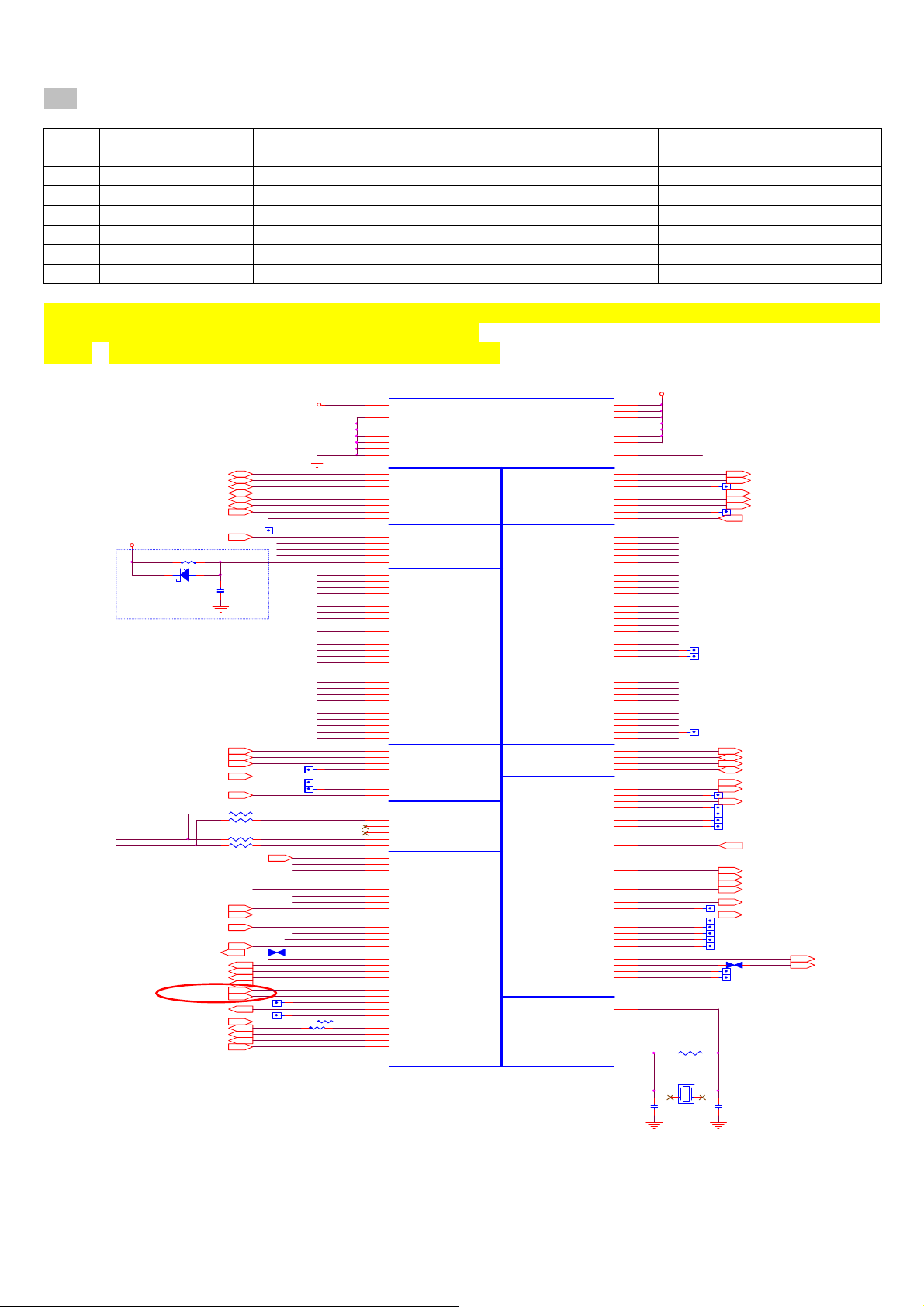
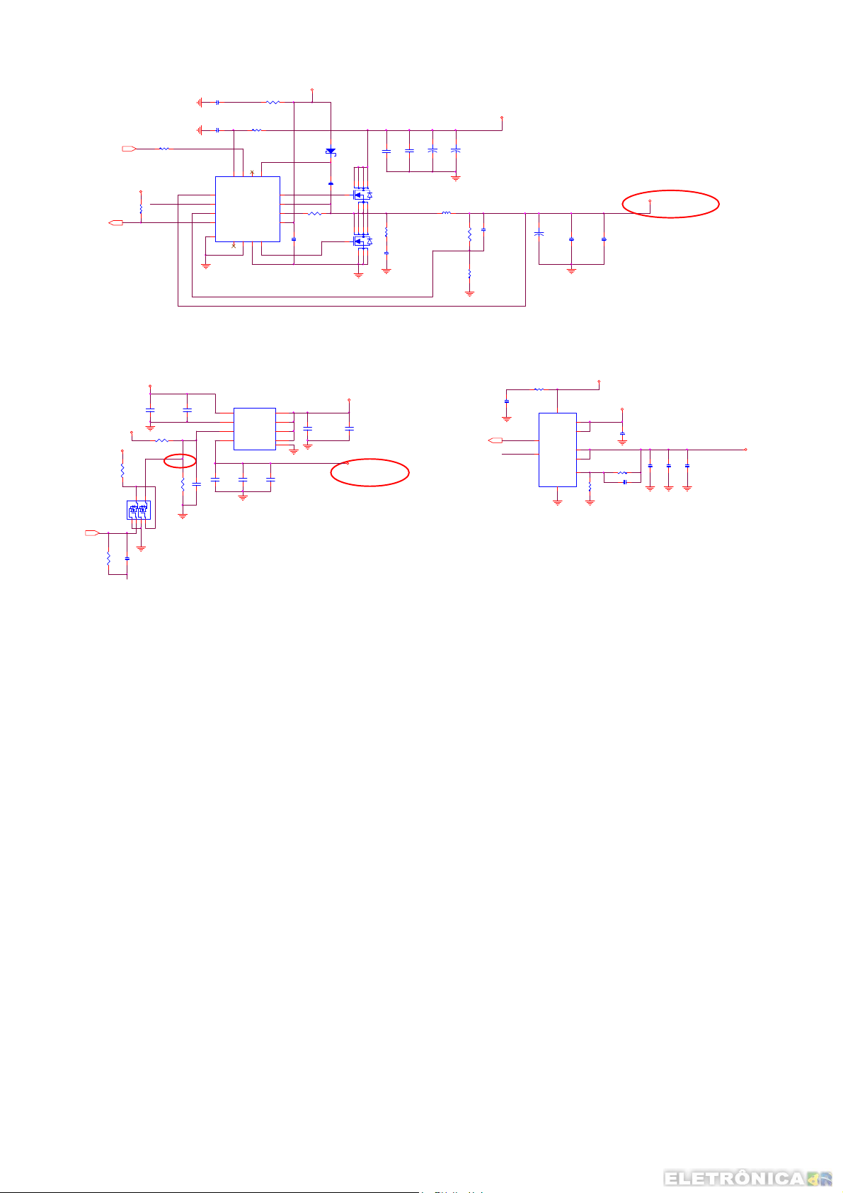
Step4、DDR2 Power
Item Name Description Check Component
Note
(related signal)
4-1 RSMRST# L > H(DC3.3V) U25-PinAG27,R208&R209
4-2 PM_PWRBTN# L > H(DC3.3V) U25-PinC2,D13
4-3 PM_SLP_S5# L > H(DC3.3V) U25-PinAD18,U11-pin75
4-4 PM_SLP_S4# L > H(DC3.3V) R126,U11-pin70
4-5 +1_8VDIMM DC1.8V PL8,PU1-pin1
4-6 SMDDR_VTERM DC0.9V PU5-pin4
Note 1:It is recommendation to check the SMDDR_VTERM first. If this signal is right, you can check the next step
directly. If this signal is fault, please check the related signal.
Note 2:The L > H signal is H level;The H > L signal is L level
+3VALW
PM_SLP_S4#
PM_SLP_S5#
LPC_FR AME#16
LPC_EC_CLK15
R168 10KR
D6
BAS40WS
Close to Pin19
PWR_SW_K#26
BT_WLAN_K#26
TP_CLK
TP_D ATA
CAMERA_K#26
SUSPWROK26
PM_SLP_S3#18,26
RUN_ON9,32,33,34
WLAN_PWRON#27
PM_SLP_S4#18
PM_SLP_S5#18
ENCHG_2P31
THERMAL_INT#26
CAMERA_KEY#22
U11
KBIN0
KBIN1
KBIN2
KBIN3
KBIN4
KBIN5
KBIN6
KBIN7
KBOUT0
KBOUT1
KBOUT2
KBOUT3
KBOUT4
KBOUT5
KBOUT6
KBOUT7
KBOUT8
KBOUT9
KBOUT10
KBOUT11
KBOUT12
KBOUT13
KBOUT14
KBOUT15
KBOUT16
KBOUT17
GPWU3
GPWU5
GPWU6
TP_CLK1
TP_DATA1
RUN_KBC
161
VCCBAT
17
GND
35
GND
46
GND
122
GND
137
GND
167
GND
159
BATGND
7
SERIRQ
9
LFRAME#
15
LAD0
14
LAD1
13
LAD2
10
LAD3
18
LCLK
25
CLKRUN #/GPIO0C
24
GPIO0B
165
LRST#/GPIO2C
6
KBRST#/GPIO03
5
GA20/GPIO02
31
ECSCI#
19
ECRST#
71
KSI0/GPIK0
72
KSI1/GPIK1
73
KSI2/GPIK2
74
KSI3/GPIK3
77
KSI4/GPIK4
78
KSI5/GPIK5
79
KSI6/GPIK6
80
KSI7/GPIK7
49
KSO0/GPOK0
50
KSO1/GPOK1
51
KSO2/GPOK2
52
KSO3/GPOK3
53
KSO4/GPOK4
56
KSO5/GPOK5
57
KSO6/GPOK6
58
KSO7/GPOK7
59
KSO8/GPOK8
60
KSO9/GPOK9
61
KSO10/GPOK10
64
KSO11/GPOK11
65
KSO12/GPOK12
66
KSO13/GPOK13
67
KSO14/GPOK14
68
KSO15/GPOK15
153
KSO16/GPOK16
154
KSO17/GPOK17
2
GPWU0
26
GPWU1
29
GPWU2
30
GPWU3
44
GPWU4
76
GPWU5
172
GPWU6/TIN1
176
GPWU7/TIN2/FANFB2
110
PSCLK1
111
PSDAT1
114
PSCLK2
115
PSDAT2
116
PSCLK3
117
PSDAT3
81
AD0/GPIAD 0
82
AD1/GPIAD 1
83
AD2/GPIAD 2
84
AD3/GPIAD 3
87
AD4/GPIAD 4
88
AD5/GPIAD 5
89
AD6/GPIAD 6
90
AD7/GPIAD 7
28
GPIO0E
27
GPIO0D
175
TOUT2/ GPI O2F
8
GPIO04
11
GPIO05/FAN 3PWM
12
GPIO06/FANFB3
20
GPIO07
21
GPIO08
22
GPIO09
48
GPIO10
62
GPIO13
63
GPIO14
69
GPIO15
70
GPIO16
75
GPIO17
109
GPIO24
118
GPIO25
119
GPIO26
148
GPIO27
149
GPIO28
155
GPIO29
156
GPIO2A
162
GPIO2B
168
GPIO2D
LPC
PS2 I/F
POWER & GND
KBC
ENE3910_C1_LQFP176
VCC
VCC
VCC
VCC
VCC
VCC
VCC
VCCA
AGND
XIO8CS#/GPIO18
XIO9CS#/GPIO19
XIOACS#/GPIO1A
XIOBCS#/GPIO1B
XIOCCS#/GPIO1C
XIODCS#/GPIO1D
XIOECS#/GPIO1E
XIOFCS#/GPIO1F
X-BUS
A20/GPIO23
RD#
WR#
IOCS#
MEMCS#
SCL1
SM-BUS
PWM2/GPOW2/FAN1PWM
PWM7/GPOW7/FAN2PWM
FANFB1/TOUT1/GPIO2E
CAPLOCK#/ GPIO11
SCROLLLOCK#/ GPIO0F
NUMLOCK#/GPIO0A
E51RXD/GPIO21/I SPCLK
E51TXD/GPIO22/ISPDAT
E51CS#/GPIO20/ ISPEN_TP
SDA1
SCL2
SDA2
PWM0/GPOW0
PWM1/GPOW1
PWM3/GPOW3
PWM4/GPOW4
PWM5/GPOW5
PWM6/GPOW6
FNLOCK#/ GPIO12
DA0/GPODA0
DA1/GPODA1
DA2/GPODA2
DA3/GPODA3
DA4/GPODA4
DA5/GPODA5
DA6/GPODA6
DA7/GPODA7
E51IT0/GPIO00
E51IT1/GPIO01
XCL KO
CLOCKS
XCL KI
A0
A1
A2
A3
A4
A5
A6
A7
A8
A9
A10
A11
A12
A13
A14
A15
A16
A17
A18
A19
D0
D1
D2
D3
D4
D5
D6
D7
18P50N0402
+3VALW
SIRQ18,23
LAD016
LAD116
LAD216
LAD316
LPC_RST#17
AC
C212
0.1U10X0402
AC_IN#30,31
BAT_IN#30
LID#14
IE_K#26
PRE_CH G31
ENCHG30, 31
AC_CTL30
RSMRST#18
SUS_ON26,32
MAIL_K#26
SIRQ
LPC_FRAME#
LAD0
LAD1
LAD2
LAD3 LED_WLAN#
LPC_EC_CLK
EC_CLKRUN#
TP91
TP100
TP98
X_0R0402R235
X_0R0402R236
0R0402R233
0R0402R234
PMON35
NB_THRM_ALERT#
LM86_THRM_ALERT#
12
TP103
TP102
KBC_GPIO0B
LPC_RST#
KB_RESET#
EC_A20GATE
KB_SCI#
EC_RST#
TP_CLK3
TP_DATA3
PMON
VBAT
ICHG
INP
3910P89
3910P90
KBC_RST#
HW_STRAP_11
HW_STRAP_12
X_0603
KB_SMI#
PRE_CHG
ENCHG
KBC_GPIO26
R211 0R
R208 100R0402
KB_PWRBT#
TP96
JNC19
16
34
45
123
136
157
166
95
96
85
86
91
92
93
94
97
98
124
125
126
127
128
131
132
133
143
142
135
134
130
129
121
120
113
112
104
103
108
138
139
140
141
144
145
146
147
150
151
152
173
163
164
169
170
32
33
36
37
38
39
40
43
171
54
55
41
23
99
100
101
102
1
42
47
174
3
4
106
107
105
160
EC_XIN
158
C258
+3VALW
EC_VCCA
EC_AGND
LED_BATLOW#
LED_CHARGE#
GPIO1A
LED_ACPI #
LED_BLUETOOTH#
KBC_GPIO1E
EC_A0
EC_A1
EC_A2
EC_A3
EC_A4
EC_A5
EC_A6
EC_A7
EC_A8
EC_A9
EC_A10
EC_A11
EC_A12
EC_A13
EC_A14
EC_A15
EC_A16
EC_A17
EC_A18
EC_A19
EC_A20
EC_D0
EC_D1
EC_D2
EC_D3
EC_D4
EC_D5
EC_D6
EC_D7
EC_RD#
EC_WR#
EC_CS#
MEM_CS #
BATCLK_M
BATDATA_M
SMB_CPU_CLK
SMB_CPU_DATA
GPOW2
GPOW4
GPOW5
GPOW6
GPOW7
FAN_TACH1
LED_CAP#
VR_ON
LED_SCR#
LED_NUM#
BR-AD-ADJ
DA3
DA4
DA5
DA6
DA7
ALLSYSPG
DI MM_ON _K BC
E51RXD
E51TXD
HW_STRAP_10
EC_XOUT
R204
10MR1%0402
YT1
1 4
2 3
32K-12.5pf -S
LED_BATLOW# 26
LED_CHARGE# 26
TP101
LED_ACPI# 26
LED_BLUETOOTH# 26
LED_WLAN# 26
TP121
KEY_101_87 18
RUN_ON is pulled low in P.33
TP123
TP105
TP99
BATCLK_M 30
BATDATA_M 30
SMB_CPU_CLK 26
SMB_CPU_DATA 26
CAMERA_ON 22
PCIE2_ON# 27
TP89
BT_PWR_ON# 27
TP93
TP87
TP92
TP90
FAN_TACH1 26
LED_CAP# 26
VR_ON 35
LED_SCR# 26
LED_NUM# 26
BR-AD-ADJ 14
TP120
FAN1_PWM 26
TP122
TP94
TP88
TP115
DIMM_ON is pulled low in P.34
TP97
JNC20
12
X_0603
TP106
TP104
C253
18P50N0402
ALLSYSPG 26
DIMM_ON 22,33
13
Page 15
+5VSUS
PR5
10R
SC411_VCCA
PC5
1U16Y0603
PR19
PC15
PR18
DIMM_ ON20,22
+3VSUS
PR8
+1_8VSUS_PWRGD26
X_100K0402
1K0402
SC411_VCCA
1000P50X0402
1
2
3
4
17
1M0402
PU1
14
16
13
15
NC
BST
VOUT
VCCA
FB
PGD
TPAD
TON
SC411
5
12
EN/PSV
DH
11
LX
10
ILIM
9
VDDP
DL
PGND
VSSA6NC
8
7
PC12
0.1U25Y 0402
PR10
7.15K1%0402
PQ20
FDS6676AS_SOI C8
Rds 6m
PC6
1U16Y0603
PD4
AC
S-RB751V-40
1 2
12
+
0.1U50Y
2200P50X0402
15U25VPOS
PC34
PC112
PC108
876
PQ19
4
N-AO4468_SOIC 8
2
351
876
PR113
4
X_3R
2
351
X_1000P50X0402
FOR EMI
PC123
PL8
CH-1.5U10A-RH
DCR 3.3m
26.7K1%0402
10K1%0402
PWR_SRC
Del PL2
12
+
X_15U25VPOS
PC30
Current limit at 11A for 1.8VSUS
Imax at 8.5A
PR13
PC10
X_10P50N0402
PR14
12
+
PC41
220u/2.5V
ESR 15m
PC42
2200P50X0402
PC11
0.1U10X0402
+1_8VD IMM
+1_8VDIMM
RUN_ON9,20,32,34
100KR0402
PR118
X_100KR0402
+5VSUS
PR121
PQ25
2N7002DW
1 2
+1_8VDIMM
1 2
S1
PC139
0.1U25Y 0402
1 2
D1
G1
+1_8VDIMM
PC129
10UF/10V_ 0805
1 2
PR115
33KR1%
DDR_ 0.9V
PR116
33KR1%
D2
S2
G2
PC131
0.1U/10V_04 02
1 2
1_8V_REFEN
PC132
0.1U10X0402
1
2
3
PC138
10U6.3X1206
PU5
VIN
VCNTL
GND
VCNTL
REFEN
VCNTL
OUTPUT4VCNTL
GND1
_RT9173BPS_SOIC8
PC137
10U6.3X1206
8
7
6
5
9
12
PC136
0.1U25Y 0603
PC135
0.1U/10V_040 2
SMDDR_VTERM
+5VSUS
PC130
4.7UF/ 10V_0805
DDR_ 0.9V
SMDDR_VTERM
R44
1KR0402
1V25_EN
C121
C0.1U16Y0402
+1_25VRUN_PWRGD26
1V25_EN
7
8
U3
APL5912
POK
EN
+5VRUN
5
9
4
3
2
R46
5.11KR1%0402
C130
C0.01U25X0402
R50
9.09KR1%0402
+1_5VRUN
APL5912 supply 5A MAX
Newcard spec. request 750mA
peak
C114
C10U10Y0805
+1_25VRUN
1.25V/1.5A
X_22U6.3X0805
C501
Vout=0.8*(1+(R46/R50))
=0.8*(1+(5.11K/9.09K))
=1.25V
22U6.3X0805
C120
C118
C0.1U16Y0402
6
VIN
VCNTL
VIN
VOUT
VOUT
FB
GND
1
14
Page 16
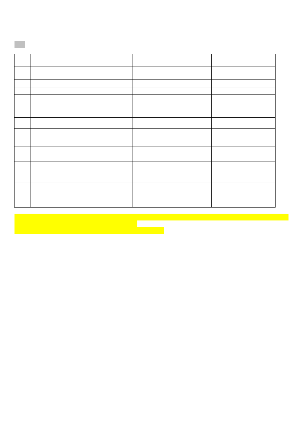
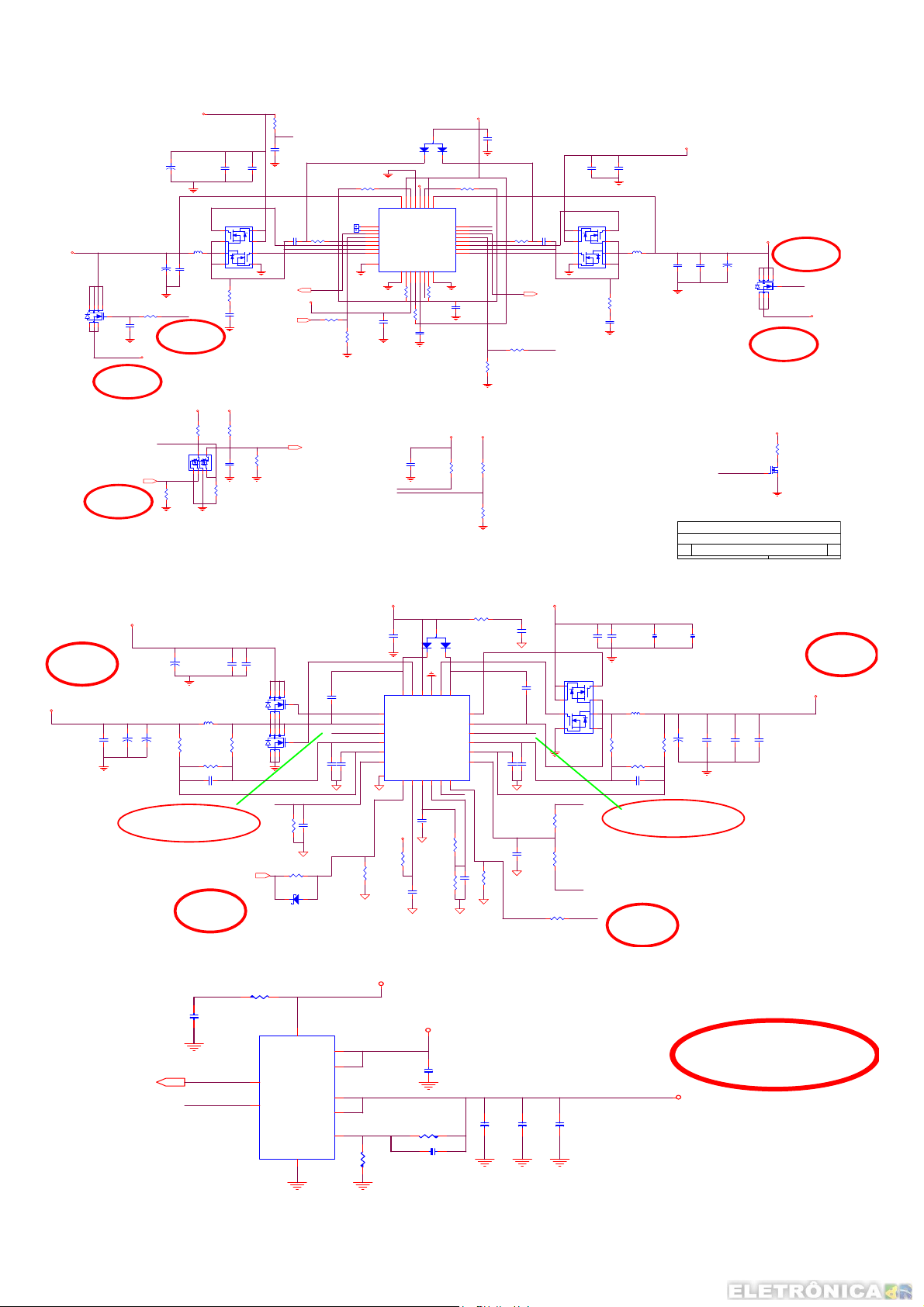
Step5、RUN POWER
Item Name Description Check Component
Note
(related signal)
5-1 PM_SLP_S3# L > H(DC3.3V) R125 (PM_SLP_S3#)
U11-pin20
5-2 RUN_ON L > H(DC3.3V) U11_PIN21(RUN_ON)
5-3 RUND DC 17.75V PR51(RUND)
5-4 VTT DC1.05V PL6(VTT)
5-5 +1_5VRUN DC1.5V PL4(+1_5VRUN)
5-6 +3VMCLK DC3.3V L26 CLK1(Clock Power)
5-7 +5V_AUDIO DC5V Q27 & U14,U27(Codec Power)
5-8 +1_25VRUN DC1.25V U3_PIN3,4(+1_25VRUN)
5-9 +3VRUN DC3.3V PQ6(+3VRUN)
5-10 +5VRUN DC5V PQ7(+5VRUN)
5-11 +1_5VRUN_PWRGD Power Good
L > H(DC3.3V)
5-12 VTT_PWRGD Power Good
L > H(DC3.3V)
5-13 ALLSYSPG ALL Power Good
L > H(DC3.3V)
PU2-pin21
(+1_5VRUN_PWRGD)
PU2-pin10
(VTT_PWRGD)
R2 ,U11-pin3
(ALLSYSPG)
Note 1:It is recommendation to check the ALLSYSPG first. If this signal is right, you can check the next step directly.
If this signal is fault, please check the related signal.
Note 2:The L > H signal is H level;The H > L signal is L level
15
Page 17
3V_5V RUN POWER
Current limit at 6A for +3VSUS
Imax at 5A
+3VSUS
PQ6
876
4
2
351
N-AO4468_SOIC8
PC65
220U6.3S
R416 33K
C500
0.1u_0603
+3VRUN
12
PC160
+
15U25S
12
+
2.RUND
PWR_SRC
RUND
PL12
CH-7U7.2A_S
PC67
0.1U16X
PC159
.1U50Y
NN-SP8K10S
8 1
7
6
5
3. +3VRUN
PWR_SRCPWR_SRC
PR52
100KR
RUND#
D1
D2
PQ5
2N7002DW
S2
S1
G2
RUN_ON9,20,33,34
1.RUN_ON
G1
PR50
100KR
PR54
100KR
VTT & 1.5V RUN POWER
PWR_SR C
12
PC111
12
PC38
+
220u/2.5S
+
22U25S
CH-1.5U10A_S-1
51R1%0402
PR70
PC79 C3300P50X0402
C0.1U25Y
PL6
PR73
100KR1%0402
PR71
162KR1%0402
PC89
2. VTT
Current limit at 10A for VTT(1.05)
Imax at 8.5A
VTT
Vout=Vref(105k)/(124k+44.2k+105k)
Vref=2.75V
Vout=1.05V
C1U16Y
PC35
PC37
X_220U2.5S
12
+
3. VTT_PWRGD
1. RUN_ON
+1.25V RUN
1V25_EN
C121
C0.1U16Y0402
+1_25VRUN_PWRGD26
1V25_EN
PC158
2200P50X0402
PQ30
RI3
X_2.2R1%
CI90
X_1n_0402
PR51
47K
PC60
0.1u_0603
PC93
C2200P50X0402
RUN_ON9,20,32,33
R44
1KR0402
7
8
U3
APL5912
2
3
4
RUND
PR53
470KR
876
2
351
N-AO4468_SOIC8
876
2
351
FDS6676AS_SO IC8
PR68
105KR1%
PR65 100KR_0402
POK
EN
PR148
4.7R
VIN
PC163
1u_0805
PC166
0.1u_0603
3VSUSPK26
100mA
SUS_ON20,26
2.RUND
RUND 28
I=?A
Diode :
Is=?A
PQ15
4
4
PQ13
813_CS1P
813_CS1N
D41 BAS40WS
6
VCNTL
GND
1
PD6
RB717F_SOT323
PR158 0R0402
7
8
6
VO2
VFB2
COMP2
9
TP71
EN5
TP67
10
EN3
PR151
4.7R
LL2
3VSUSPK
+3VALW
1 2
PR155
2KR0402
813_DL1
C22P50N0402
PC75
C1000P16X0402
AC
11
PGOOD2
12
EN2
13
TPS51120RHBR
VBST2
14
DRVH2
15
LL2
16
DRVL2
33
GNDA
CS218PGND2
19
17
PR55
16.9K0402
V5FILT
PC164
10u_0805
PR153
PC64
100KR0402
+5VSUS
PU2
12
HDR1
11
LX1
10
PGD1
9
CS1P
8
CS1N
7
VSET1
25
GNDA
PWR_SRC
PR62
1KR0402
PC71
C0.1U1 0X0603
10u_0805
TONSE L
SKIPSEL
PC87
C1U16Y
13
14
BST1
OZ813LP_QFN24
ON/SKIP1
6
2
1 2
PC85
C0.1U25Y
813_DH1
813_LX1 813_LX2
VTT_PWRGD
PC82
PC74
C4700P25X0402
PR60
0.1U10X0402
+5VRUN
+1_5VRUN
5
VIN
9
VIN
4
VOUT
3
VOUT
2
FB
R46
5.11KR1%0402
C130
C0.01U25X0402
R50
9.09KR1%0402
1
VREF2
2
4
3
5
GND
VFB1
VREF2
VIN
PR149
4.7R0402
PC66
1000p_0402X7R
2
16
LDR1
VDDP
VREF
3
813_VREF
PC69
C1U16Y
1KR1%0402
PR59
20KR1%0402
COMP1
15
4
100mA
+5VALW
3
2
PR157 0R0402
1
VO1
SKIPSEL
TONSE L
PGOOD1
EN1
VBST1
DRVH1
LL1
DRVL1
PGND124CS123VIN22VREG521V5FILT20VREG3
PR56
13.7K0402
3
1
17
LDR2
GNDP
TSET
VDDA5VIN
813_VDDA
PR64
C114
C10U10Y 0805
PC162
1u_0603
PU7
SKIPSEL
32
TONSE L
31
5VSUSPK
30
29
28
27
26
25
PC63
1u_0603
PR156
X_0R_0402
PR61
10R
PD2
S-RB717F_SOT323- RH
18
BST2
HDR2
LX2
PGD2
CS2P
CS2N
VSET2
ON/SKIP2
1
PC68
C1000P50X0402
PR150
PC165
4.7R
0.1u_0603
LL1
5VSUSPK 26
PR154
2KR0402
SUS_ON
1 2
PR152
100KR0402
1 2
+5VALWVREF2
PR58
X_0R_0402
PR57
0R_0402
PWR_SRC
813_VDDA
PC70
C1U16Y
813_DL2
PC86
C0.1U25Y
813_DH2
19
20
+1_5VRUN_PWRGD
21
PC84
22
23
PC76
C22P50N0402
C4700P25X0402
24
813_CS2P
813_CS2N
813_VSET2
PC73
C1000P16X0402
PR63
X_100KR0402
APL5912 supply 5A MAX
Newcard spec. request 750mA
peak
22U6.3X0805
C120
C118
C0.1U16Y0402
X_2.2R_0603
X_1n_0402
2
3
4
NN-SP8K10S_SO8_0
813_VREF813_VSET1
PR66
124KR1%
PR69
44.2KR1%0402
813_VSET1
PR67
0R_0402
PC156
.1U50Y
PQ31
NN-SP8K10S
2
3
4
Rds(on)Max23mR
RI2
CI84
PC97
C0.1U25Y
81
7
6
5
PQ12
RUN_ON
X_22U6. 3X0805
C501
PWR_SRC
PC157
2200P50X0402
Current limit at 6A for +5VSUS
81
7
6
5
Imax at 5A
PL11
CH-7U7.2A_S
PC92
C2200P50X0402
PL4
CH-2.5U 7.5A_S
PR72
51R1%0402
PR77
100KR1%0402
PR75
470KR0402
PC80
C3300P50X0402
PC61
PC62
0.1U16X
10U10Y
Title
SYSTEM POWER 3/5V
Size Document Number Rev
Cust om
MS-16371
Date: Sheet
PC25
PC26
C10U25X51206
C10U25X51206
Vout=Vref(105k+44.2k)/(124k+44.2k+105k)
Vref=2.75V
Vout=1.50V
Current limit at 6A for +1_5VRUN
Imax at 4.5A
12
PC124
+
C10U10Y 0805
220u/2.5V
3. +1_5VRUN_PWRGD
1. RUN_ON
2. +1_25VRUN
+1_25VRUN
1.25V/1.5A
Vout=0.8*(1+(R46/R50))
=0.8*(1+(5.11K/9.09K))
=1.25V
12
+
PC161
220U6.3S
N-AO4468_SOIC8
RUND#
MSI CORPORATION
PC125
PC126
C1U16Y
+5VSUS
2.RUND
PQ7
876
RUND
4
2
351
3. +5VRUN
+3VRUN
R64
X_47R0805
DS
Q4
X_2N7002
G
32 42Tuesday, F ebruary 27, 2007
PC127
C0.1U25Y
+5VRUN
0B
of
2.+1_5VRUN
+1_5VRUN
16
Page 18
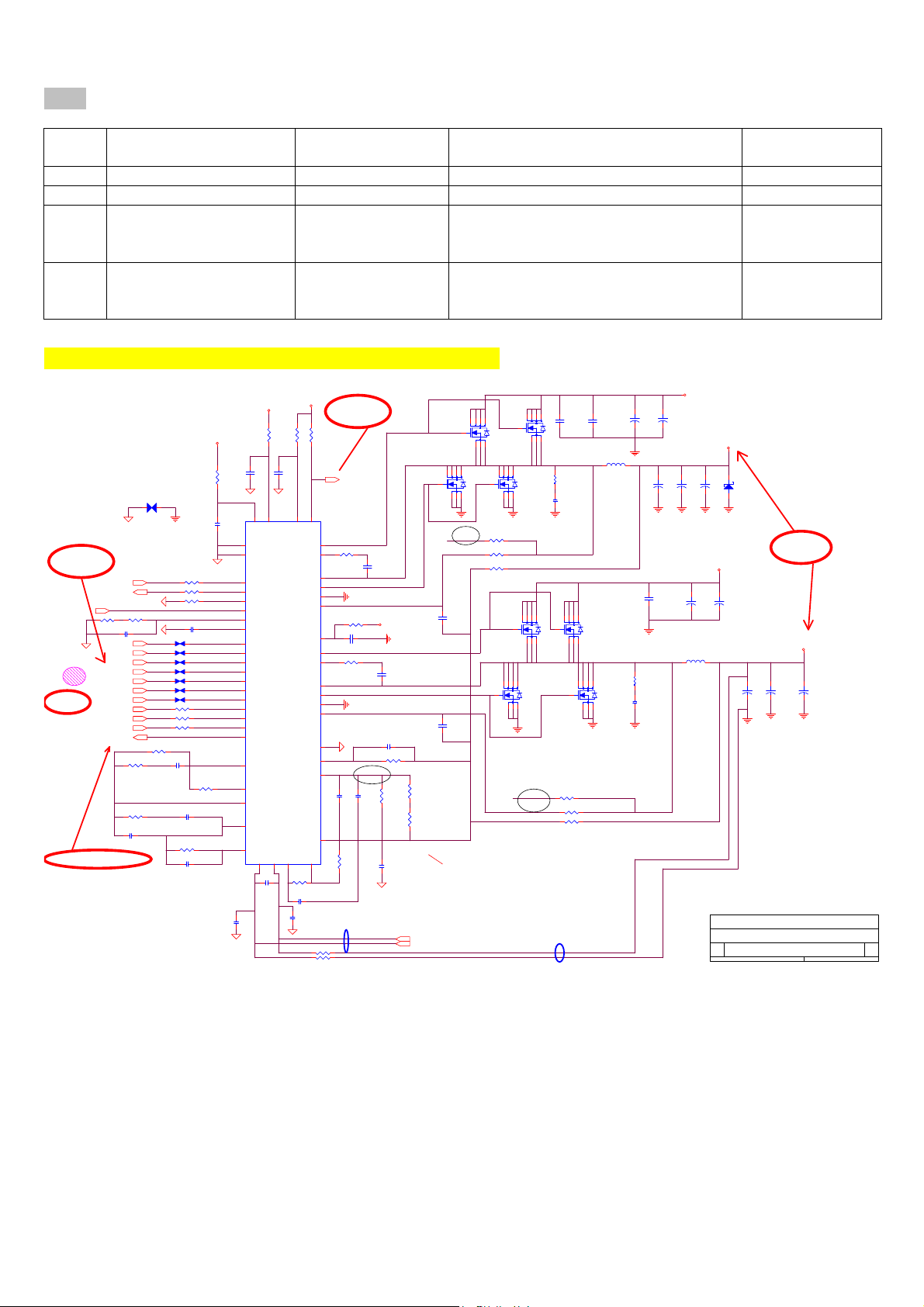
Step6、CPU Power
Item Name Description Check Component
(related signal)
6-1 VR_ON L > H(DC3.3V) U11-pin55 & PU6-pin44 (VR_ON)
6-2 V_CORE Control by VID[6:0] R88 & U25(CPU Power)
6-3 VR_PWRGD_CLKEN# H > L(DC0V) PU6-pin47 (D_VR_PWRGD_CLKEN#)
U24-pin1,6
(VR_PWRGD_CLKEN)
6-4 IMVP_PWRGD
PWROK
L > H(DC3.3V)
PU6-pin (IMVP_PWRGD)
U20_AW49/R287-PWROK&
U25_AE23/R101-PWROK
Note 1:The L > H signal is H level;The H > L signal is L level
VCORE_GND
2.CPU_VID
H_PROCHOT#3
PR138 4.02KR1%0402
0.01U25X0402
PC150
VCORE_GND
0C
1.VR_ON
4.VR_PWRGD_CLKEN#
CPU_VID04
CPU_VID14
CPU_VID24
CPU_VID34
CPU_VID44
CPU_VID54
CPU_VID64
PM_DPRSLPVR6, 18
H_DPRSTP#3,6, 16
VR_PWRGD _CLKEN#15,26
PSI#3
PMON20
VR_ON20
442R1%0402
PR131
J4 X_X
Throttling temp.
105 degree C
PR141 0R0402
PMON
PR140 X_0R0402
VCORE_GND
PR126
470KRT5%
PC53 0.015U16X0402
VCORE_GND
PR142 040212
PR143 040212
PR144 040212
PR145 040212
PR137 040212
PR136 040212
PR133 040212
PR132 0R0402
PR129 499R1%0402
PR130 0R0402
PR128
1.82KR1%0402
PC145
470P50X0402
PR135
180KR1%0402-1
PC50
120P50N
PR134 6.81KR1%04 02
PR40
10R
PR46
147KR1%
PR125
3.57KR1%0402
PC52
270P50N
PC148
1000P50X
0.01U25X0402
+5VRUN
VCORE_GND
PC141
VCORE_GND
PC49
C1U10X
21
49
37
38
39
40
41
42
43
44
45
46
47
13
12
11
10
VCORE_GND
2
3
4
5
6
7
9
PWR_SRC
PR39
10R
1 2
PC143
22
VDD
ISL6262A_MLFP_48
GND
GND_T
PSI#
PMON
RBIAS
VR_TT#
NTC
SOFT
VID0
VID1
VID2
VID3
VID4
VID5
VID6
VR_ON
DPRSLPVR
DPRSTP#
CLK_EN#
VDIFF
FB2
FB
COMP
VW
15
PC144
0.01U25X0402
0.1U25Y
VCORE_GND
20
VIN
RTN
1 2
VSEN
14
PR48
10R
PC54
PU6
16
+3VRUN
1 2
0.1U25Y
1
48
3V3
UGATE1
BOOT1
PHASE1
LGATE1
PGND1
ISEN1
PVCC
UGATE2
BOOT2
PHASE2
LGATE2
PGND2
ISEN2
NC
OCSET
VSUM
VO
DROOP
17
PR124
3.24KR0402_1%
PC47
180P50N0402
PC142
0.01U25X0402
VCORE_GND
PR36 10R
PR37 10R
PR49
2KR0402
PGOOD
DFB
35
36
34
32
33
24
31
27
26
28
30
29
23
25
8
19
PC45
0.22U16X
18
5.CPU_VID
IMVP_PWRGD 26
PR47
2.2R0402
PR139
1R1%
12
4.7U10Y0805
PR127 2.2R0402
VCORE_GND
PR122
1KR1%0402
ISL6262_VO
Parallel
LX1_VCORE
PQ28
4
PC55
0.22U16X
1 2
DL1_VCORE
PC46
0.22U10X
+5VRUN
PC149
DH2_VCORE
PC146
0.22U16X
1 2
LX2_VCORE
DL2_VCORE
PC140
0.22U10X
PC51
1000P16X0402
PR44
11K3R1%0402
VSUM1
PR123
PR38
11KR1%0402
PC44
15N25X
VCORE_GND
2.61KR1%0402
PR146
10KRT5%
Panasonic
ERT-J1VR103J
PC48
0.22U16X
Rdroop2=[N*Rdroop/(DCR*G)-1]*Rin
R52=[2*2.1m/(1.8m*0.83)-1]*1K=1.8K
Rdroop:Intel spec. -2.1m Ohms
VCCSENSE 4
VSSSENSE 4
PQ27
876
4
876
2
351
1 2
1 2
PQ26
N-AO4468_SOIC8
2
351
876
4
PQ29
2
351
FDS6676AS_SOIC 8
VSUM1
PR42 3.65KR1%04021 2
12
PR43 10KR0402
12
PR45 1R0402
4
PQ23
PQ22
4
2
Iocset*Roc=Iocp*Rdroop
R143=Roc=55A*2.1m Ohms/10uA ~ 11.5K
Where :
Rdroop is Intel spec : -2.1m Ohms
Iocp is desire over current
Iocset is recommendation 10uA from
Rbias
Close to Phase 1 Inductor
12
876
PC153
0.1U50Y
N-AO4468_SOIC8
PQ24
PR147
X_100R0603
PC155
X_10P50N0402
4
PQ21
1 2
4
876
2
351
2200P50X0402
N-AO4468_SOIC8
876
2
351
PR41
3.65KR1%0402
PR119
12
10KR0402
PR120
12
1R0402
4
2
351
FDS6676AS_SOIC 8
876
2
351
N-AO4468_SOIC8
876
351
FDS6676AS_SOIC 8
VSUM1
PC154
PL10
0.36UH/ 30A
FDS6676AS_SOIC 8
12
PC58
+
15U25S
X_100R0603
X_10P50N0402
Parallel
PR117
PC134
12
PC59
+
15U25S
12
PC57
+
X_330U2S
PC133
2200P50X0402
PWR_SRC
12
PC56
+
330U2S
PL9
0.36UH/ 30A
12
+
X_330U2S
12
PC167
+
15U25S
Note
V_CORE
PC151
PD5
X_SCS551V-30
A C
PWR_SRC
12
PC168
+
15U25S
12
Title
Size Document Number Rev
Cus tom
Date: Sheet
3.V_CORE
12
12
PC147
PC43
+
+
330U2S
330U2S
100 mil T ra ce l i st for la yout
DH1_ VCORE & DH2 _V CORE
LX1_VCORE & L X 2_V CORE
DL1_VCORE & DL2_VCORE
MSI CORPO RA T IO N
CPU POW E R
MS-16371
V_CORE
12
+
330U2S
PC152
of
35 42Tuesday, F ebruary 27, 2007
0B
17
Page 19
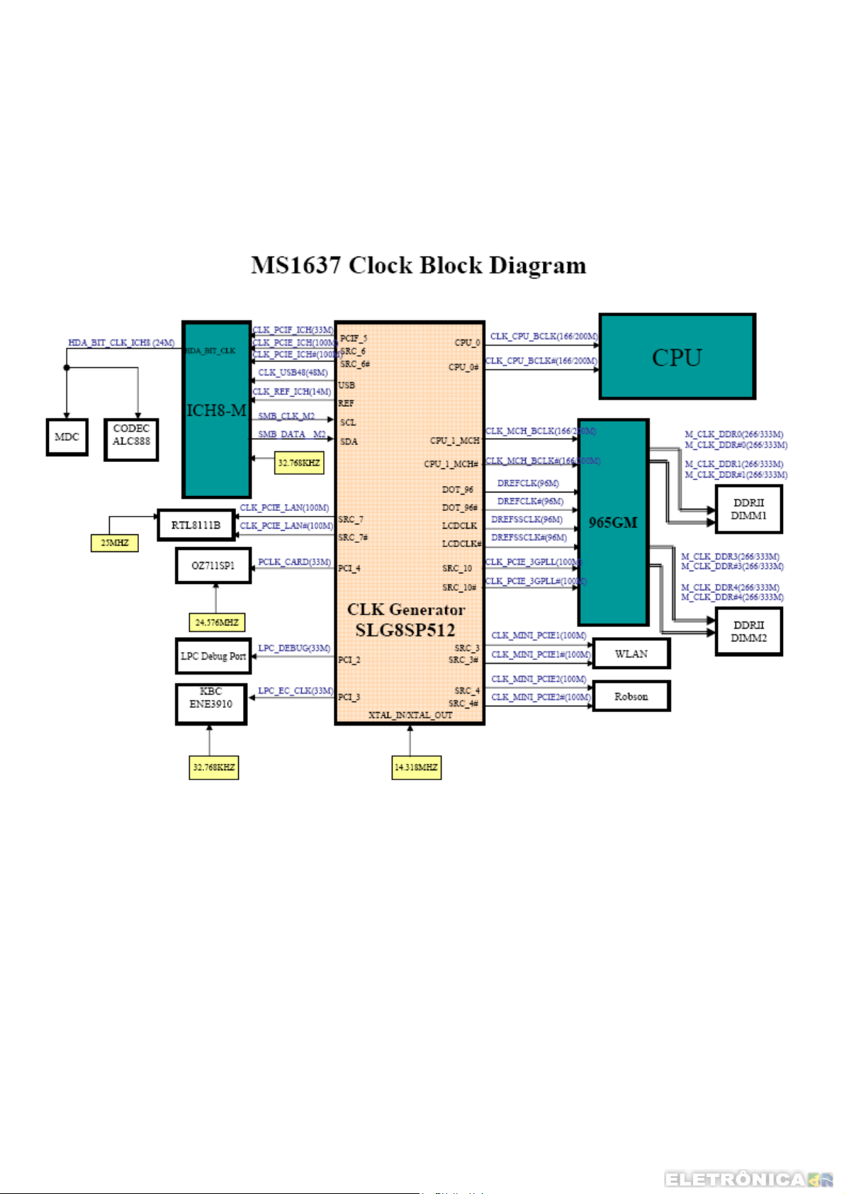
4、Clock Map & Repair Flow Chart
4.1、CLOCK MAP
Santa Rosa platform uses the CK505 single-chip clock solution. Figur e 1 and Figure 2 show the implementation of the clocks for a
typical platform, with an internal graphics solution
18
Page 20
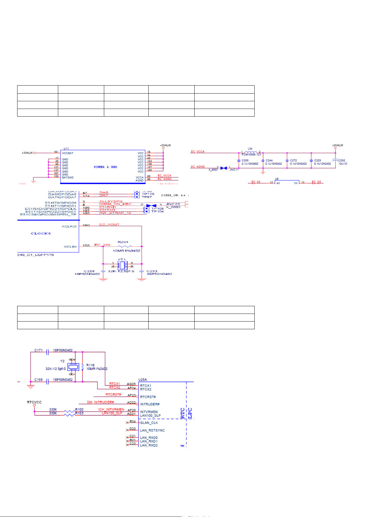
4.2 Repair Flow
If we find all power of system is ready, we must follow below steps for checking clocks whether is correct or not.
1. Check power (+3VALW) & clock of EC whether is active or not.
Item Subject Net name Level Measure Point
1 Power +3VALW +3.3V U11,PIN16
2 Clock EC_XIN 32.768KHZ U11,PIN158
3 Clock EC_XOUT 32.768KHZ U11,PIN160
2. Check RTC clock whether is active or not.
Item Subject Net name Level Measure Point
1 Clock RTCX1 32.768KHZ Y2,PIN4
2 Clock RTCX2 32.768KHZ Y2,PIN1
19
Page 21
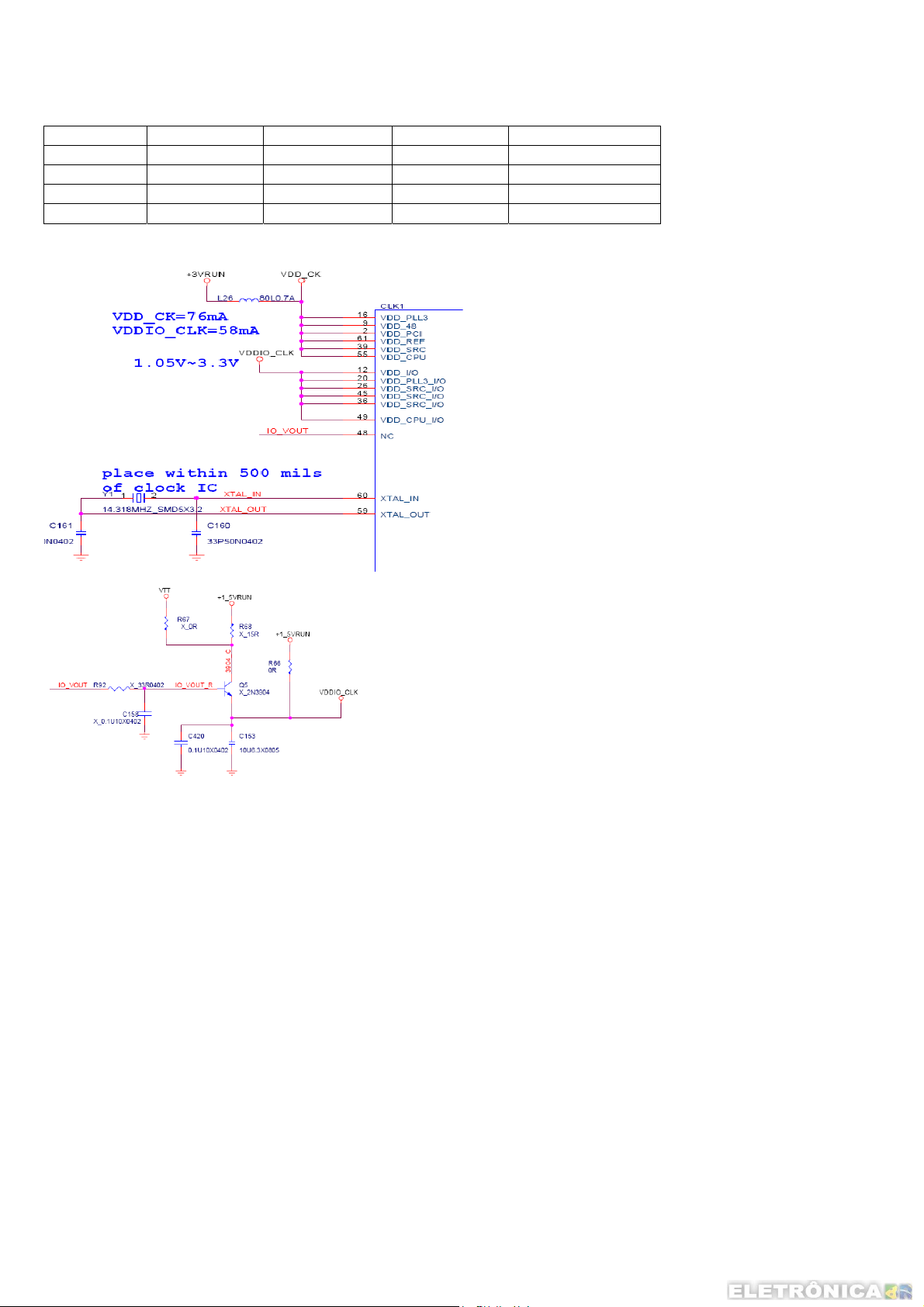
3. Check power (+3VMCLK&VDDIO_CLK) & clock of CLK Gen whether is active or not.
Item Subject Net name Level Measure Point
1 Power VDD_CK +3.3V L26
2 Power VDDIO_CLK +1.5V R66
3 Clock XTAL_IN 14.318MHZ Y1,PIN2
4 Clock XTAL_OUT 14.318MHZ Y1,PIN1
CLK Gen(CLK1) Schematic
20
Page 22
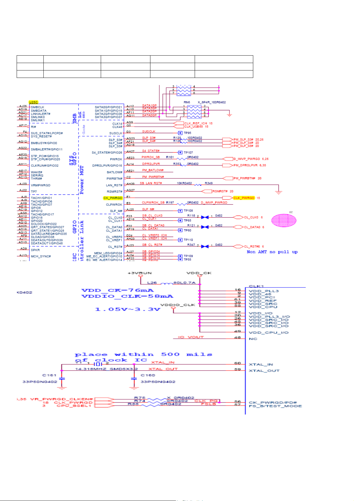
4. Check CLK_PWRGD whether is active or not.
Item Subject Net name Level Measure Point
1 Control Signal CLK_PWRGD V U28 _PIN F1
2 Control Signal CLKPG V CLK1 pin56,R74
21
Page 23
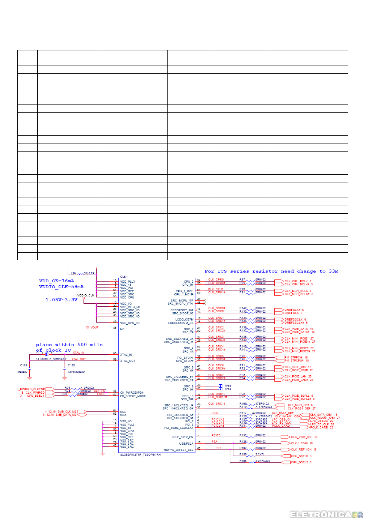
Check clocks of all frequency whether are active or not.
Item Subject Net name Level Measure Point Notice
1 PCI Clocks LPC_DEBUG 33.3MHZ R127
2 PCI Clocks PCLK_CARD 33.3MHZ R131
3 PCI Clocks LPC_EC_CLK 33.3MHZ R130
4 PCI Clocks PCLK_ICH 33.3MHZ R132
5 14MHZ Clocks XTAL_IN 14.318MHZ Y1
6 14MHZ Clocks XTAL_OUT 14.318MHZ Y1
7 14MHZ Clocks CLK_REF_ICH 14.318MHZ R107
8 48MHZ Clocks CLK_USB48 48MHZ R128
9 Host clocks CLK_CPU_BCLK 667/800MHZ CLK1, PIN54 CPU_BSEL(2,1,0)=0,0,1
10 Host clocks CLK_CPU_BCLK# 667/800MHZ CLK1, PIN53 CPU_BSEL(2,1,0)=0,0,1
11 Host clocks CLK_MCH_BCLK 667/800MHZ CLK1, PIN51 CPU_BSEL(2,1,0)=0,0,1
12 Host clocks CLK_MCH_BCLK# 667/800MHZ CLK1, PIN50 CPU_BSEL(2,1,0)=0,0,1
13 SRC clocks CLK_PCIE_3GPLL# 100MHZ CLK1, PIN35
14 SRC clocks CLK_PCIE_3GPLL 100MHZ CLK1, PIN34
15 SRC clocks CLK_PCIE_ICH 100MHZ CLK1, PIN41
16 SRC clocks CLK_PCIE_ICH# 100MHZ CLK1, PIN40
17 SRC clocks CLK_MINI_PCIE2 100MHZ CLK1, PIN27
18 SRC clocks CLK_MINI_PCIE2# 100MHZ CLK1, PIN28
19 SRC clocks CLK_MINI_PCIE1 100MHZ CLK1, PIN24
20 SRC clocks CLK_MINI_PCIE1# 100MHZ CLK1, PIN25
21 SRC clocks CLK_PCIE_SATA 100MHZ CLK1, PIN21
22 SRC clocks CLK_PCIE_SATA # 100MHZ CLK1, PIN22
23 SRC clocks DREFSSCLK 100MHZ CLK1, PIN17
24 SRC clocks DREFSSCLK# 100MHZ CLK1, PIN18
25 96MHZ Clocks DREFCLK 96MHZ CLK1, PIN13
26 96MHZ Clocks DREFCLK# 96MHZ CLK1, PIN14
22
Page 24
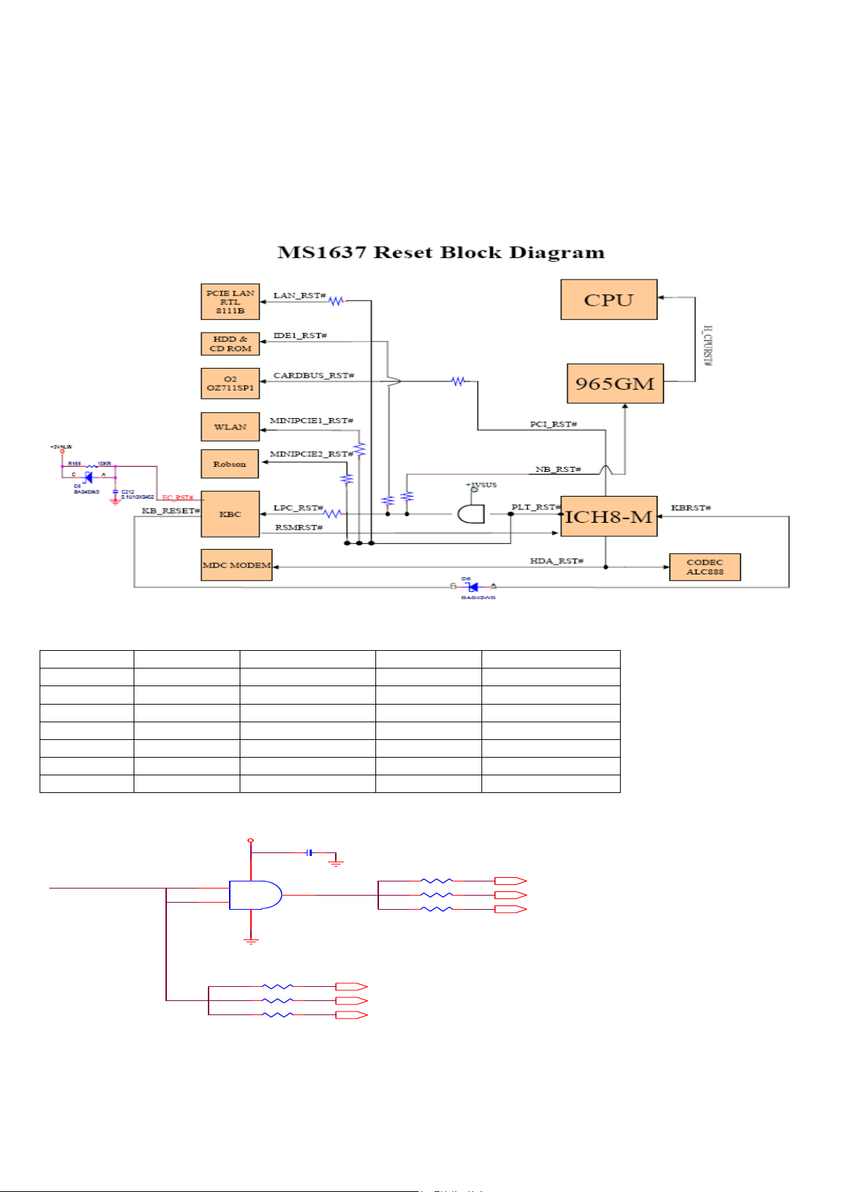
5、System Reset Map & Repair Flow Chart
If we find all power good signals of system is ready ,we must follow below steps for checking reset signals(RST#)
whether is correct or not.
1. Check PLT_RST# and RST# of other devices from SB whether is active or not.
Item Subject Net name Level Measure Point
1 RST# PLT_RST# V U6,PIN1
2 RST# LPC_RST# V R85
3 RST# MINIPCIE1_RST# V R86
4 RST# MINIPCIE2_RST# V R78
5 RST# IDE1_RST# V R76
6 RST# NB_RST# V R77
7 RST# LAN_RST# V R99
+3VSUS
C163 0.1U10X0402
PLT_RST#1
4
U6
NC7S08_SC70_5
3 5
R99 33R0402
R86 33R0402
R78 33R0402
R76 33R0402
R77 33R0402
R85 33R0402
LAN_RST# 25
MINIPCIE1_RST# 27
MINIPCIE2_RST# 27
IDE1_RST# 21
NB_RST# 6
LPC_RST# 20
PLT_RST#
VIH: MIN=2V
VIL:
MAX=0.8V
2
1
23
Page 25
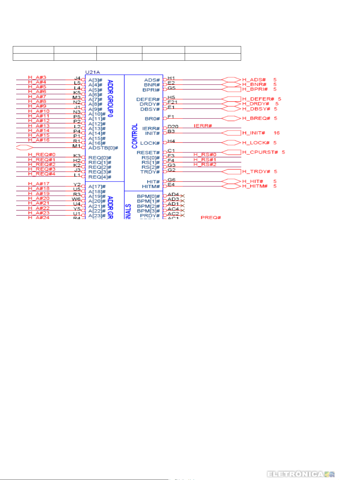
2. Check H_C P URST# for CPU whether is active or not.
Item Subject Net name Level Measure Point
1 RST# H_CPURST# V As below via
24
Page 26
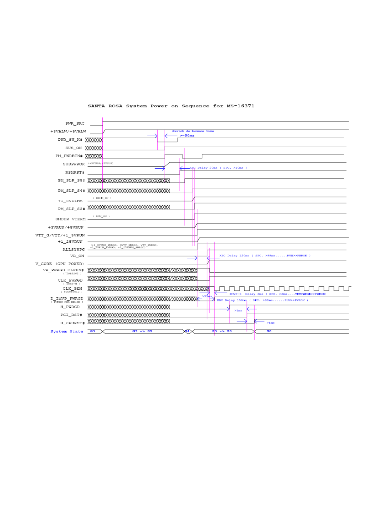
6、Power On Sequence
6.1 S5Æ S0
25
Page 27
7、AMI BIOS Check Point list
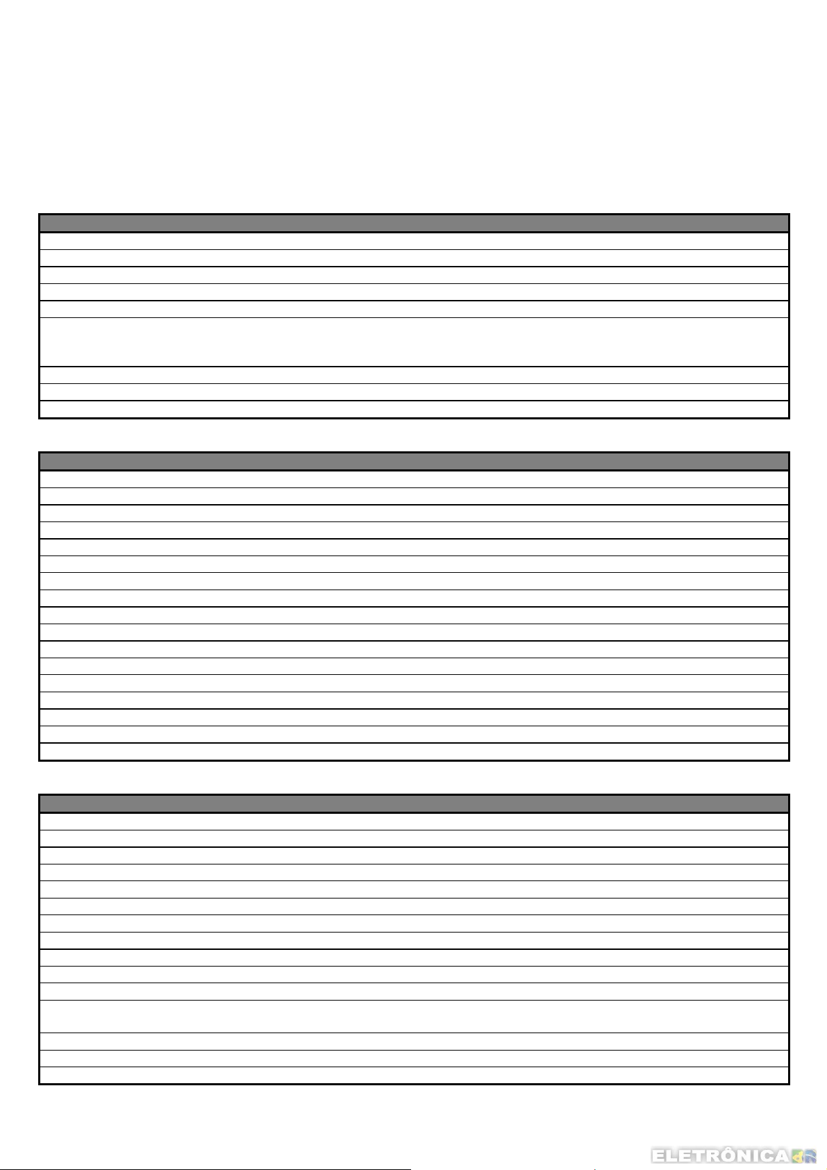
Following is the checkpoint list in AMIBIOS in order of execution.
1.Uncompressed INIT code checkpoints
Checkpoint Description
D0 NMI is Disabled. CPU ID saved. Init code Checksum verification starting.
D1 To do DMA init, Keyboard controller BAT test, start memory refresh and going to 4GB flat mode.
D3 To start Memory sizing.
D4 To comeback to real mode. Execute OEM patch. Set stack.
D5 E000 ROM enabled. Init code is copied to segment 0 and control to be transferred to segment 0.
D6 Control is in segment 0. To check <CTRL><HOME> key and verify main BIOS checksum. If either
<CTRL><HOME> is pressed or main BIOS checksum is bad, go to check point E0 else go to check
point D7.
D7 To pass control to Interface Module.
D8 Main BIOS runtime code is to be decompressed.
D9 Control to be passed to main BIOS in shadow RAM.
2. Boot Block Recovery Code Check Points
Checkpoint Meaning
E0 On Board Floppy Controller (if any) is initialized. To start base 512K memory test.
E1 To initialize interrupt vector table.
E2 To initialize DMA and interrupt controllers.
E6 To enable floppy and timer IRQ, enable internal cache.
ED Initialize floppy drive.
EE Start looking for a diskette in drive A: and read 1st sector of the diskette.
EF Floppy read error.
F0 S tart searching AMIBOOT.ROM file in root directory.
F1 AMIBOOT.ROM file not present in root directory.
F2 Start reading FAT table and analyze FAT to find the clusters occupied by AMIBOOT.ROM file.
F3 S tart reading AMIBOOT.ROM file cluster by cluster.
F4 AMIBOOT.ROM file not of proper size.
F5 Disable internal cache.
FB Detect Flash type present.
FC Erase Flash.
FD Program Flash.
FF Flash program successful. BIOS is going to restart.
3.Runtime code is uncompressed in F000 shadow ram
Checkpoint Meaning
03 NMI is Disabled. To check soft reset/power-on.
05 BIOS stack set. Going to disable Cache if any.
06 POST code to be uncompressed.
07 CPU init and CPU data area init to be done.
08 CMOS checksum calculation to be done next.
0B Any initialization before keyboard BAT to be done next.
0C KB controller I/B free. To issue the BAT command to keyboard controller.
0E Any initialization after KB controller BAT to be done ne x t.
0F Keyboard command byte to be written.
10 Going to issue Pin-23,24 blocking/unblocking command.
11 Going to check pressing of <INS> , <END> key during power-o n.
12
13 Video display is disabled and port-B is initialized. Chipset init about to begin.
14 8254 timer test about to start.
19 About to start memory refresh test.
To init CMOS if nit CMOS in every boot” is set or <END> key is pressed. Going to disable DMA and
Interrupt controllers.
26
Page 28
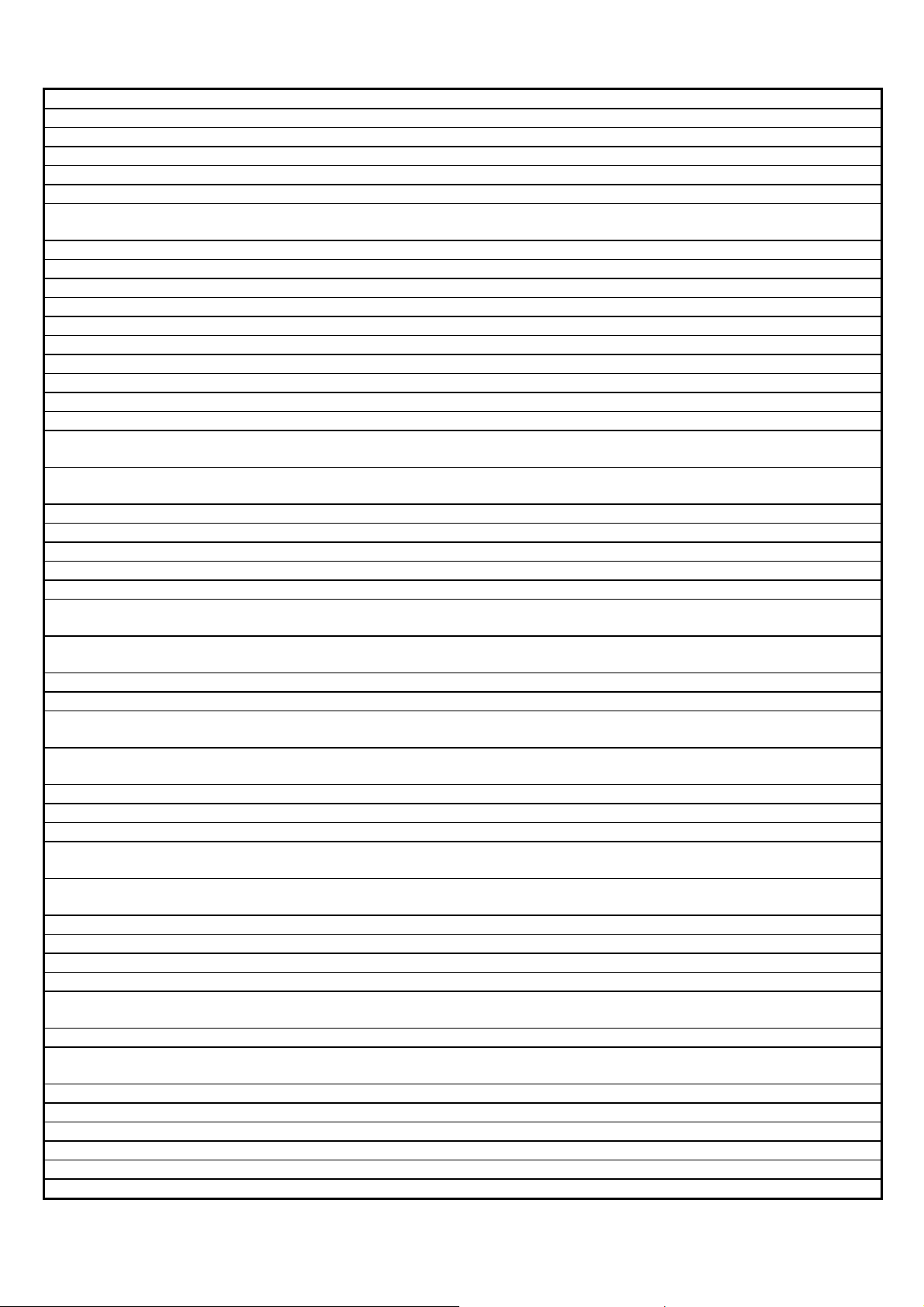
1A Memory Refresh line is toggling. Going to check 15us ON/OFF time.
23 To read 8042 input port and disable Megakey Green PC feature. Make BIOS code segment writeable.
24 To do any setup before Int vector init.
25 Interrupt vector initialization about to begin. To clear password if nece ssary.
27 Any initialization before setting video mode to be done.
28 Going for monochrome mode and color mode setting.
2A
Different BUSes init (system, static, output devices) to start if present. (Please see Appendix for details
of different BUSes).
2B To give control for any setup required before optional video ROM check.
2C To look for optional video ROM and give control.
2D To give control to do any processing after video ROM returns control.
2E If EGA/VGA not found then do display memory R/W test.
2F EGA/VGA not found. Display memory R/W test about to begin.
30 Display memory R/W test passed. About to look for the retrace checking.
31 Display memory R/W test or retrace checking failed. To do alternate Display memory R/W test.
32 Alternate Display memory R/W test passed. To look for the alternate display retrace checking.
34 Video display checking over. Display mode to be set next.
37 Display mode set. Going to display the power on message.
38
39
Different BUSes init (input, IPL, general devices) to start if present. (Please see Appendix for details of
different BUSes).
Display different BUSes initialization error messages. (Please see Appendix for details of different
BUSes).
3A New cursor position read and saved. To display the Hit <DEL> message.
40 To prepare the descriptor tables.
42 To enter in virtual mode for memory test.
43 To enable interrupts for diagnostics mode.
44 To initialize data to check memory wrap around at 0:0.
45
46
Data initialized. Going to check for memory wrap around at 0:0 and finding the tot al system memory
size.
Memory wrap around test done. Memory size calculation over. About to go for writing patterns to test
memory.
47 Pattern to be tested written in extended memory. Going to write patterns in base 640k memory.
48 Patterns written in base memory. Going to find out amount of memory below 1M memory.
49
4B
Amount of memory below 1M found and verified. Going to find out amount of memory above 1M
memory.
Amount of memory above 1M found and verified. Check for soft reset and going to clear memory below
1M for soft reset. (If power on, go to check point# 4Eh).
4C Memory below 1M cle ared.(SOFT RESET) Going to clear memory above 1M.
4D Memory above 1M cleare d.(SOFT RESET) Going to save the memory size. (Goto check point# 52h).
4E Memory test started. (NOT SOFT RESET) About to display the first 64k memory size.
4F
50
Memory size display started. This will be updated during memory test. Going for sequential and random
memory test.
Memory testing/initialization below 1M complete. Going to adjust displayed memory size for relocation/
shadow.
51 Memory size display adjusted due to relocation/ shadow. Memory test above 1M to follow.
52 Memory testing/initialization above 1M complete. Going to save memory size information.
53 Memory size information is saved. CPU registers are saved. Going to enter in real mode.
54 Shutdown successful, CPU in real mode. Going to disable gate A20 line and disable parity/NMI.
57
A20 address line, parity/NMI disable successful. Going to adjust memory size depe nding on
relocation/shadow.
58 Memory size adjusted for relocation/shadow. Going to clear Hit <DEL> message.
59
Hit <DEL> message cleared. <WAIT...> message displayed. About to start DMA and interrupt controller
test.
60 DMA page register test p assed. To do DMA#1 base register test.
62 DMA#1 base register test passed. To do DMA#2 base register test.
65 DMA#2 base register test passed. To program DMA unit 1 and 2.
66 DMA unit 1 and 2 programming over. To initialize 8259 interrupt controller.
7F Extended NMI sources enabling is in progress.
80 Keyboard test started. clearing output buffer, checking for stuck key, to issue keyboard reset command.
27
Page 29
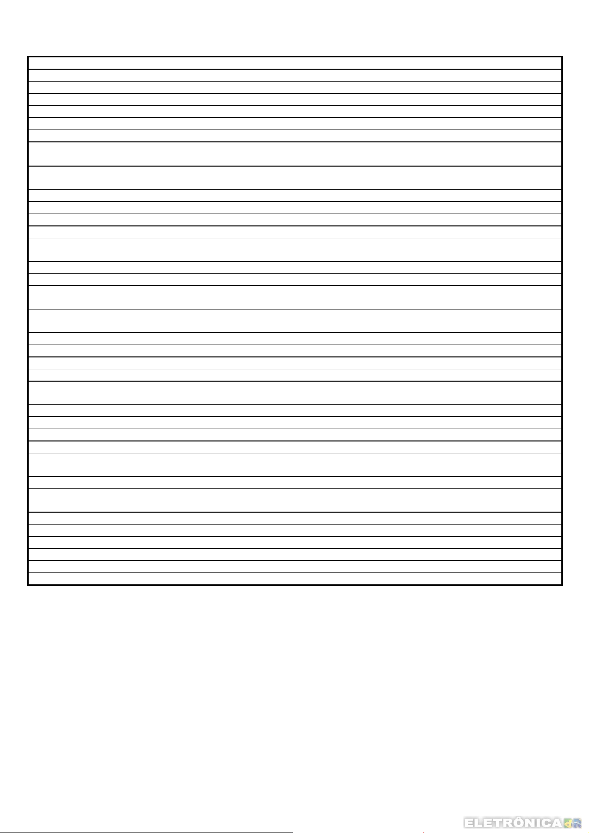
81 Keyboard reset error/stuck key found. To issue keyboard co ntroller interface test command.
82 Keyboard controller interface test over. To write command byte and init circular buffer.
83 Command byte written, Global data init done. To check for lock-key.
84 Lock-key checking over. To check for memory size mismatch with CMOS.
85 Memory size check done. To display sof t error and check for password or bypass setup.
86 Password checked. About to do programming before setup.
87 Programming before setup complete. To uncompress SETUP code and execute CMOS setup.
88 Returned from CMOS setup program and screen is cleared. About to do programming after setup.
89 Programming after setup complete. Going to display power on screen message.
8B
First screen message displayed. <WAIT...> message displayed. PS/2 Mouse check and extended BIOS
data area allocation to be done.
8C Setup options programming after CMOS setup about to start.
8D Going for hard disk controll er reset.
8F Hard disk controller reset done. Floppy setup to be done next.
91 Floppy setup complete. Hard disk setup to be done next.
95
Init of different BUSes optional ROMs from C800 to start. (Please see Appendix-I for details of dif f erent
BUSes).
96 Going to do any init before C800 optional ROM control.
97 Any init before C800 optional ROM control is over. Optional ROM check and control will be done next.
98
99
Optional ROM control is done. About to give control to do any required processing after optional ROM
returns control and enable external cache.
Any initialization required after optional ROM test over. Going to setup timer data area and printer base
address.
9A Return after setting timer and printer base address. Going to set the RS-232 base address.
9B Returned after RS-232 base address. Going to do any initialization before Coprocessor test.
9C Required initialization before Coprocessor is over. Going to initialize the Coprocessor next.
9D Coprocessor initialized. Going to do any initialization after Coprocessor test.
9E
Initialization after Coprocessor test is complete. Going to check extd keyboard, keyboard ID and
num-lock. Keyboard ID command to be
A2 Going to display any soft errors.
A3 Soft error display complete. Going to set keyboard typematic rate.
A4 Keyboard typematic rate set. To program memory wait states.
A5 Going to enable parity/NMI.
A7
NMI and parity enabled. Going to do any initialization required before giving control to option al ROM at
E000.
A8 Initialization before E000 ROM control over. E000 ROM to get control next.
A9
Returned from E000 ROM control. Going to do any initialization required after E000 optional ROM
control.
AA Initialization after E000 optional ROM control is over. Going to display the system configuration.
AB To build MP table if needed.
AC To uncompress DMI data and execute DMI POST init.
B0 System configuration is displayed.
B1 Going to copy any code to specific area.
00 Copying of code to specific area done. Going to give control to INT-19 boot loader.
28
 Loading...