

Page 1
G41M Series
MS-7563 (V1.X) Mainboard
G52-75631X3
i
Page 2

Copyright Notice
The material in this document is the intellectual property of MICRO-STAR
INTERNATIONAL. We take every care in the preparation of this document, but no
guarantee is given as to the correctness of its contents. Our products are under
continual improvement and we reserve the right to make changes without notice.
Trademarks
All trademarks are the properties of their respective owners.
NVIDIA, the NVIDIA logo, DualNet, and nForce are registered trademarks or trade-
marks of NVIDIA Corporation in the United States and/or other countries.
AMD, Athlon™ , Athlon™ XP, Thoroughbred™, and Duron™ are registered trademarks of AMD Corporation.
Intel® and Pentium® are registered trademarks of Intel Corporation.
PS/2 and OS®/2 are registered trademarks of International Business Machines
Corporation.
Windows® 2000/NT/XP/Vista are registered trademarks of Microsoft Corporation.
Netware® is a registered trademark of Novell, Inc.
Award® is a registered trademark of Phoenix Technologies Ltd.
AMI® is a registered trademark of American Megatrends Inc.
Revision History
Revision Revision History Date
V1.0 First release for Asia November 2008
Technical Support
If a problem arises with your system and no solution can be obtained from the user’ s
manual, please contact your place of purchase or local distributor. Alternatively,
please try the following help resources for further guidance.
Visit the MSI website for FAQ, technical guide, BIOS updates, driver updates,
and other information: http://global.msi.com.tw/index.php?
func=service
Contact our technical staff at: http://ocss.msi.com.tw
ii
Page 3
Safety Instructions
1. Always read the safety instructions carefully.
2. Keep this User’s Manual for future reference.
3. Keep this equipment away from humidity.
4. Lay this equipment on a reliable flat surface before setting it up.
5. The openings on the enclosure are for air convection hence protects the equipment from overheating. DO NOT COVER THE OPENINGS.
6. Make sure the voltage of the power source and adjust properly 110/220V before connecting the equipment to the power inlet.
7. Place the power cord such a way that people can not step on it. Do not place
anything over the power cord.
8. Always Unplug the Power Cord before inserting any add-on card or module.
9. All cautions and warnings on the equipment should be noted.
10. Never pour any liquid into the opening that could damage or cause electrical
shock.
11. If any of the following situations arises, get the equipment checked by service
personnel:
† The power cord or plug is damaged.
† Liquid has penetrated into the equipment.
† The equipment has been exposed to moisture.
† The equipment does not work well or you can not get it work according to
User’s Manual.
† The equipment has dropped and damaged.
† The equipment has obvious sign of breakage.
12. DO NOT LEAVE THIS EQUIPMENT IN AN ENVIRONMENT UNCONDITIONED, STORAGE TEMPERATURE ABOVE 600 C (1400F), IT MAY DAMAGE THE EQUIPMENT.
CAUTION: Danger of explosion if battery is incorrectly replaced.
Replace only with the same or equivalent type recommended by the
manufacturer.
iii
Page 4
FCC-B Radio Frequency Interference Statement
This equipment has been
tested and found to comply
with the limits for a Class B
digital device, pursuant to Part
15 of the FCC Rules. These limits are designed to provide reasonable protection
against harmful interference in a residential installation. This equipment generates,
uses and can radiate radio frequency energy and, if not installed and used in accordance with the instructions, may cause harmful interference to radio communications.
However, there is no guarantee that interference will not occur in a particular
installation. If this equipment does cause harmful interference to radio or television
reception, which can be determined by turning the equipment off and on, the user is
encouraged to try to correct the interference by one or more of the measures listed
below.
† Reorient or relocate the receiving antenna.
† Increase the separation between the equipment and receiver.
† Connect the equipment into an outlet on a circuit different from that to
which the receiver is connected.
† Consult the dealer or an experienced radio/television technician for help.
Notice 1
The changes or modifications not expressly approved by the party responsible for
compliance could void the user’s authority to operate the equipment.
Notice 2
Shielded interface cables and A.C. power cord, if any, must be used in order to
comply with the emission limits.
VOIR LA NOTICE D’ INSTALLATION AVANT DE RACCORDER AU RESEAU.
Micro-Star International
MS-7563
This device complies with Part 15 of the FCC Rules. Operation is subject to the
following two conditions:
(1) this device may not cause harmful interference, and
(2) this device must accept any interference received, including interference that
may cause undesired operation.
iv
Page 5
WEEE (Waste Electrical and Electronic Equipment) Statement
v
Page 6
vi
Page 7
vii
Page 8

CONTENTS
Copyright Notice.......................................................................................................ii
Trademarks..............................................................................................................ii
Revision History.......................................................................................................ii
Technical Support....................................................................................................ii
Safety Instructions...................................................................................................iii
FCC-B Radio Frequency Interference Statement...................................................iv
WEEE (Waste Electrical and Electronic Equipment) Statement............................v
English..............................................................................................En-1
Mainboard Specifications.........................................................................................En-2
Quick Components Guide........................................................................................En-4
CPU (Central Processing Unit)................................................................................En-5
Memory.....................................................................................................................En-9
Power Supply...........................................................................................................En-11
Back Panel...............................................................................................................En-12
Connectors...............................................................................................................En-14
Jumper......................................................................................................................En-22
Slots..........................................................................................................................En-23
BIOS Setup..............................................................................................................En-25
Software Information................................................................................................En-32
......................................................................................................................
한국어
메인보드 사양 ..........................................................................................................Kr-2
빠른 부품 설명서.....................................................................................................Kr-4
CPU (중앙 처리 장치).............................................................................................Kr-5
메모리.......................................................................................................................Kr-9
전원 공급장치 ..........................................................................................................Kr-11
후면 패널..................................................................................................................Kr-12
커넥터.......................................................................................................................Kr-14
점퍼...........................................................................................................................Kr-22
슬롯...........................................................................................................................Kr-23
BIOS 설정................................................................................................................Kr-25
소프트웨어 정보.......................................................................................................Kr-32
Kr-1
viii
Page 9

日本語..................................................................................................................... Jp-1
マザーボードの仕様.................................................................................................Jp-2
クイックコンポーネントガイド..............................................................................Jp-4
CPU に関する注意事項 ...........................................................................................Jp-5
メモリ.......................................................................................................................Jp-9
電源 ..........................................................................................................................Jp-11
バックパネル............................................................................................................Jp-12
コネクター...............................................................................................................Jp-14
ジャンパ...................................................................................................................Jp-22
スロット...................................................................................................................Jp-23
BIOS の設定.............................................................................................................Jp-25
ソフトウェアの情報.................................................................................................Jp-32
繁體中文................................................................................... Tc-1
主機板規格.............................................................................................................Tc-2
快速安裝指南..........................................................................................................Tc-4
中央處理器..............................................................................................................Tc-5
記憶體......................................................................................................................Tc-9
電源供應器..............................................................................................................Tc-11
背板..........................................................................................................................Tc-12
連接器......................................................................................................................Tc-14
跳線..........................................................................................................................Tc-22
插槽..........................................................................................................................Tc-23
BIOS 設定 ...............................................................................................................Tc-25
軟體訊息..................................................................................................................Tc-32
简体中文.............................................................................................Sc-1
主板规格....................................................................................................................Sc-2
组件指南....................................................................................................................Sc-4
中央处理器: CPU.......................................................................................................Sc-5
内存...........................................................................................................................Sc-9
电源适配器.................................................................................................................Sc-11
后置面板....................................................................................................................Sc-12
ix
Page 10

接口...........................................................................................................................Sc-14
跳线...........................................................................................................................Sc-22
插槽...........................................................................................................................Sc-23
BIOS 设置.................................................................................................................Sc-25
软件信息....................................................................................................................Sc-32
x
Page 11

G41M
Series
User’s Guide
Engli sh
English
En-1
Page 12

MS-7563 Mainboard
Mainboard Specifications
Processor Support
- Intel® Core 2 Quad/ Core 2 Duo/ / Yorkfield/ Wolfdale processors in
LGA775 package
- Supports 4 pin CPU Fan Pin-Header with Fan Speed Control
(For the latest information about CPU, please visit
http://global.msi.com.tw/index.php?func=cpuform2)
Supported FSB
- 1333/ 1066/ 800 MHz
Chipset
- North Bridge: Intel® G41 chipset
- South Bridge: Intel® ICH7 chipset
Memory Support
- DDR2 667/800 SDRAM (8GB Max)
- 2 DDR2 DIMMs (240pin / 1.8V)
(For more information on compatible components, please visit
http://global.msi.com.tw/index.php?func=testreport)
LAN
- Supports 10/100/1000 Fast Ethernet by Realtek 8111DL
Audio
- Chip integrated by Realtek® ALC888
- Flexible 8-channel audio with jack sensing
- Supports Vista premium compliance
IDE
- 1 IDE port by ICH7
- Supports Ultra DMA 66/100 mode
- Supports PIO, Bus Master operation mode
SATA
- 4 SATA ports by ICH7
- Supports storage and data transfers at up to 3 Gb/s
Floppy
- 1 floppy port
- Supports 1 FDD with 360KB, 720KB, 1.2MB, 1.44MB and 2.88MB
Connectors
Back panel
- 1 PS/2 mouse port
- 1 PS/2 keyboard port
- 1 VGA port
En-2
Page 13
- 1 DVI-D port
- 1 DisplayPort jack
- 4 USB 2.0 Ports
- 1 RJ-45 LAN jack
- 1 1394 port (optional)
- 6 flexible audio jacks
On-Board Pinheaders/ Connectors
- 2 USB 2.0 pinheaders
- 1 CD-in pinheader
- 1 SPDIF-Out pinheader
- 1 IEEE 1394 pinheader (optional)
- 1 Front Panel Audio pinheader
- 1 Serial port pinheader
- 1 TPM (optional)
- 1 Chassis Intrusion Switch pinheader
- 1 Parallel Port pinheader
Slots
- 1 PCI Express x16 slot
- 1 PCI Express x 1 slot
- 2 PCI slots
- Support 3.3V/ 5V PCI bus Interface
Form Factor
- Micro-ATX (24.4cm X 22.8cm)
Mounting
- 6 mounting holes
Engli sh
En-3
Page 14
MS-7563 Mainboard
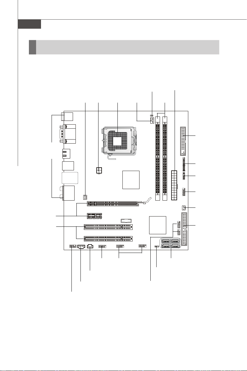
Quick Components Guide
Back Panel,
En-12
PCIE,
En-23
PCI,
En-23
SYSFAN1,
En-16
JAUD1,
En-19
JSPD1,
En-17
CD_IN1,
En-18
JPW1,
En-11
J1394_1,
En-17
CPU,
En-5
JUSB1/2,
En-20
CPUFAN1,
En-16
JFP1/2,
En-18
JCI1,
En-16
JBAT1,
En-22
ATX1,
En-11
DDR2,
En-9
FDD1,
En-14
JLPT1,
En-21
JTPM1,
En-19
JCOM1,
En-20
SYSFAN2,
En-16
IDE1,
En-14
SATA1~4,
En-15
En-4
Page 15
CPU (Central Processing Unit)
When you are installing the CPU, make sure to install the cooler to prevent
overheating. If you do not have the CPU cooler, consult your dealer before turning
on the computer.
For the latest information about CPU, please visit http://global.msi.com.tw/index.php?
func=cpuform2
Important
Overheating
Overheating will seriously damage the CPU and system. Always make sure
the cooling fan can work properly to protect the CPU from overheating. Make
sure that you apply an even layer of thermal paste (or thermal tape) between
the CPU and the heatsink to enhance heat dissipation.
Replaceing the CPU
While replacing the CPU, always turn off the ATX power supply or unplug the
power supply’s power cord from the grounded outlet first to ensure the safety
of CPU.
Overclocking
This mainboard is designed to support overclocking. However, please make
sure your components are able to tolerate such abnormal setting, while
doing overclocking. Any attempt to operate beyond product specifications is
not recommended. We do not guarantee the damages or risks caused
by inadequate operation or beyond product specifications.
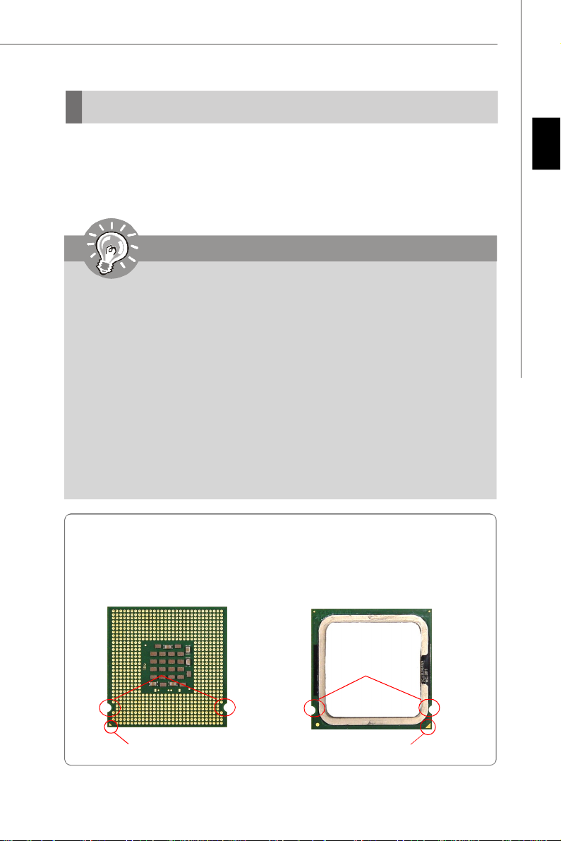
Introduction to LGA 775 CPU
The pin-pad side of LGA 775
CPU.
The surface of LGA 775 CPU.
Remember to apply some thermal paste on it for better heat
dispersion.
Engli sh
Alignment Key Alignment Key
Yellow triangle is the Pin 1 indicator
Yellow triangle is the Pin 1 indicator
En-5
Page 16
MS-7563 Mainboard
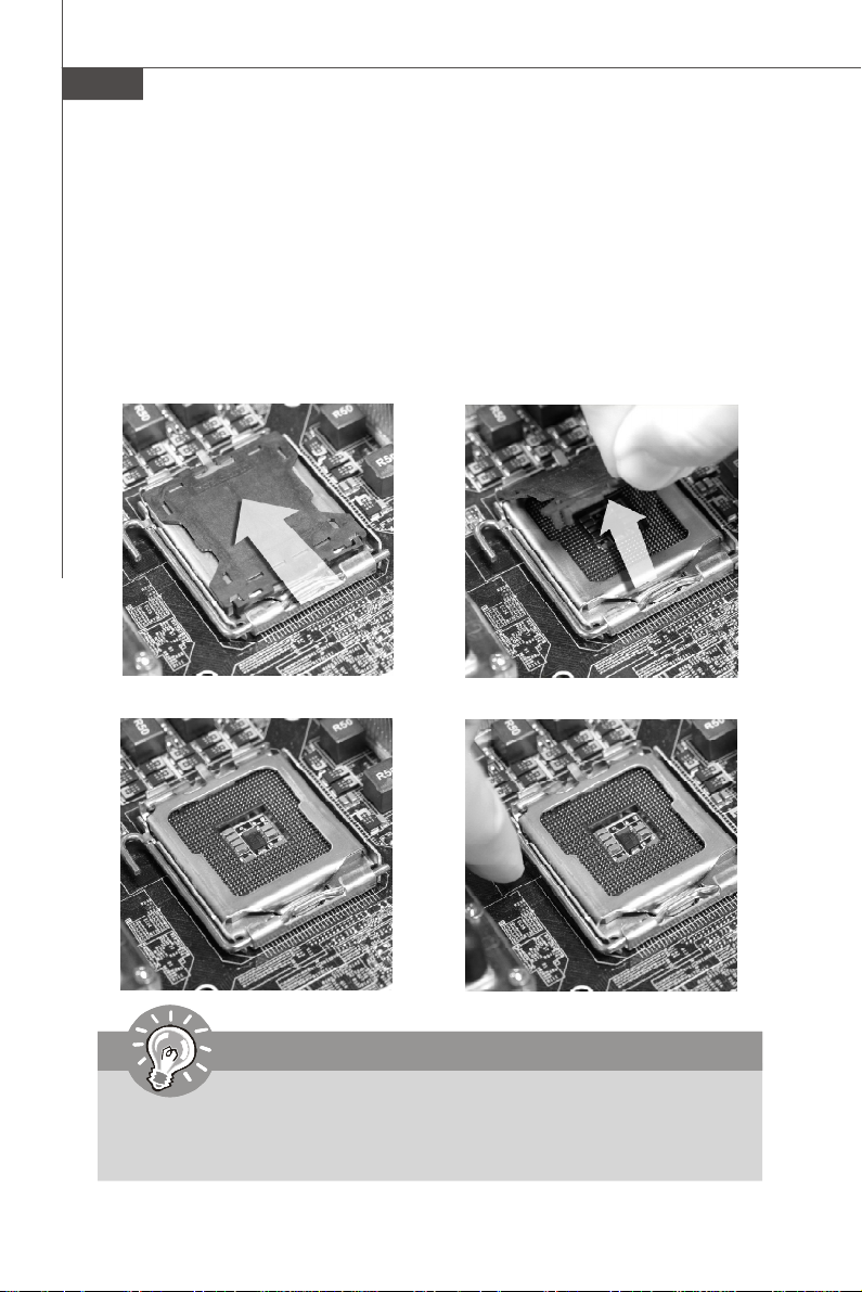
CPU & Cooler Installation
When you are installing the CPU, make sure the CPU has a cooler attached on
the top to prevent overheating. Meanwhile, do not forget to apply some thermal
paste on CPU before installing the heat sink/cooler fan for better heat dispersion.
Follow the steps below to install the CPU & cooler correctly. Wrong installation will
cause the damage of your CPU & mainboard.
1.The CPU socket has a plastic cap on
it to protect the contact from damage.
Before you install the CPU, always
cover it to protect the socket pin.
3.The pins of socket reveal.
2.Remove the cap from lever hinge
side (as the arrow shows).
4.Open the load lever.
Important
1.Confirm if your CPU cooler is firmly installed before turning on your system.
2. Do not touch the CPU socket pins to avoid damaging.
3. The availability of the CPU land side cover depends on your CPU packing.
En-6
Page 17
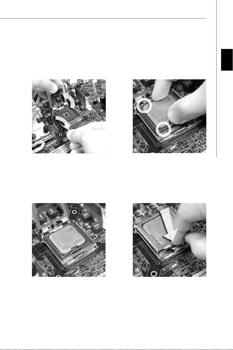
5.Lift the load lever up and open the
load plate.
6.After confirming the CPU direction
for correct mating, put down the
CPU in the socket housing frame.
Be sure to grasp on the edge of
the CPU base. Note that the alignment keys are matched.
alignment
key
Engli sh
7.Visually inspect if the CPU is
seated well into the socket. If not,
take out the CPU with pure vertical
motion and reinstall.
8.Cover the load plate onto the
package.
En-7
Page 18
MS-7563 Mainboard
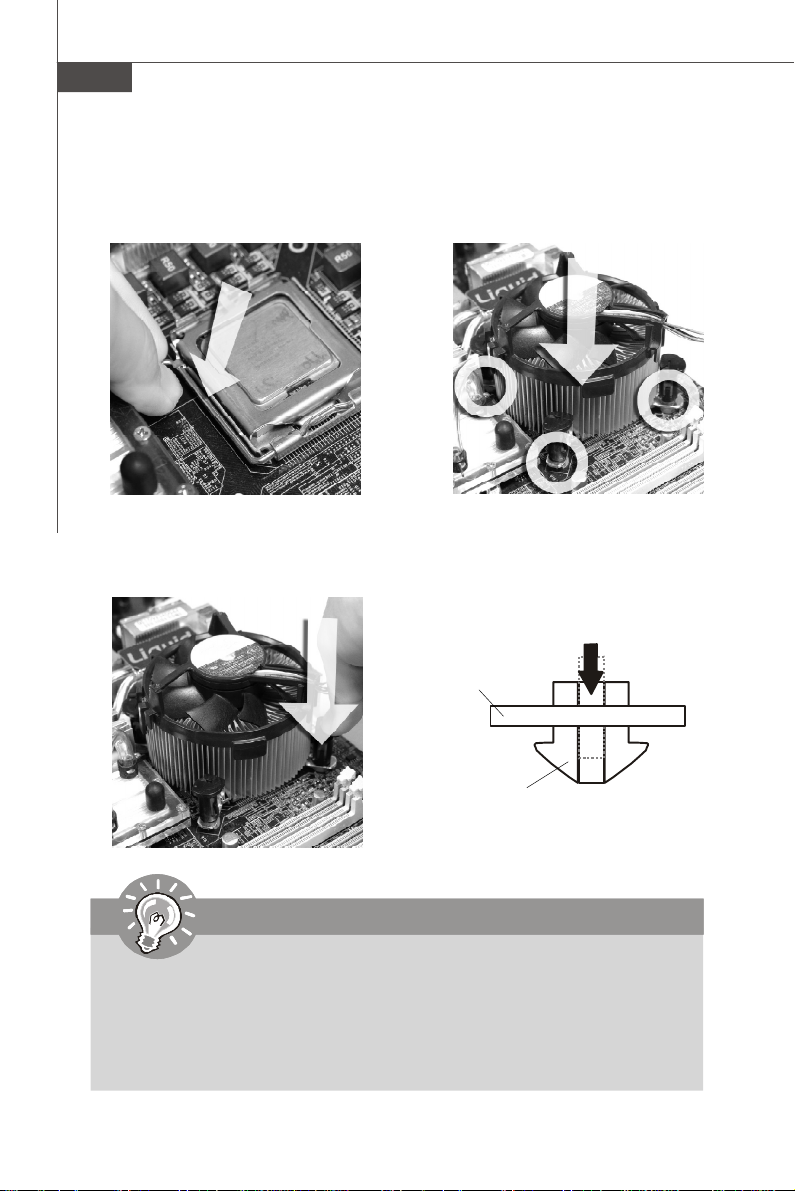
9.Press down the load lever lightly
onto the load plate, and then secure the lever with the hook under
retention tab.
11.Press the four hooks down to fasten
the cooler. Then rotate the locking
switch (refer to the correct direction
marked on it) to lock the hooks.
10. Align the holes on the mainboard
with the heatsink. Push down the
cooler until its four clips get
wedged into the holes of the
mainboard.
12.Turn over the mainboard to confirm that the clip-ends are correctly
inserted.
Mainboard
locking
switch
Hook
Important
1. Read the CPU status in BIOS.
2. Whenever CPU is not installed, always protect your CPU socket pin with the
plastic cap covered (shown in Figure 1) to avoid damaging.
3. Mainboard photos shown in this section are for demonstration of the CPU/
cooler installation only. The appearance of your mainboard may vary depending on the model you purchase.
En-8
Page 19
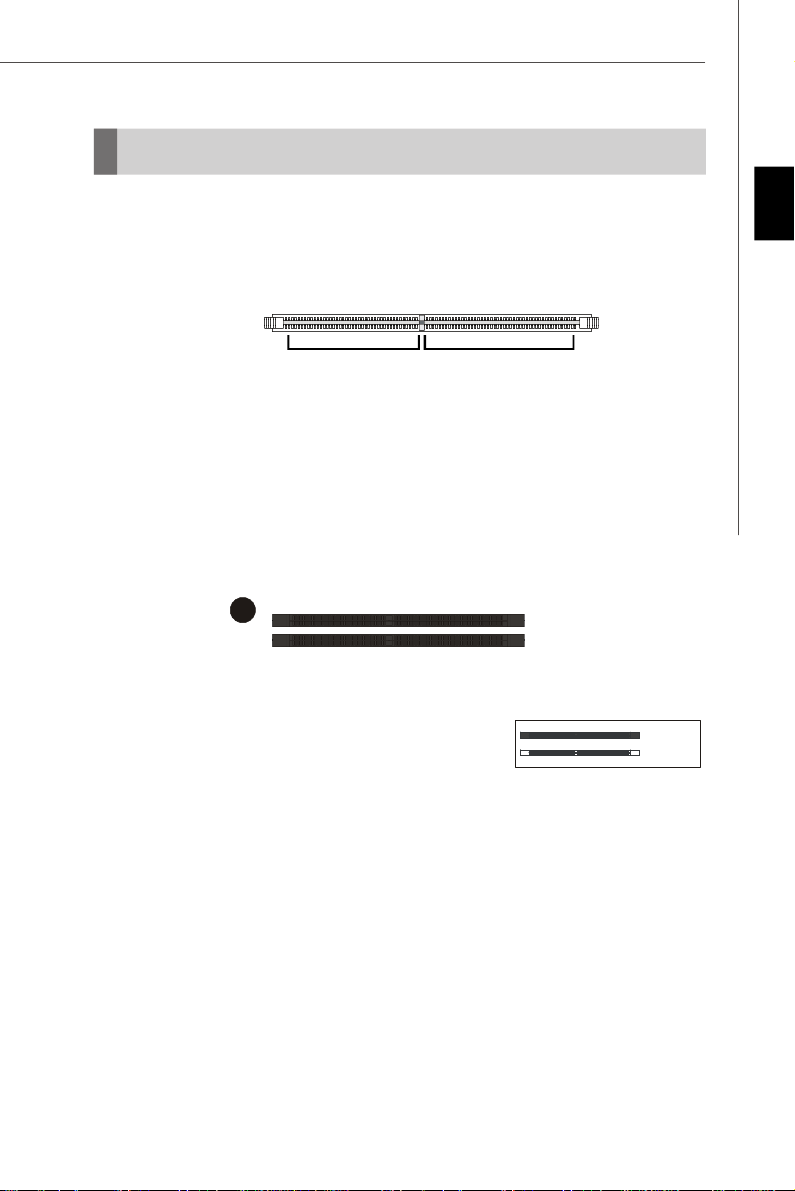
Memory
Installed
1
These DIMM slots are used for installing memory modules.
For more information on compatible components, please visit http://global.msi.com.
tw/index.php?func=testreport
DDR2
240-pin, 1.8V
64x2=128 pin56x2=112 pin
Dual-Channel Memory Population Rules
In Dual-Channel mode, the memory modules can transmit and receive data with two
data bus lines simultaneously. Enabling Dual-Channel mode can enhance the system
performance. Please refer to the following illustrations for population rules under
Dual-Channel mode.
DIMM1
DIMM2
Engli sh
Empty
En-9
Page 20
MS-7563 Mainboard
Installing Memory Modules
1. The memory module has only one notch on the center and will only fit in the right
orientation.
2. Insert the memory module vertically into the DIMM slot. Then push it in until the
golden finger on the memory module is deeply inserted in the DIMM slot. The plastic
clip at each side of the DIMM slot will automatically close when the memory module
is properly seated.
Important
You can barely see the golden finger if the memory module is properly inserted
in the DIMM slot.
3. Manually check if the memory module has been locked in place by the DIMM slot
clips at the sides.
Volt
Notch
Important
-DDR2 memory modules are not interchangeable with DDR and the DDR2
standard is not backwards compatible. You should always install DDR2
memory modules in the DDR2 DIMM slots.
-In Dual-Channel mode, make sure that you install memory modules of the
same type and density in different channel DIMM slots.
-To enable successful system boot-up, always insert the memory modules
into the DIMM1 first.
En-10
Page 21
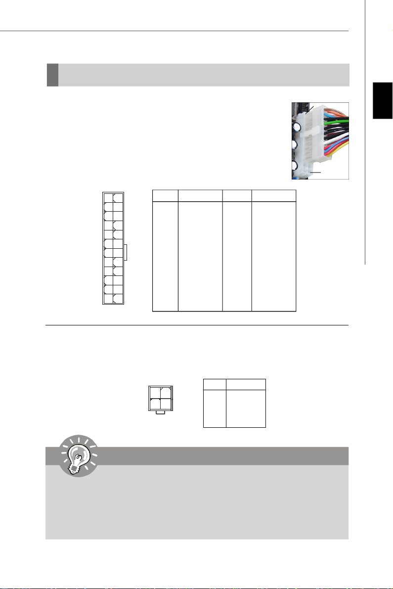
Power Supply
ATX 24-Pin Power Connector: ATX1
This connector allows you to connect an ATX 24-pin power supply.
To connect the ATX 24-pin power supply, make sure the plug of the
power supply is inserted in the proper orientation and the pins are
aligned. Then push down the power supply firmly into the connector.
You may use the 20-pin ATX power supply as you like. If you’d like
to use the 20-pin ATX power supply, please plug your power supply along with pin 1 & pin 13 (refer to the image at the right hand).
Pin Definition
PIN SIGNAL
13 +3.3V
14 -12V
15 GND
16 PS-ON#
17 GND
18 GND
19 GND
20 Res
21 +5V
22 +5V
23 +5V
24 GND
ATX1
12
1
24
13
PIN SIGNAL
1 +3.3V
2 +3.3V
3 GND
4 +5V
5 GND
6 +5V
7 GND
8 PWR OK
9 5VSB
10 +12V
11 +12V
12 +3.3V
ATX 12V Power Connector: JPW1
This 12V power connector is used to provide power to the CPU.
Pin Definition
PIN SIGNAL
1 GND
2 GND
3 12V
4 12V
JPW1
2
4
1
3
pin 13
pin 12
English
Important
1. Make sure that all the connectors are connected to proper ATX power supplies to ensure stable operation of the mainboard.
2. Power supply of 350 watts (and above) is highly recommended for system
stability.
3. ATX 12V power connection should be greater than 18A.
En-11
Page 22
MS-7563 Mainboard
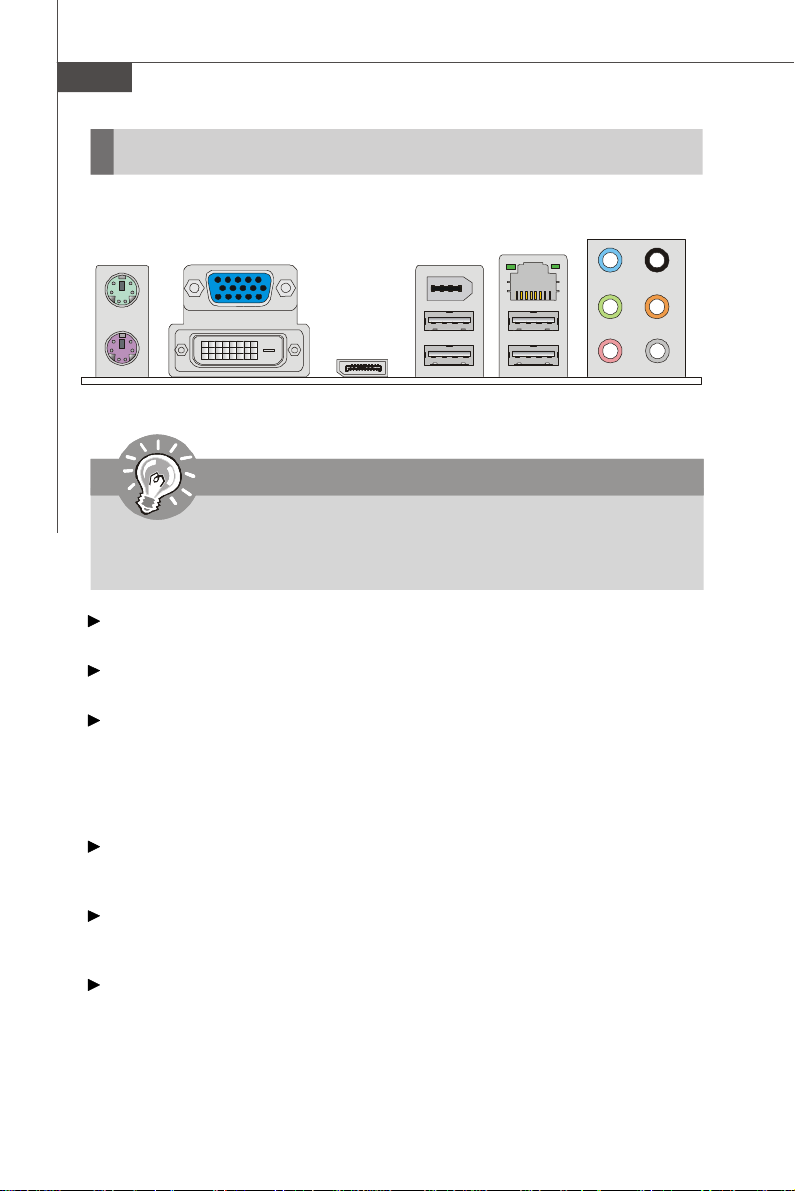
Back Panel
Mouse
Keyboard
VGA Port
DVI-D Port
DisplayPort
1394
Port
(optional)
USB Ports Mic
LAN
Line-In
Line-Out
RS-Out
CS-Out
SS-Out
Important
When there is any expansion card inserted in the PCIE x16 slot, the VGA,
DisplayPort and DVI-D port will not output any signal.
Mouse/Keyboard
The standard PS/2® mouse/keyboard DIN connector is for a PS/2® mouse/keyboard.
VGA Port
The DB15-pin female connector is provided for monitor.
DVI-D Port
The DVI-D (Digital Visual Interface-Digital) connector allows you to connect a LCD
monitor. It provides a high-speed digital interconnection between the computer and
its display device. To connect an LCD monitor, simply plug your monitor cable into the
DVI connector, and make sure that the other end of the cable is properly connected
to your monitor (refer to your monitor manual for more information.)
USB Port
The USB (Universal Serial Bus) port is for attaching USB devices such as keyboard,
mouse, or other USB-compatible devices.
DisplayPort
DisplayPort is a digital display interface standard. This connector is used to connect
a monitor with DisplayPort inputs.
1394 Port (optional)
The IEEE1394 port on the back panel provides connection to IEEE1394 devices.
En-12
Page 23
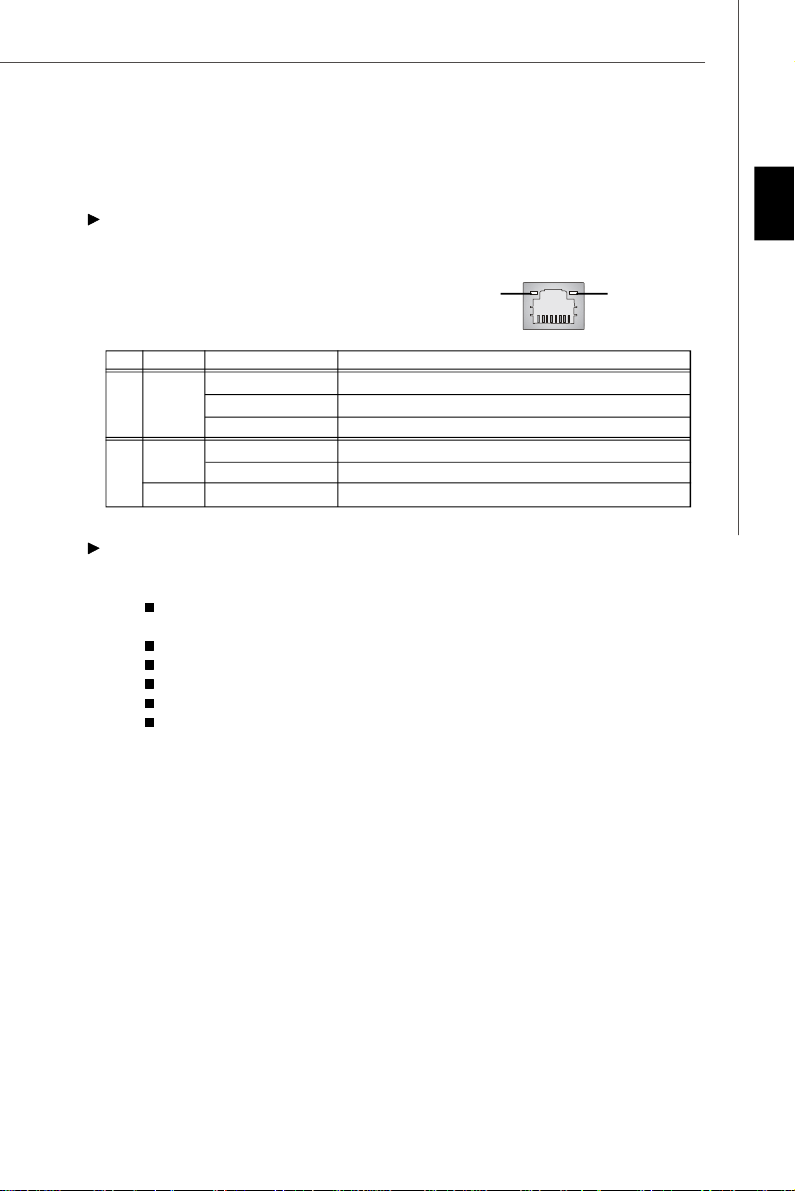
LAN
The standard RJ-45 LAN jack is for connection to the Local Area Network (LAN). You
can connect a network cable to it.
Link IndicatorActivity Indicator
LED Color LED State Condition
Off LAN link is not established.
Left Yellow On (steady state) LAN link is established.
On (brighter & pulsing)The computer is communicating with another computer on the LAN.
Green Off 10 Mbit/sec data rate is selected.
Right On 100 Mbit/sec data rate is selected.
Orange On 1000 Mbit/sec data rate is selected.
Audio Ports
These audio connectors are used for audio devices. You can differentiate the color
of the audio jacks for different audio sound effects.
Line-In (Blue) - Line In is used for external CD player, tapeplayer or other
audio devices.
Line-Out (Green) - Line Out, is a connector for speakers or headphones.
Mic (Pink) - Mic, is a connector for microphones.
RS-Out (Black) - Rear-Surround Out in 4/ 5.1/ 7.1 channel mode.
CS-Out (Orange) - Center/ Subwoofer Out in 5.1/ 7.1 channel mode.
SS-Out (Gray) - Side-Surround Out 7.1 channel mode.
English
En-13
Page 24
MS-7563 Mainboard
Connectors
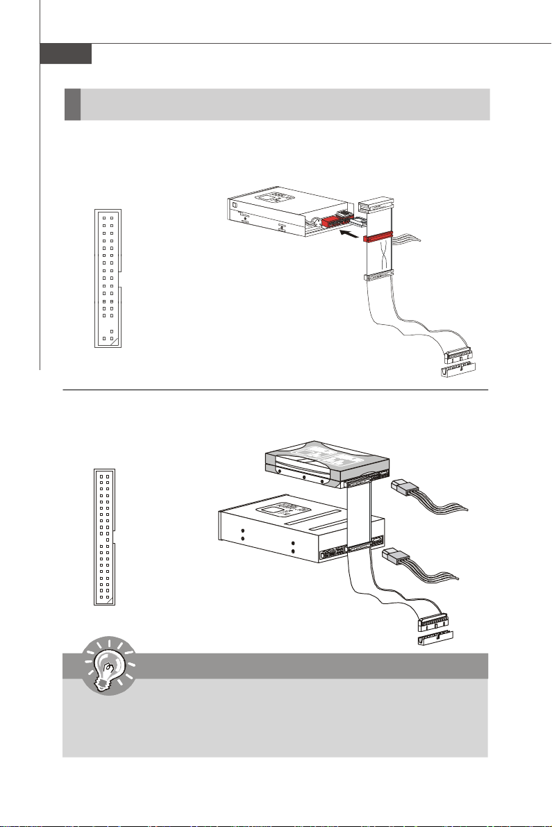
Floppy Disk Drive Connector: FDD1
This connector supports 360KB, 720KB, 1.2MB, 1.44MB or 2.88MB floppy disk drive.
FDD1
IDE Connector: IDE1
This connector supports IDE hard disk drives, optical disk drives and other IDE devices.
IDE1
Important
If you install two IDE devices on the same cable, you must configure the
drives separately to master / slave mode by setting jumpers. Refer to IDE
device’s documentation supplied by the vendors for jumper setting
instructions.
En-14
Page 25
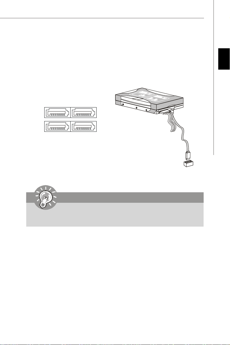
Serial ATA Connector: SATA1 ~ SATA4
This connector is a high-speed Serial ATA interface port. Each connector can connect
to one Serial ATA device.
English
SATA2
SATA1
SATA4
SATA3
Important
Please do not fold the Serial ATA cable into 90-degree angle. Otherwise,
data loss may occur during transmission.
En-15
Page 26
MS-7563 Mainboard
Fan Power Connectors: CPUFAN1, SYSFAN1/2
The fan power connectors support system cooling fan with +12V. When connecting
the wire to the connectors, always note that the red wire is the positive and should
be connected to the +12V; the black wire is Ground and should be connected to GND.
If the mainboard has a System Hardware Monitor chipset on-board, you must use a
specially designed fan with speed sensor to take advantage of the CPU fan control.
GND
+12V
SENSOR
Control
CPUFAN1
SENSOR
+12V
GND
SYSFAN1/2
Important
1.Please refer to the recommended CPU fans at processor’s official website
or consult the vendors for proper CPU cooling fan.
2.CPUFAN1 / SYSFAN1 / SYSFAN2 supports fan control. You can adjust fan
speed in H/W Monitor menu of BIOS and install Dual Core Center utility
that will automatically control the CPU fan speed according to the actual
CPU temperature.
3. Fan cooler set with 3 or 4 pins power connector are both available for
CPUFAN.
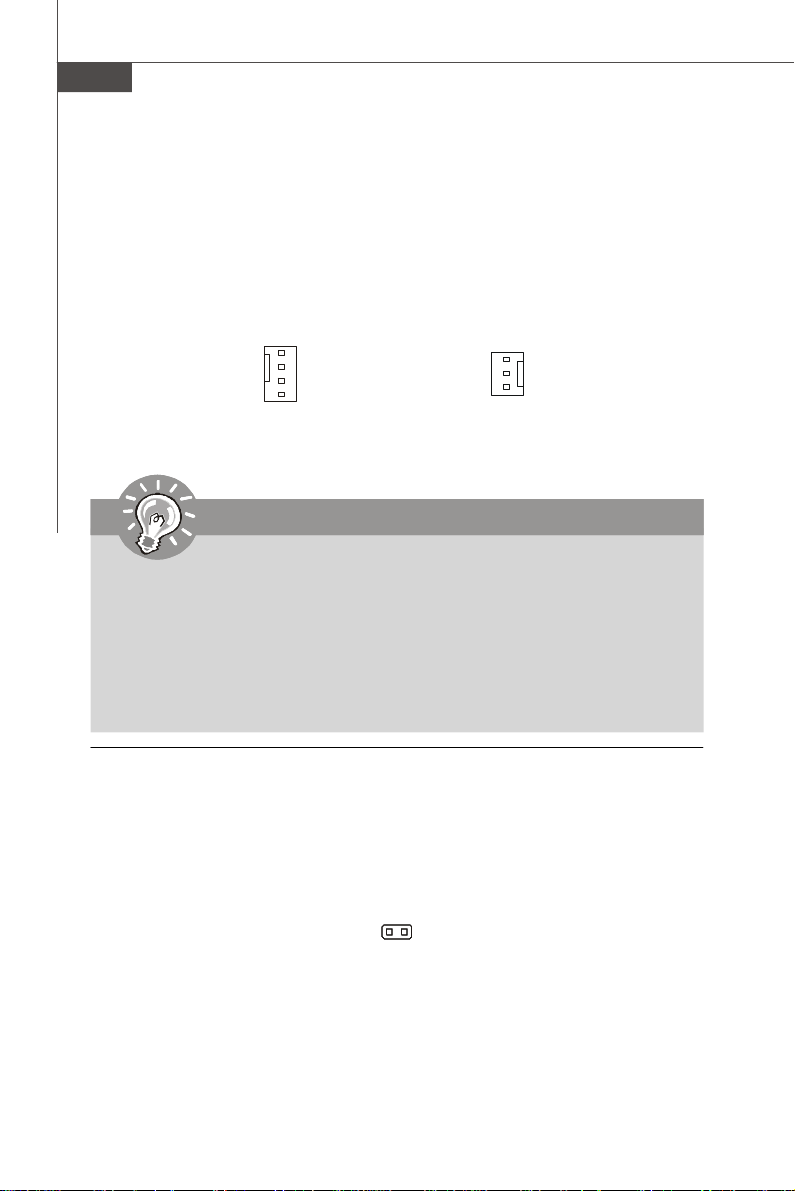
Chassis Intrusion Connector: JCI1
This connector connects to the chassis intrusion switch cable. If the chassis is
opened, the chassis intrusion mechanism will be activated. The system will record
this status and show a warning message on the screen. To clear the warning, you
must enter the BIOS utility and clear the record.
CINTRU
1
JCI1
GND
2
En-16
Page 27
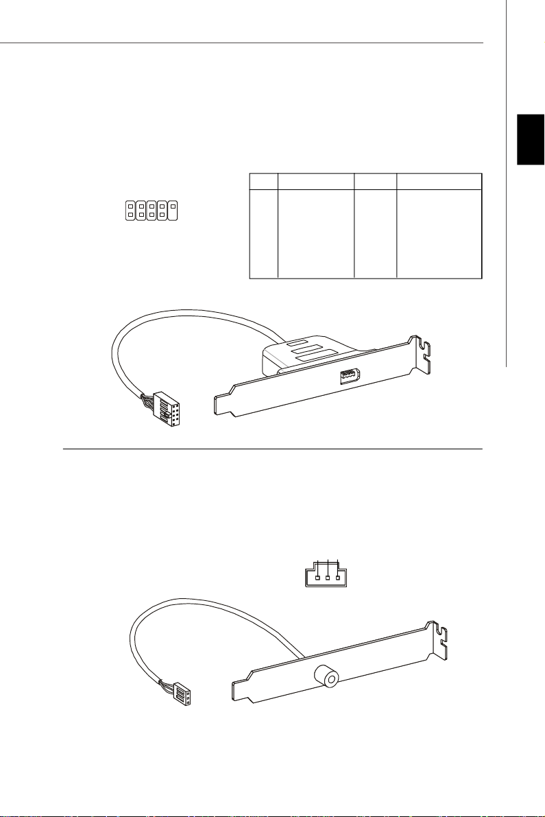
IEEE1394 Connector: J1394_1 (optional)
This connector allows you to connect the IEEE1394 device via an optional IEEE1394
bracket.
Pin Definition
PIN SIGNAL PIN SIGNAL
2
1
J1394_1
(optional)
10
9
1 TPA+ 2 TPA-
3 Ground 4 Ground
5 TPB+ 6 TPB-
7 Cable power 8 Cable power
9 Key (no pin) 10 Ground
IEEE1394 Bracket (Optional)
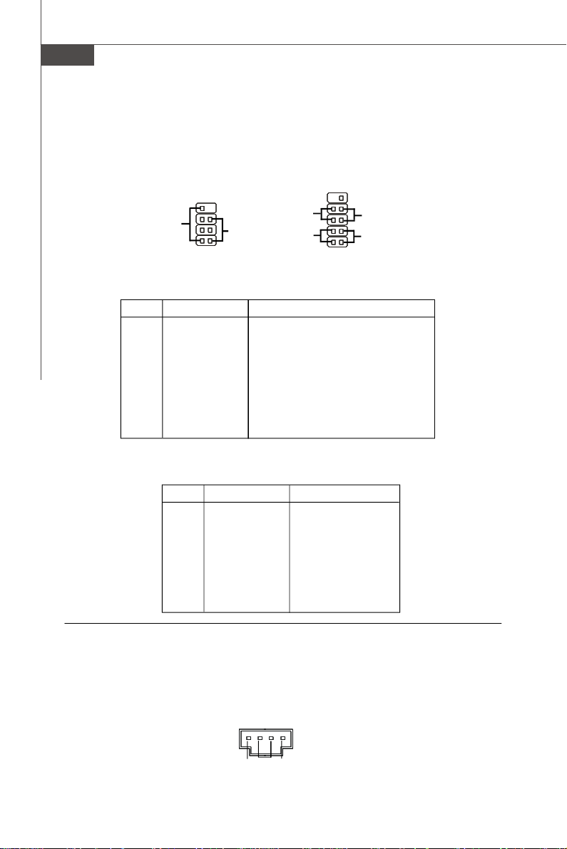
S/PDIF-Out Connector: JSPD1
This connector is used to connect S/PDIF (Sony & Philips Digital Interconnect Format)
interface for digital audio transmission.
English
S
G
P
V
D
N
C
I
C
D
F
JSPD1
S/PDIF Bracket (Optional)
En-17
Page 28
MS-7563 Mainboard
Front Panel Connectors: JFP1, JFP2
These connectors are for electrical connection to the front panel switches and LEDs.
The JFP1 is compliant with Intel® Front Panel I/O Connectivity Design Guide.
Power
Switch++
Power
LED
10
-
JFP1
2
1
9
+
Reset
-
Switch
-
HDD
LED
Speaker
+
-
JFP2
8
+
2
7
Power
LED
1
JFP1 Pin Definition
PIN SIGNAL DESCRIPTION
1 HD_LED + Hard disk LED pull-up
2 FP PWR/SLP MSG LED pull-up
3 HD_LED - Hard disk active LED
4 FP PWR/SLP MSG LED pull-up
5 RST_SW - Reset Switch low reference pull-down to GND
6 PWR_SW + Power Switch high reference pull-up
7 RST_SW + Reset Switch high reference pull-up
8 PWR_SW - Power Switch low reference pull-down to GND
9 RSVD_DNU Reserved. Do not use.
JFP2 Pin Definition
PIN SIGNAL DESCRIPTION
1 GND Ground
2 SPK- Speaker-
3 SLED Suspend LED
4 BUZ+ Buzzer+
5 PLED Power LED
6 BUZ- Buzzer-
7 NC No connection
8 SPK+ Speaker+
CD-In Connector: CD_IN1
This connector is provided for external audio input.
CD_IN1
R
L
GND
En-18
Page 29

Front Panel Audio Connector: JAUD1
This connector allows you to connect the front panel audio and is compliant with
Intel® Front Panel I/O Connectivity Design Guide.
2
1
HD Audio Pin Definition
PIN SIGNAL DESCRIPTION
1 MIC_L Microphone - Left channel
2 GND Ground
3 MIC_R Microphone - Right channel
4 PRESENCE# Active low signal-signals BIOS that a High Definition Audio dongle
5 LINE out_R Analog Port - Right channel
6 MIC_JD Jack detection return from front panel microphone JACK1
7 Front_JD Jack detection sense line from the High Definition Audio CODEC
8 NC No control
9 LINE out_L Analog Port - Left channel
10 LINEout_JD Jack detection return from front panel JACK2
is connected to the analog header. PRESENCE# = 0 when a
High Definition Audio dongle is connected
jack detection resistor network
10
9
JAUD1
TPM Module connector: JTPM1(optional)
This connector connects to a TPM (Trusted Platform Module) module (optional). Please
refer to the TPM security platform manual for more details and usages.
JTPM1
English
13
14
1
2
Pin Signal Description Pin Signal Description
1 LCLK LPC clock 2 3V dual/3V_STB 3V dual or 3V standby power
3 LRST# LPC reset 4 VCC3 3.3V power
5 LAD0 LPC address & data pin0 6 SIRQ Serial IRQ
7 LAD1 LPC address & data pin1 8 VCC5 5V power
9 LAD2 LPC address & data pin2 10 KEY No pin
11 LAD3 LPC address & data pin3 12 GND Ground
13 LFRAME# LPC Frame 14 GND Ground
En-19
Page 30
MS-7563 Mainboard
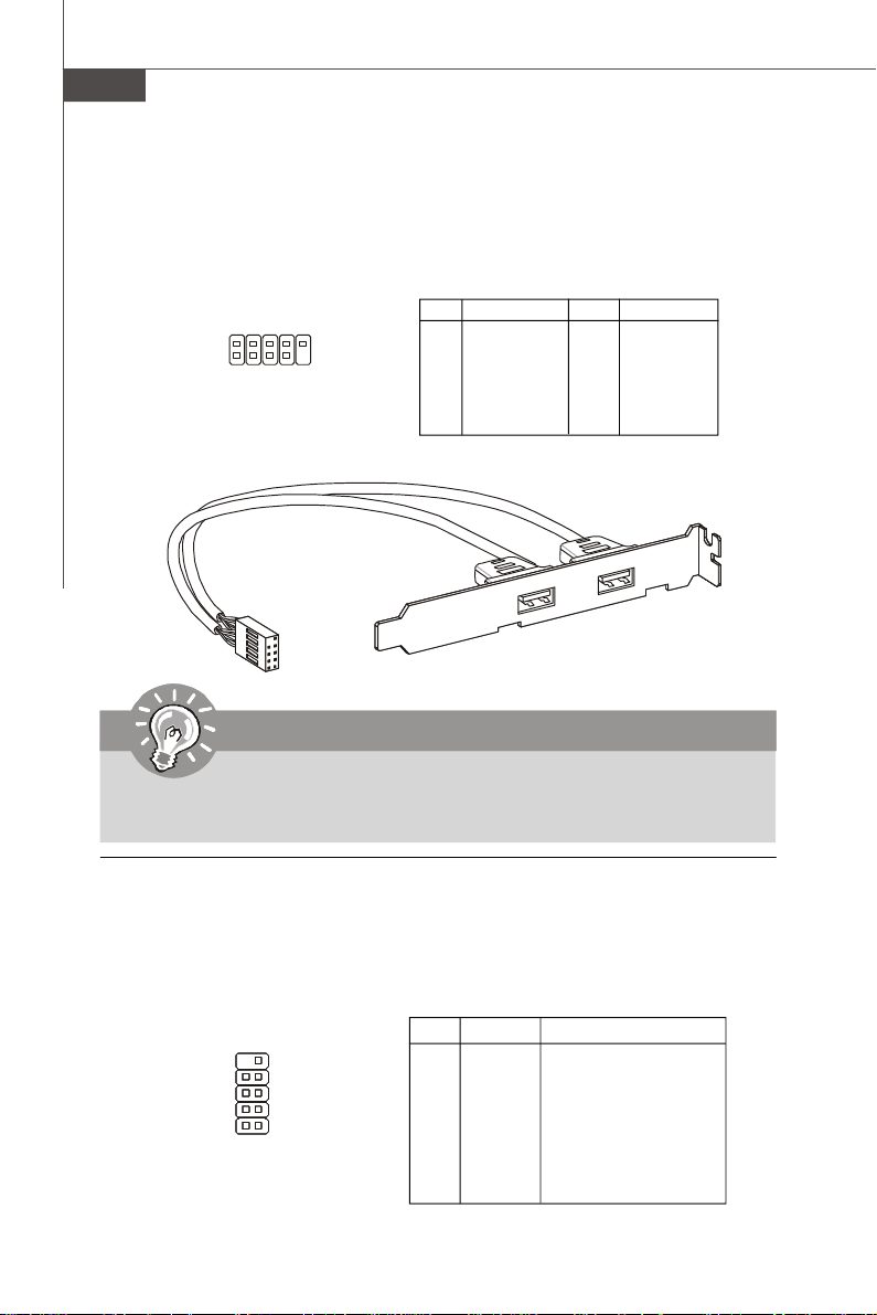
Front USB Connector: JUSB1 ~ 2
These connectors, compliant with Intel® I/O Connectivity Design Guide, is ideal for
connecting high-speed USB interface peripherals such as USB HDD, digital cameras,
MP3 players, printers, modems and the like.
Pin Definition
JUSB1~2
2
1
10
9
PIN SIGNAL PIN SIGNAL
1 VCC 2 VCC
3 USB0- 4 USB1-
5 USB0+ 6 USB1+
7 GND 8 GND
9 Key (no pin) 10 USBOC
USB 2.0 Bracket
(Optional)
Important
Note that the pins of VCC and GND must be connected correctly to avoid
possible damage.
Serial Port Connector: JCOM 1
This connector is a 16550A high speed communication port that sends/receives 16
bytes FIFOs. You can attach a serial device.
Pin Definition
En-20
JCOM1
2
9
1
PIN SIGNAL DESCRIPTION
1 DCD Data Carry Detect
2 SIN Serial In or Receive Data
3 SOUT Serial Out or Transmit Data
4 DTR Data Terminal Ready
5 GND Ground
6 DSR Data Set Ready
7 RTS Request To Send
8 CTS Clear To Send
9 RI Ring Indicate
Page 31

Parallel Port Header: JLPT1
This connector is used to connect an optional parallel port bracket. The parallel port
is a standard printer port that supports Enhanced Parallel Port (EPP) and Extended
Capabilities Parallel Port (ECP) mode.
26 25
JLPT1
2
1
English
PIN SIGNAL PIN SIGNAL
1 RSTB# 2 AFD#
3 PRND0 4 ERR#
5 PRND1 6 PINIT#
7 PRND2 8 LPT_SLIN#
9 PRND3 10 GND
11 PRND4 12 GND
13 PRND5 14 GND
PIN SIGNAL PIN SIGNAL
15 PRND6 16 GND
17 PRND7 18 GND
19 ACK# 20 GND
21 BUSY 22 GND
23 PE 24 GND
25 SLCT 26 Key (No Pin)
En-21
Page 32

MS-7563 Mainboard
Jumper
Clear CMOS Jumper: JBAT1
There is a CMOS RAM onboard that has a power supply from an external battery to
keep the data of system configuration. With the CMOS RAM, the system can automatically boot OS every time it is turned on. If you want to clear the system configuration,
set the jumper to clear data.
JBAT1
1
1 3
Keep Data
1 3
Clear Data
Important
You can clear CMOS by shorting 2-3 pin while the system is off. Then return
to 1-2 pin position. Avoid clearing the CMOS while the system is on; it will
damage the mainboard.
En-22
Page 33

Slots
PCI (Peripheral Component Interconnect) Express Slots
The PCI Express slot supports the PCI Express interface expansion card.
The PCI Express x 16 slot supports up to 4.0 GB/s transfer rate.
The PCI Express x 1 slot supports up to 250 MB/s transfer rate.
PCI Express x16 Slot
PCI Express x1 Slot
PCI (Peripheral Component Interconnect) Slots
The PCI slots support LAN cards, SCSI cards, USB cards, and other add-on cards
that comply with PCI specifications. At 32 bits and 33 MHz, it yields a throughput rate
of 133 MBps.
32-bit PCI Slot
English
Important
When adding or removing expansion cards, make sure that you unplug the
power supply first. Meanwhile, read the documentation for the expansion card
to configure any necessary hardware or software settings for the expansion
card, such as jumpers, switches or BIOS configuration.
En-23
Page 34

MS-7563 Mainboard
PCI Interrupt Request Routing
The IRQ, acronym of interrupt request line and pronounced I-R-Q, are hardware lines
over which devices can send interrupt signals to the microprocessor. The PCI IRQ
pins are typically connected to the PCI bus pins as follows:
Order 1 Order 2 Order 3 Order 4
PCI Slot 1 INT A# INT B# INT C# INT D#
PCI Slot 2 INT B# INT C# INT D# INT A#
En-24
Page 35

BIOS Setup
This chapter provides basic information on the BIOS Setup program and allows you to
configure the system for optimum use. You may need to run the Setup program
when:
* An error message appears on the screen during the system booting up, and requests you to run BIOS SETUP.
* You want to change the default settings for customized features.
Important
1.The items under each BIOS category described in this chapter are under
continuous update for better system performance. Therefore, the description
may be slightly different from the latest BIOS and should be held for reference
only.
2.Upon boot-up, the 1st line appearing after the memory count is the BIOS
version. It is usually in the format:
A7563IMS V1.0 082208 where:
1st digit refers to BIOS maker as A = AMI, W = AWARD, and P = PHOENIX.
2nd - 5th digit refers to the model number.
6th refers to the Chipset vender as A = AMD, I = Intel, V = VIA, N = Nvidia, U =
ULi.
7th - 8th digit refers to the customer as MS = all standard customers.
V1.0 refers to the BIOS version.
082208 refers to the date this BIOS was released.
English
En-25
Page 36

MS-7563 Mainboard
Entering Setup
Power on the computer and the system will start POST (Power On Self Test) process.
When the message below appears on the screen, press <DEL> key to enter Setup.
Press DEL to enter SETUP
If the message disappears before you respond and you still wish to enter Setup,
restart the system by turning it OFF and On or pressing the RESET button. You may
also restart the system by simultaneously pressing <Ctrl>, <Alt>, and <Delete> keys.
Getting Help
After entering the Setup menu, the first menu you will see is the Main Menu.
Main Menu
The main menu lists the setup functions you can make changes to. You can use the
arrow keys (↑↓ ) to select the item. The on-line description of the highlighted setup
function is displayed at the bottom of the screen.
Sub-Menu
If you find a right pointer symbol (as shown in the right view)
appears to the left of certain fields that means a sub-menu
containing additional options can be launched from this field.
You can use control keys (↑↓ ) to highlight the field and
press <Enter> to call up the sub-menu. Then you can use the
control keys to enter values and move from field to field
within a sub-menu. If you want to return to the main menu, just press <Esc >.
General Help <F1>
The BIOS setup program provides a General Help screen. You can call up this screen
from any menu by simply pressing <F1>. The Help screen lists the appropriate keys
to use and the possible selections for the highlighted item. Press <Esc> to exit the
Help screen.
En-26
Page 37

The Main Menu
Once you enter AMI® or AWARD® BIOS CMOS Setup Utility, the Main Menu will appear
on the screen. The Main Menu allows you to select from functions and exit choices.
Use arrow keys to select among the items and press <Enter> to accept or enter the
sub-menu.
Standard CMOS Features
Use this menu for basic system configurations, such as time, date etc.
Advanced BIOS Features
Use this menu to setup the items of AMI® special enhanced features.
Integrated Peripherals
Use this menu to specify your settings for integrated peripherals.
Power Management Setup
Use this menu to specify your settings for power management.
H/W Monitor
This entry shows your PC health status.
BIOS Setting Password
Use this menu to set the password for BIOS.
Cell Menu
Use this menu to specify your settings for frequency/voltage control and overclocking.
Load Fail-Safe Defaults
Use this menu to load the default values set by the BIOS vendor for stable system
performance.
Load Optimized Defaults
Use this menu to load the default values set by the mainboard manufacturer specifically for optimal performance of the mainboard.
Save & Exit Setup
Save changes to CMOS and exit setup.
Exit Without Saving
Abandon all changes and exit setup.
English
En-27
Page 38

MS-7563 Mainboard
When enter the BIOS Setup utility, follow the processes below for general use.
1. Load Optimized Defaults : Use control keys (↑↓) to highlight the Load Opti-
mized Defaults field and press <Enter> , a message as below appears:
Select [Ok] and press Enter to load the default settings for optimal system
performance.
2. Setup Date/ Time : Select the Standard CMOS Features and press <Enter> to
enter the Standard CMOS Features-menu. Adjust the Date, Time fields.
3. Save & Exit Setup : Use control keys (↑↓) to highlight the Save & Exit Setup
field and press <Enter> , a message as below appears:
Select [Ok] and press Enter to save the configurations and exit BIOS Setup utility.
Important
The configuration above are for general use only. If you need the detailed
settings of BIOS, please see the manual in English version on MSI website.
En-28
Page 39

4. Cell Menu Introduction : This menu is for advanced user who want to overclock
the mainboard.
Important
Change these settings only if you are familiar with the chipset.
Current CPU / DRAM Frequency
These items show the current clocks of CPU and Memory speed. Read-only.
English
Intel EIST
The Enhanced Intel SpeedStep technology allows you to set the performance level of
the microprocessor whether the computer is running on battery or AC power. This
field will appear after you installed the CPU which support speedstep technology.
Adjust CPU FSB Frequency (MHz)
This item allows you to set the CPU FSB frequency (in MHz).
Adjusted CPU Frequency (MHz)
It shows the adjusted CPU frequency (FSB x Ratio). Read-only.
Advance DRAM Configuration
Press <Enter> to enter the sub-menu.
En-29
Page 40

MS-7563 Mainboard
Configure DRAM Timing by SPD
Setting to [Enabled] enables DRAM CAS# Latency automatically to be determined
by BIOS based on the configurations on the SPD (Serial Presence Detect) EEPROM
on the DRAM module.
CAS Latency(CL)
When the Configure DRAM Timing by SPD sets to [Manual], the field is
adjustable.This controls the CAS latency, which determines the timing delay (in
clock cycles) before SDRAM starts a read command after receiving it.
tRCD
When the Configure DRAM Timing by SPD sets to [Manual], the field is
adjustable. When DRAM is refreshed, both rows and columns are addressed
separately. This setup item allows you to determine the timing of the transition
from RAS (row address strobe) to CAS (column address strobe). The less the
clock cycles, the faster the DRAM performance.
tRP
When the Configure DRAM Timing by SPD sets to [Manual], this field is
adjustable. This setting controls the number of cycles for Row Address Strobe
(RAS) to be allowed to precharge. If insufficient time is allowed for the RAS to
accumulate its charge before DRAM refresh, refresh may be incomplete and
DRAM may fail to retain data. This item applies only when synchronous DRAM is
installed in the system.
tRAS
When the Configure DRAM Timing by SPD sets to [Manual], this setting determines the time RAS takes to read from and write to a memory cell.
tRTP
When the Configure DRAM Timing by SPD sets to [Manual], this setting controls the time interval between a read and a precharge command.
tRFC
When the Configure DRAM Timing by SPD sets to [Manual], the field is
adjustable. The row cycle time determines the minimum number of clock cycles
a memory row takes to complete a full cycle, from row activation up to the
precharging of the active row.
tWR
When the Configure DRAM Timing by SPD sets to [Manual], the field is
adjustable. It specifies the amount of delay (in clock cycles) that must elapse
after the completion of a valid write operation, before an active bank can be
precharged. This delay is required to guarantee that data in the write buffers
can be written to the memory cells before precharge occurs.
tRRD
When the Configure DRAM Timing by SPD sets to [Manual], the field is
adjustable. Specifies the active-to-active delay of different banks.
En-30
Page 41

tWTR
When the Configure DRAM Timing by SPD sets to [Manual], the field is
adjustable. This item controls the Write Data In to Read Command Delay memory
timing. This constitutes the minimum number of clock cycles that must occur
between the last valid write operation and the next read command to the same
internal bank of the DDR device.
FSB/Memory Ratio
This item will allow you to adjust the FSB/Ratio of the memory.
Adjusted DRAM Frequency (MHz)
It shows the adjusted DDR Memory frequency. Read-only.
Adjust PCI-E Frequency (MHz)
This field allows you to select the PCIE frequency (in MHz).
Auto Disable DIMM/PCI Frequency
When set to [Enabled], the system will remove (turn off) clocks from empty DIMM and
PCI slots to minimize the electromagnetic interference (EMI).
CPU Voltage(V)/ CPU GTL REF(V)/ Memory Voltage(V)/ Momory REF(V)/ NB
Voltage(V)/ VTT FSB Voltage(V)
These items are used to asjust the voltage of CPU, Memory and chipset.
Spread Spectrum
When the motherboard’s clock generator pulses, the extreme values (spikes) of the
pulses create EMI (Electromagnetic Interference). The Spread Spectrum function
reduces the EMI generated by modulating the pulses so that the spikes of the pulses
are reduced to flatter curves. If you do not have any EMI problem, leave the setting at
Disabled for optimal system stability and performance. But if you are plagued by EMI,
set to Enabled for EMI reduction. Remember to disable Spread Spectrum if you are
overclocking because even a slight jitter can introduce a temporary boost in clock
speed which may just cause your overclocked processor to lock up.
English
Important
1.If you do not have any EMI problem, leave the setting at [Disabled] for
optimal system stability and performance. But if you are plagued by EMI,
select the value of Spread Spectrum for EMI reduction.
2.The greater the Spread Spectrum value is, the greater the EMI is reduced,
and the system will become less stable. For the most suitable Spread
Spectrum value, please consult your local EMI regulation.
3.Remember to disable Spread Spectrum if you are overclocking because
even a slight jitter can introduce a temporary boost in clock speed which
may just cause your overclocked processor to lock up.
En-31
Page 42

MS-7563 Mainboard
Software Information
Take out the Driver/Utility CD that is included in the mainboard package, and place it into
the CD-ROM drive. The installation will auto-run, simply click the driver or utility and
follow the pop-up screen to complete the installation. The Driver/Utility CD contains
the:
Driver menu - The Driver menu shows the available drivers. Install the driver by your
desire and to activate the device.
Utility menu - The Utility menu shows the software applications that the mainboard
supports.
WebSite menu- The WebSite menu shows the necessary websites.
Important
Please visit the MSI website to get the latest drivers and BIOS for better
system performance.
En-32
Page 43

G41M
시리즈
사용 설명서
한국어
한국어
Kr-1
Page 44

MS-7563
메인보드
메인보드 사양
지원되는 프로세서
- LGA775
프로세서
-
팬 속도 컨트롤이 있는 4핀
(CPU에 대한 최신
cpuform2 참조)
패키지의
Intel Core 2 Quad/Core 2 Duo/Yorkeld/ Wolfdale
CPU
팬 핀 헤더 지원
http://global.msi.com.tw/index.php?func=
정보는
지원되는
- 1333/ 1066/ 800 MHz
칩셋
- 노스
-
지원되는 메모리
- DDR2 667/800 SDRAM(
- DDR2 DIMMs (240핀/1.8V) 2
LAN
- Realtek 8111D
오디오
- Realtek ALC888에 의해
- 잭 감지
- Vista Premium
IDE
- ICH7에 의한 IDE 포트 1
- Ultra DMA 66/100 모드
- PIO, 버스
SATA
- ICH7
- 최대 3 Gb/s의 저장 및
플로피
-
- 360KB, 720KB, 1.2MB, 1.44MB 및 2.88MB의 FDD 1개
FSB
: Intel G41
브릿지
사우스 브릿지
(호환
index.php?func=testreport를
에 의한
플로피 포트 1개
: Intel ICH7
가능한 부품에 대한 자세한 내용은
기능이 있는 플렉시블 8채널 오디오
마스터 작동 모드 지원
SATA 포트 4
칩셋
L에 의해
적합성 지원
10/100/1000
개
지원
데이터 전송 지원
칩셋
최대
통합된 칩
개
8GB)
개
참조하십시오
고속 이더넷 지원
http://global.msi.com.tw/
.)
지원
Kr-2
커넥터
후면 패널
- PS/2
마우스 포트 1개
- PS/2
키보드 포트 1개
Page 45

- VGA
포트 1개
- DVI-D 포트 1
- DisplayPort 잭 1
- USB 2.0 포트 4
- 1 RJ-45 LAN
- 1394
-
플렉시블 오디오 잭 6개
개
개
개
잭
포트 1개(옵션
)
온보드 핀헤더/커넥터
- USB 2.0
- CD
- SPDIF
- IEEE 1394
-
전면 패널 오디오 핀헤더 1개
-
직렬 포트 핀헤더 1개
핀헤더 2개
입력 핀헤더 1개
출력 핀헤더 1개
핀헤더 1개(옵션
)
- TPM 1개(옵션)
-
섀시 침입 스위치 핀헤더 1개
-
병렬 포트 핀헤더 1개
슬롯
- PCI Express x16 슬롯 1
- PCI Express x1 슬롯 1
- PCI
슬롯 2개
- 3.3V/5V PCI 버스
개
개
인터페이스 지원
폼 팩터
- Micro- ATX (24.4cm X 22.8cm)
장착
- 장착 구멍 6
개
한국어
Kr-3
Page 46

MS-7563
메인보드
빠른 부품 설명서
후면 패널,
Kr-12
PCIE,
Kr-23
PCI,
Kr-23
SYSFAN1,
Kr-16
CD_IN1,
Kr-18
JAUD1,
Kr-19
JPW1,
Kr-11
J1394_1,
Kr-17
JSPD1,
Kr-17
CPU,
Kr-5
JUSB1/2,
Kr-20
CPUFAN1,
Kr-16
JFP1/2,
Kr-18
JCI1,
Kr-16
JBAT1,
Kr-22
ATX1,
Kr-11
DDR2,
Kr-9
FDD1,
Kr-14
JLPT1,
Kr-21
JTPM1,
Kr-19
JCOM1,
Kr-20
SYSFAN2,
Kr-16
IDE1,
Kr-14
SATA1~4,
Kr-15
Kr-4
Page 47

CPU (
중앙 처리 장치
)
CPU 설치 시
컴퓨터를 켜기 전에 판매점에 문의하십시오
CPU에 대한 최신
과열을 방지하는 쿨러를 반드시 설치하십시오
http://global.msi.com.tw/index.php?func=cpuform2
정보는
.
. CPU
쿨러가 없는 경우
중요 사항
과열
CPU와
과열은
록 냉각 팬이 제대로 작동하는지 항상 확인하십시오. 열이 잘 발산되도록
와 방열판 사이에 서멀 페이스트(또는 서멀 테이프)를 고르게 바르십시오
CPU
교체
CPU 교체 시, 항상
된 콘센트에서 뽑아
오버클로킹
이 메인보드는 오버클로킹 기능을 지원하도록 디자인되었습니다. 그러나 오버
클로킹이 진행되는 동안 부품이 이러한 비정상적인 설정을 견뎌낼 수 있는지 확
인하십시오. 제품 사양을 초과하는 범위에서 작동시키지 마십시오. 당사는 올바
르지 않은 작동이나 제품 사양을 초과한 범위에서 사용하여 발생한 손상 또
는 위험은 보증하지 않습니다.
LGA 775 CPU
LGA 775 CPU의 핀 패드 면
시스템을 심각하게 손상시킬 수 있습니다
전원을 끄거나 먼저
CPU의
안전을 확보하십시오
ATX 전원
소개
LGA 775 CPU의 표면.
열이 잘 발산되도록 서멀 페이스
트를 표면에 약간 바르십시오
. CPU가
공급장치의 전원 코드를 접지
.
과열되지 않도
참조
.
.
,
한국어
CPU
정렬 키
노란색 삼각형은 핀 1의 표시기입니다
정렬 키
.
노란색 삼각형은 핀 1의 표시기입니다
.
Kr-5
Page 48

MS-7563
CPU
및 쿨러 설치
CPU 설치 시
록 방열판/쿨러 팬을 설치하기 전에
단계에 따라
가 손상됩니다
메인보드
과열을 방지하는 쿨러를 상단에 연결하십시오. 한편, 열이 잘 발산되도
CPU 및
쿨러를 올바로 설치하십시오. 잘못 설치할 경우
.
CPU에 서멀
페이스트를 약간 바르십시오. 아래의
CPU와
메인보드
1. CPU
3.
소켓에는 접촉에 의한 손상을
방지하는 플라스틱 캡이 있습니다
CPU를
설치하기 전에, 항상 캡으로
소켓을 덮어 소켓 핀을 보호하십시오
소켓의 핀이 드러납니다
.
2.
.
.
화살표와 같이 캡을 레버 힌지 쪽으
로부터 제거하십시오
4. 로드
레버를 엽니다
.
.
1.
시스템을 켜기 전에
2.
손상을 방지하려면
3. CPU
Kr-6
중요 사항
CPU
쿨러가 단단히 설치되었는지 확인합니다
CPU
랜드쪽 커버의 가용성은
소켓을 만지지 마십시오
CPU
패킹에 따라 다릅니다
.
.
.
Page 49

5. 로드
레버를 위로 올리고 로드 플
레이트를 엽니다
7. CPU
가 소켓에 제대로 앉혀졌는지
.
육안으로 검사합니다. 그렇지 않은
CPU
경우,
를 수직 방향으로 들어
올린 다음 다시 설치합니다.
6. CPU
방향이 올바로 맞춰졌는지 확
인한 다음,
레임에 내려 놓습니다.
CPU
를 소켓 하우징 프
CPU
스의 가장자리를 잡으십시오. 정렬
키가 맞춰졌는지 유의하십시오.
정렬 키
8.
로드 플레이트로 패키지를 덮습니
다.
베이
한국어
Kr-7
Page 50

MS-7563
메인보드
9.
로드 레버를 로드 플레이트 위로 살
짝 누른 다음, 리텐션 탭 아래의 훅
을 사용하여 레버를 고정합니다.
11. 4
개의 훅을 눌러 쿨러를 고정합니다.
그리고 나서 잠금 스위치를 돌려 훅
을 잠급니다(스위치에 표시된 올바
른 방향 참조).
10.
메인보드의 구멍을 방열판과 맞춥
. 4개의
니다
클립이 메인보드의 구
멍에 완전히 박힐 때까지 쿨러를 누
.
릅니다
12.
메인보드를 뒤집어 클립 엔드가 올
바로 끼워졌는지 확인합니다
메인보드
.
잠금 스위치
훅
중요 사항
1. BIOS에서 CPU
2. CPU가
틱 캡으로
3. 이 절에
상태를 읽습니다
설치되어 있지 않은 경우, 손상되지 않도록 (그림 1과 같이) 항상 플라스
CPU 소켓 핀을
표시된 메인보드 사진은
사진입니다. 메인보드의 외양은 구입한 모델에 따라 다를 수 있습니다
Kr-8
.
보호하십시오
CPU/쿨러
.
설치를 보여줄 목적으로만 사용된
.
Page 51

메모리
DIMM
슬롯은 메모리 모듈을 설치하는 데 사용됩니다
호환 가능한 부품에 대한 자세한 내용은
port
를 참조하십시오
.
DDR2
240-핀, 1.8V
56x2=112
http://global.msi.com.tw/index.php?func=testre
핀
.
64x2=128
핀
듀얼 채널 모드 배포 규칙
듀얼 채널 모드에서는 메모리 모듈이 2개의 데이터 버스 회선을 동시에 사용하여 데이
터를 전송 및 수신할 수 있습니다. 듀얼 채널 모드를 활성화하면 시스템 성능이 향상
됩니다. 다음 그림에서 듀얼 채널 모드의 배포 규칙을 참조하십시오.
DIMM1
DIMM2
비어 있음
설치됨
한국어
Kr-9
Page 52

MS-7563
메인보드
메모리 모듈 설치
1.
메모리 모듈은 중앙에 노치가 하나만 있으며, 오른쪽 방향으로만 맞습니다
2.
메모리 모듈을
핑거가
, DIMM
으면
DIMM
DIMM
슬롯의 양쪽에 있는 플라스틱 클립이 자동으로 닫힙니다
슬롯에 수직으로 끼웁니다. 그리고 나서 메모리 모듈 위의 골든
슬롯에 깊이 삽입될 때까지 밀어 넣습니다. 메모리 모듈이 제자리를 잡
중요 사항
메모리 모듈이
3.
메모리 모듈이 양쪽에 있는
확인하십시오
DIMM
슬롯에 제대로 삽입되면 골든 핑거가 거의 보이지 않습니다
.
DIMM 슬롯
볼트
클립에 의해 제자리에 잠가졌는지 수동으로
노치
.
.
.
중요 사항
- DDR2
메모리 모듈은
지 않습니다. 항상
- 듀얼 채널
듈을 설치했는지 확인하십시오
-
성공적인 시스템 부팅을 하려면, 메모리 모듈을 먼저
모드에서, 다른 채널
Kr-10
DDR과 서로
DDR2 DIMM
교환되지 않으며
DDR2
슬롯에
DIMM
슬롯에 유형과 밀도가 동일한 메모리 모
.
, DDR2
메모리 모듈을 설치해야 합니다
표준은 역호환이 되
DIMM1에
끼우십시오
.
.
Page 53

전원 공급장치
ATX 24
핀 전원 커넥터
이 커넥터를 사용하여
ATX 24핀 전원
공급장치를 연결하려렴, 전원 공급장치의 플러그가 올
: ATX1
ATX 24핀 전원
공급장치를 연결할 수 있습니다
바른 방향으로 삽입되었는지, 핀이 정렬되었는지 확인하십시오. 그리
고 나서 전원 공급장치를 커넥터 안쪽으로 꽉 맞게 누릅니다
원하는 경우
ATX 전원
13과 함께
핀
ATX1
ATX 12V
12V
20핀 ATX 전원
공급장치를 사용할 수 있습니다
공급장치를 사용하려면, 전원 공급장치의 플러그를 핀
연결하십시오(오른쪽 이미지 참조
12
1
전원 커넥터
전원 커넥터는
JPW1
24
13
핀 신호
1 +3.3V
2 +3.3V
3 GND
4 +5V
5 GND
6 +5V
7 GND
8 PWR OK
9 5VSB
10 +12V
11 +12V
12 +3.3V
: JPW1
CPU
에 전원을 공급하는 데 사용됩니다.
2
4
1
3
).
핀 정의
핀 신호
1 GND
2 GND
3 12V
4 12V
.
. 20핀
1 및
핀 신호
13 +3.3V
14 -12V
15 GND
16 PS-ON#
17 GND
18 GND
19 GND
20 Res
21 +5V
22 +5V
23 +5V
24 GND
핀 정의
13
핀
.
핀
12
한국어
중요 사항
1.
모든 커넥터가 올바른
적인지 확인하십시오
2.
시스템 안정성을 위해
3. ATX 12V
전원 연결은
ATX 전원
.
350와트
18A
보다 커야 합니다
공급장치에 연결되어 메인보드의 작동이 안정
이상의 전원 공급장치를 권장합니다
.
.
Kr-11
Page 54

MS-7563
메인보드
후면 패널
1394
포트
마우스
키보드
PCIE x16
는 어떤 신호도 출력하지 않습니다.
마우스/키보드
PS/2
표준
VGA
포트
DB15
핀 피메일 커넥터가 모니터용으로 제공됩니다
DVI-D
DVI-D (Digital Visual Interface-Digital)
습니다. 이 커넥터는 컴퓨터와 디스플레이 장치를 고속의 디지털 방식으로 연결합니다
LCD
모니터를 연결하려면, 모니터 케이블을
끝이 모니터에 제대로 연결되었는지 확인하기만 하면 됩니다
설명서를 참조하십시오
VGA 포트
DVI-D 포트
중요 사항
중요 사항
슬롯에 확장 카드가 삽입되어 있으면,
®
마우스/키보드
포트
DIN
.)
DisplayPort
커넥터는
커넥터를 사용하여
(옵션)
VGA, DisplayPort
PS/2®
마우스/키보드용입니다
.
DVI
커넥터에 연결하고 케이블의 다른 쪽
USB 포트 마이크
LCD
라인 입력
LAN
라인 출력
DVI-D
및
.
모니터를 연결할 수 있
. (
자세한 내용은 모니터
RS 출력
CS 출력
SS 출력
포트
.
USB
포트
USB(Universal Serial Bus)
USB
같은
DisplayPort
playPort
후면 패널의
장치를 연결하는 데 사용됩니다
DisplayPor
1394 포트(옵션)
t
는 디지털 디스플레이 인터페이스 표준입니다. 이 커넥터는 모니터를
입력장치에 연결하는 데 사용됩니다.
IEEE1394
포트는
Kr-12
포트는 키보드, 마우스 또는 기타
IEEE1394
.
장치에 대한 연결을 제공합니다
USB
호환 가능 장치와
.
Dis-
Page 55

LAN
표준 RJ-45 LAN 잭은 Local Area Network(LAN) 연결용입니다. 네트워크 케이블을 이
잭에 연결할 수 있습니다.
활동 표시등
링크 표시등
LED 칼라 LED 상태 조건
꺼짐 LAN 링크가 구축되지 않았습니다.
왼쪽 노란색 켜기(지속 상태) LAN 링크가 구축되었습니다.
켜기(밝게 및 펄싱)
녹색 꺼짐 10 Mbit/sec 데이터 속도를 선택했습니다.
오른쪽
켜짐 100 Mbit/sec 데이터 속도를 선택했습니다.
오렌지 켜짐 1000 Mbit/sec 데이터 속도를 선택했습니다.
컴퓨터가 LAN 상의 다른 컴퓨터와 통신 중입니다.
오디오 포트
이 오디오 커넥터는 오디오 장치에 사용됩니다. 오디오 잭의 색상으로 오디오 사운드
효과를 구별할 수 있습니다.
라인 입력(파란색) - 라인 입력은 외부 CD 플레이어, 테이프 플레이어 또
는 기타 오디오 장치에 사용됩니다.
라인 출력(녹색) - 라인 출력은 스피커 또는 헤드폰에 사용되는 커넥터입
니다.
마이크(핑크색) - 마이크는 마이크에 사용되는 커넥터입니다.
RS 출력(검은색) - 4/5.1/7.1 채널 모드의 뒤쪽 서라운드 출력.
CS 출력(오렌지색) - 5.1/7.1 채널 모드의 중앙/서브우퍼 출력.
SS 출력(회색) - 7.1 채널 모드의 측면 서라운드 출력.
한국어
Kr-13
Page 56

MS-7563
커넥터
메인보드
플로피 디스크 장치 커넥터:
이 커넥터는
지원합니다
IDE
이 커넥터는
합니다
360KB, 720KB, 1.2MB, 1.44MB 또는 2.88MB
.
FDD1
.
IDE1
IDE 하드
디스크 드라이브, 광학 디스크 드라이브 및 기타
커넥터:
FDD1
플로피 디스크 드라이브를
IDE
장치를 지원
IDE1
중요 사항
동일한 케이블에 2개의
이브에 드라이브를 별도로 구성해야 합니다. 점퍼 설정 방법은 공급업체가 제공
IDE
한
장치의 설명서를 참조하십시오
Kr-14
IDE
장치를 설치하는 경우, 점퍼 설정으로 마스터/슬레
.
Page 57

ATA
직렬
이 커넥터는 고속의 직렬
ATA
커넥터:
장치에 연결할 수 있습니다
SATA1~SATA4
ATA
인터페이스 포트에 사용됩니다. 각 커넥터는 하나의 직렬
.
한국어
SATA2
SATA1
ATA
직렬
수 있습니다
중요 사항
케이블을
.
SATA4
SATA3
90도로 꺾지
마십시오. 그럴 경우, 전송 중 데이터가 손실될
Kr-15
Page 58

MS-7563
메인보드
팬 전원 커넥터:
팬 전원 커넥터는
상 빨간색 전선이 양극으로서
GND에
연결되어야 합니다. 메인보드에 시스템 하드웨어 모니터 칩셋 온보드가 있는 경
, CPU 팬
우
니다
제어를 활용하기 위해 속도 센서가 있는 특별히 디자인된 팬을 사용해야 합
.
CPUFAN1, SYSFAN1/2
+12V의
시스템 냉각 팬을 지원합니다. 전선을 커넥터에 연결할 때, 항
+12V에
GND
+12V
센서
컨트롤
연결되어야 하고, 검은색 전선은 접지선으로서
CPUFAN1
센서
+12V
GND
SYSFAN1/2
중요 사항
1.
프로세서의 공식 웹 사이트에서 권장
CPU 냉각 팬을
문의하십시오
2. CPUFAN1/SYSFAN1/SYSFAN2
터 메뉴에서 팬 속도를 조정하고 실제
으로 제어하는
3. 3 또는 4핀 전원
습니다
Dual Core Center
커넥터로 설치된 팬 쿨러는 모두
.
CPU 팬을
참조하거나 판매점에 올바른
.
는 팬 제어를 지원합니다
CPU
온도에 따라
유틸리티를 설치할 수 있습니다
CPUFAN에서
. BIOS의 H/W
CPU
팬 속도를 자동
모니
.
사용할 수 있
섀시 침입 커넥터
: JCI1
이 커넥터는 섀시 침입 스위치 케이블에 연결됩니다. 섀시가 열리는 경우, 섀시 침입 메
커니즘이 활성화됩니다. 시스템이 이 상태를 기록하고 화면에 경고 메시지를 표시합니다
경고를 지우려면
, BIOS
유틸리티에서 레코드를 지워야 합니다
CINTRU
GND
1
2
.
JCI1
Kr-16
.
Page 59

IEEE1394
커넥터
: J1394_1 (
이 커넥터를 사용하여 옵션인
.
습니다
2
1
10
9
J1394_1
(옵션)
옵션
IEEE1394
)
브래킷을 통해
핀 신호 핀 신호
1 TPA+ 2 TPA-
3
5 TPB+ 6 TPB-
7
9
IEEE1394
핀 정의
4
접지
케이블 전원
) 10
키(핀 없음
8
장치를 연결할 수 있
접지
케이블 전원
접지
한국어
S/PDIF
출력 커넥터
: JSPD1
이 커넥터는 디지털 오디오 전송을 위해
Format)
인터페이스를 연결하는 데 사용됩니다
S/PDIF
IEEE1394
브래킷(옵션
)
S/PDIF(Sony & Philips Digital Interconnect
.
SPDIF
GND
VCC
JSPD1
브래킷(옵션
)
Kr-17
Page 60

MS-7563
메인보드
전면 패널 커넥터:
JFP1, JFP2
이 커넥터는 전면 패널 스위치 및 LED에 대한 전기 연결에 사용됩니다.
Front Panel I/O Connectivity Design Guide
JFP2
8
7
+
-
스피커
-
핀 신호 설명
1 HD_LED + 하드 디스크 LED 풀업
2 FP PWR/SLP MSG LED 풀업
3 HD_LED - 하드 디스크 활성화 LED
4 FP PWR/SLP MSG LED 풀업
5 RST_SW - 리셋 스위치 낮은 기준 GND로 풀다운
6 PWR_SW + 전원 스위치 높은 기준 풀업
7 RST_SW + 리셋 스위치 높은 기준 풀업
8 PWR_SW - 전원 스위치 낮은 기준 GND로 풀다운
9 RSVD_DNU 예약됨. 사용하지 않음.
핀 신호 설명
1 GND 접지
2 SPK- 스피커3 SLED 일시 중단 LED
4 BUZ+ 부저+
5 PLED 전원 LED
6 BUZ- 부저7 NC 연결 없음
8 SPK+ 스피커+
전원
+
LED
2
1
JFP1
JFP2
핀 정의
핀 정의
를 준수합니다.
JFP1
10
전원
-
스위치
+
전원
LED
2
1
9
+
-
-
+
HDD
LED
리셋
스위치
JFP1은 Intel
®
CD
입력 커넥터
: CD_IN1
이 커넥터는 외부 오디오 입력용으로 제공됩니다.
CD_IN1
L
R
GND
Kr-18
Page 61

전면 패널 오디오 커넥터:
JAUD1
(옵션)
이 커넥터를 사용하여 전면 패널 오디오를 연결할 수 있으며, 이 커넥터는
Panel I/O Connectivity Design Guide
를 준수합니다
.
Intel® Front
TPM
모듈 커넥터
이 커넥터는
사용법은
TPM 보안
JTPM1
14
2
1
HD
오디오 핀 정의
핀 신호 설명
1 MIC_L 마이크 – 왼쪽 채널
2 GND 접지
3 MIC_R 마이크 – 오른쪽 채널
4 PRESENCE# 활성화된 낮은 신호 - BIOS에게 고음질 오디오 동글이 아날
5 라인 출력_R 아날로그 포트 – 오른쪽 채널
6 마이크_JD 전면 패널 마이크 JACK1에서 잭 감지 반환
7 전면_JD 고음질 오디오 코덱 잭 감지 레지스터 네트워크로부터의 잭 감
8 NC 컨트롤 없음
9 라인 출력_L 아날로그 포트 – 왼쪽 채널
10 라인 출력_JD 전면 패널 JACK2에서 잭 감지 반환
: JTPM1
(옵션)
TPM(Trusted Platform Module) 모듈(옵션)에
플랫폼 설명서를 참조하십시오
13
10
JAUD1
9
로그 헤더에 연결되었다고 알립니다. PRESENCE# = 고음질
오디오 동글이 연결된 경우 0
지 센서 라인
연결됩니다. 자세한 내용과
.
한국어
1
2
핀 신호 설명 핀 신호 설명
1 LCLK LPC 클록 2 3V 듀얼/3V_STB 3V 듀얼 또는 3V 대기 전원
3 LRST# LPC 리셋 4 VCC3 3.3V 전원
5 LAD0 LPC 주소 및 데이터 핀 0 6 SIRQ 직렬 IRQ
7 LAD1 LPC 주소 및 데이터 핀 1 8 VCC5 5V 전원
9 LAD2 LPC 주소 및 데이터 핀 2 10 키 핀 없음
11 LAD3 LPC 주소 및 데이터 핀 3 12 GND 접지
13 LFRAME# LPC 프레임 14 GND 접지
Kr-19
Page 62

MS-7563
메인보드
USB
전면
커넥터
Intel® I/O Connectivity Design Guide를
: JUSB1~2
준수한 이 커넥터는
MP3 플레이어, 프린터, 모뎀 등과 같은 고속의
는 데 적합합니다
.
핀 신호
JUSB1~2
2
1
10
9
1 VCC 2 VCC
3 USB0- 4 USB1-
5 USB0+ 6 USB1+
7 GND 8 GND
9
중요 사항
VCC 및 GND의 핀은
손상을 방지하기 위해 올바로 연결되어야 합니다
USB HDD
USB
인터페이스 주변 장치를 연결하
핀 정의
) 10 USBOC
키(핀 없음
USB 2.0 브래킷
, 디지털 카메라,
핀 신호
(옵션)
.
직렬 포트 커넥터
: JCOM1
이 커넥터는 16550A 고속 통신 포트로서 16 바이트의 FIFO를 송수신합니다. 직렬 장
치를 연결할 수 있습니다.
핀 정의
JCOM1
2
9
1
핀 신호 설명
1 DCD 데이터 이동 감지
2 SIN 직렬 입력 또는 데이터 수신
3 SOUT 직렬 출력 또는 데이터 전송
4 DTR 데이터 단말기 준비
5 GND 접지
6 DSR 데이터 세트 준비
7 RTS 송신 요청
8 CTS 송신 지우기
9 RI 발신음 표시
Kr-20
Page 63

병렬 포트 헤더:
JLPT1
이 커넥터는 옵션인 병렬 포트 브래킷을 연결하는 데 사용됩니다. 병렬 포트는 표준
프린터 포트로서, 확장 병렬 포트(EPP) 및 확장 성능 병렬 포트(ECP) 모드를 지원합
니다.
25
26
JLPT1
1
2
한국어
핀 신호 핀 신호
1 RSTB# 2 AFD#
3 PRND0 4 ERR#
5 PRND1 6 PINIT#
7 PRND2 8 LPT_SLIN#
9 PRND3 10 GND
11 PRND4 12 GND
13 PRND5 14 GND
핀 신호 핀 신호
15 PRND6 16 GND
17 PRND7 18 GND
19 ACK# 20 GND
21 BUSY 22 GND
23 PE 24 GND
25 SLCT 26 키(핀 없음)
Kr-21
Page 64

MS-7563
점퍼
메인보드
CMOS
점퍼 지우기
보드에 시스템 구성 데이터를 유지하기 위해 외부 배터리로부터 전원을 공급 받은
CMOS RAM
동으로 부팅합니다. 시스템 구성을 지우려면, 점퍼를 설정하여 데이터를 지우십시오.
이 있습니다.
JBAT1
1
: JBAT1
CMOS RAM
의 경우, 시스템을 켤 때마다 시스템이 OS를 자
3
1
데이터 유지
1 3
데이터 지우기
중요 사항
시스템이 꺼져 있는 동안
1-2
나서
핀 위치로 돌아가십시오. 시스템이 켜 있는 동안에는
2-3
핀을 단락시켜
마십시오. 그럴 경우 메인보드가 손상될 수 있습니다.
CMOS
를 지울 수 있습니다. 그리고
CMOS
를 지우지
Kr-22
Page 65

슬롯
PCI (Peripheral Component Interconnect) Express
PCI Express
PCI Express x 16은 최대 4.0 GB/s의
PCI Express x 1은 최대 250 MB/s의
PCI (Peripheral Component Interconnect)
PCI
를 지원합니다
LAN 카드, SCSI 카드, USB 카드 및 PCI
슬롯은
슬롯은
. 32
비트 및
PCI Express
PCI Express x1 슬롯
33 MHz
인터페이스 확장 카드를 지원합니다
전송률을 지원합니다
전송률을 지원합니다
.
.
PCI Express x16
슬롯
규격을 준수하는 기타 애드온 카드
에서는 처리량 속도가
133 MBps
32비트 PCI
슬롯
슬롯
.
입니다
한국어
슬롯
.
중요 사항
확장 카드를 추가하거나 제거할 때 먼저 전원 공급장치의 플러그를 뽑으십시오
점퍼, 스위치 또는
트웨어 설정을 구성하려면 확장 카드의 설명서를 읽으십시오
BIOS
구성과 같은 확장 카드에 대해 필요한 하드웨어 및 소프
.
Kr-23
.
Page 66

MS-7563
PCI
인터럽트 요청 라우팅
Interrupt request line의
이크로프로세서로 전송할 수 있는 하드웨어 회선입니다
음과 같이
메인보드
PCI 버스 핀에
IRQ는 I-R-Q라고
약어인
연결됩니다
발음하며, 장치가 인터럽트 신호를 마
.
. PCI IRQ 핀은
일반적으로 다
1
PCI 슬롯 1 INT A# INT B# INT C# INT D#
PCI 슬롯 2 INT B# INT C# INT D# INT A#
순서
순서
2
순서
3
순서
4
Kr-24
Page 67

BIOS
설정
이 장에서는 BIOS 설정 프로그램에 대한 기본 정보를 제공하여 사용자가 최적의 사용
을 위해 시스템을 구성할 수 있도록 도와줍니다. 다음의 경우 설정 프로그램을 실행해
야 합니다.
* 시스템을 부팅하는 동안 화면에 오류 메시지가 나타나고 BIOS 설정을 실행하도록 요
청하는 경우.
* 사용자 정의된 기능을 사용하기 위해 기본 설정을 변경하려는 경우.
중요 사항
1.
이 장에서 설명되는 각
계속적으로 업데이트됩니다. 따라서 설명이 최신
조용으로만 사용해야 합니다.
2.
부팅 시 메모리 카운트 다음에 나타나는 첫 번째 행의 정보가
다.이는 대개의 경우 다음과 같은 형식으로 표시됩니다.
1
번째 문자는
2~5
번째 자리수는 모델 번호입니다
6
번째 문자는 칩셋 공급업체로서
ULi
입니다
7~8
번째 문자는 고객으로서
V1.0은 BIOS
082208
.
은 이
BIOS
버전입니다
BIOS
BIOS
범주 아래의 항목은 시스템 성능을 향상하기 위해
A7563IMS V1.0 082208,
마커로서
가 발표된 날짜입니다
, A = AMI, W = AWARD, P = PHOENIX
.
, A = AMD, I = Intel, V = VIA, N = Nvidia, U =
, MS =
.
모든 표준 고객입니다
BIOS
와 약간 다를 수 있으며 참
BIOS
버전입니
여기에서
.
.
입니다
.
한국어
Kr-25
Page 68

MS-7563
메인보드
설정 시작
컴퓨터를 켜면 시스템이
래의 메시지가 표시되면
사용자가 응답하거나 설정을 입력하기 전에 메시지가 표시되면, 시스템을 껐다가 다시
켜거나 리셋
를 동시에 눌러 시스템을 다시 시작할 수도 있습니다
도움말 불러오기
설정 메뉴를 시작한 다음, 처음으로 표시되는 메뉴가 주 메뉴입니다
주 메뉴
주 메뉴는 변경할 수 있는 설정 기능을 나열합니다. 화살표 키
선택할 수 있습니다. 강조 표시된 설정 기능의 온라인 설명이 화면의 하단에 표시됩니다
하위 메뉴
오른쪽 그림과 같이 올바른 포인터 기호가 특정 필드의 왼쪽에
표시되면, 이 필드에서 추가 옵션을 포함한 하위 메뉴를 시작할
수 있다는 것을 의미합니다. 컨트롤 키
강조 표시하고
나서 컨트롤 키를 사용하여 값을 입력하고 하위 메뉴 내에서 필
드 간을 이동합니다. 주 메뉴로 돌아가려면
하면 됩니다
일반 도움말
BIOS 설정
어느 메뉴에서든지 이 화면을 불러낼 수 있습니다. 도움말 화면은 사용할 수 있는 적절
한 키와 강조 표시된 항목에 대해 선택할 수 있는 항목을 나열합니다
도움말 화면이 종료됩니다
(RESET)
<Enter>를 눌러 하위
.
<F1>
프로그램은 일반 도움말 화면을 제공합니다. 간단히
POST(Power On Self Test)
, <DEL> 키를 눌러
DEL
을 눌러 설정
버튼을 눌러 다시 시작합니다. 또한
.
설정을 시작합니다
(SETUP)
(↑↓) 를
메뉴를 불러냅니다. 그리고
, <Esc >를
프로세스를 시작합니다. 화면에 아
을 시작합니다
.
사용하여 필드를
.
.
<Ctrl>, <Alt> 및 <Delete>
.
(↑↓)를
사용하여 항목을
누르기만
<F1>을
. <Esc>를
누르기만 하면
키
누르면
.
Kr-26
Page 69

주 메뉴
AMI® 또는 AWARD® BIOS CMOS 설정 유틸리티에 들어가면 주 메뉴가 화면에 표시됩니
다. 주 메뉴의 설정 기능 및 종료 방법 중에서 선택할 수 있습니다. 화살표 키를 사용하여
항목 중 하나를 선택한 다음 <Enter>를 눌러 하위 메뉴를 수락하거나 또는 시작합니다.
Standard CMOS Features (표준 CMOS 기능)
이 메뉴를 사용하여 시간, 날짜 등과 같은 기본 시스템 구성을 처리합니다.
Advanced BIOS Features (고급 BIOS 기능)
이 메뉴를 사용하여 AMI® 특별 고급 기능의 항목을 설정합니다.
Integrated Peripherals (통합된 주변 장치)
이 메뉴를 사용하여 통합된 주변 장치의 설정을 지정합니다.
Power Management Setup (전원 관리 설정)
이 메뉴를 사용하여 전원 관리의 설정을 지정합니다.
H/W Monitor (H/W 모니터)
이 항목은 PC의 상태를 표시합니다.
BIOS Setting Password (BIOS 설정 암호)
이 메뉴를 사용하여 BIOS의 암호를 설정합니다.
Cell Menu (셀 메뉴)
이 메뉴를 사용하여 주파수/전압 제어 및 오버클로킹의 설정을 지정합니다.
Load Fail-Safe Defaults (장애시 안전 기본값 로드)
이 메뉴를 사용하여 안정된 시스템 성능을 위해 BIOS 공급업체가 설정한 기본값을 로
드합니다.
Load Optimized Defaults (최적 기본값 로드)
이 메뉴를 사용하여 특별히 메인보드 최적의 성능을 위해 메인보드 제조업체가 설정한
기본값을 로드합니다.
Save & Exit Setup (저장 및 설정 종료)
CMOS에 변경사항을 저장하고 설정을 종료합니다.
Exit Without Saving (저장하지 않고 종료)
모든 변경사항을 취소하고 설정을 종료합니다.
한국어
Kr-27
Page 70

MS-7563
BIOS
설정 유틸리티를 시작할 때, 일반적 사용의 경우 다음 절차를 따르십시오.
1. Load Optimized Defaults (
Optimized Defaults (
같은 메시지가 표시됩니다
메인보드
최적 기본값 로드
최적 기본값 로드)를 선택한 다음
.
):
컨트롤 키
(↑↓)를
<Enter>를
사용하여
Load
누르면 아래와
[OK(확인)]을
이 로드됩니다
2. Setup Date/ Time (
을 선택한 다음
필드를 조정합니다
3. Save & Exit Setup (
Setup (
메시지가 표시됩니다
[OK(확인)] 키와 Enter 키를 눌러
이제
료합니다
선택하고
.
날짜/시간 설정
<Enter>를
.
저장 및 설정 종료) 필드를 강조표시한 다음
.
중요 사항
[Enter(엔터)]를
눌러서 표준
저장 및 설정 종료
.
누르면 최적의 시스템 성능을 위한 기본 설정
): Standard CMOS Features (표준 CMOS 기능)
구성을 저장한 다음
CMOS 기능
):
컨트롤 키
메뉴로 들어갑니다. 날짜, 시간
(↑↓)를
사용하여
<Enter>를
BIOS 설정
Save & Exit
누르면 아래와 같은
유틸리티를 종
위의 구성은 일반적 사용의 경우에만 해당됩니다
MSI
은
웹사이트의 한국어 설명서를 참조하십시오
Kr-28
. BIOS
설정에 대한 자세한 내용
.
Page 71

4. Cell Menu Introduction (셀 메뉴 소개):
를 위한 메뉴입니다
.
중요 사항
메인보드를 오버클로킹하려는 고급 사용자
한국어
주파수
.
) (MHz)
.
)
방식으로 컴퓨터를
) (MHz)
.
전용입니다
사용자가 칩셋에 익숙할 경우에만 이 설정을 변경하십시오
Current CPU / DRAM Frequency (현재 CPU / DRAM
이 항목은
향상된
실행되느냐에 따라 마이크로프로세서의 성능 레벨을 설정할 수 있습니다
기술을 지원하는
이 항목을 사용하여
이 항목은 조정된
<Enter>
CPU 및
Intel EIST
Intel SpeedStep
Adjust CPU FSB Frequency (MHz) (CPU FSB
Adjusted CPU Frequency (MHz) (CPU
Advance DRAM Conguration (고급 DRAM 구성)
를 눌러 하위 메뉴를 시작합니다
메모리 속도의 현재 클록을 표시합니다. 읽기 전용입니다
기술로 인해 배터리 또는
CPU를
설치하면 이 필드가 표시됩니다
CPU FSB
CPU
주파수를 표시합니다
주파수
(MHZ)를
.
AC 전원 중 어떤
주파수 조정
설정할 수 있습니다
주파수 조정
(FSB x 비율). 읽기
.
. speedstep
.
Kr-29
Page 72

MS-7563
Congure DRAM Timing by SPD (SPD를 사용한 DRAM 타이밍 구성)
[Enabled (사용)]으로 설정하면 DRAM 모듈의 SPD(직렬 존재 감지) EFPROM 구성을
기준으로 하는 BIOS에 의해 DRAM CAS# 대기 시간(DRAM CAS# Latency)을 자동 판
별할 수 있습니다.
CAS Latency(CL) (CAS 대기 시간)
Congure DRAM Timing by SPD (SPD를 사용한 DRAM 타이밍 구성) 을 [Manual(수
동)]으로 설정하면, 필드를 조정할 수 있습니다. 이렇게 되면 SDRAM이 읽기 명령을 받
아서 이 명령을 시작하기 전에 (클록 사이클의) 타이밍 지연을 결정하는 CAS 대기 시
간을 제어합니다
tRCD
Congure DRAM Timing by SPD (SPD를 사용한 DRAM 타이밍 구성) 을 [Manual(수
동)]으로 설정하면, 필드를 조정할 수 있습니다. DRAM이 재충전되면 행과 열이 따로 분
리됩니다. 이 설정 항목을 사용하면 RAS(열 주소)에서 CAS(행 주소)로의 변환 타이밍을
결정할 수 있습니다. 클록 사이클이 짧을수록 DRAM 성능이 빨라집니다.
tRP
Congure DRAM Timing by SPD (SPD를 사용한 DRAM 타이밍 구성) 을 [Manual(수
동)]으로 설정하면, 필드를 조정할 수 있습니다. 이 설정은 사전에 충전할 수 있는 RAS
사이클 수를 제어합니다. DRAM 재충전 이전에 RAS가 충전 시간을 충분히 갖지 못할
경우, 충전이 불충분해서 DRAM이 데이터를 보존하지 못할 수 있습니다. 이 항목은 시
스템에 동기화 DRAM이 설치된 경우에만 적용됩니다.
tRAS
Congure DRAM Timing by SPD (SPD를 사용한 DRAM 타이밍 구성) 이 [Manual(수
동)]으로 설정되어 있는 경우, 이 설정은 RFC가 메모리 셀로부터 읽거나 메모리 셀에
쓰는 데 걸리는 시간을 결정합니다.
메인보드
tRTP
Congure DRAM Timing by SPD (SPD를 사용한 DRAM 타이밍 구성) 이 [Manual(수
동)]으로 설정되어 있는 경우, 이 설정은 읽기 명령과 사전 충전 사이의 시간 간격을 제
어합니다.
tRFC
Congure DRAM Timing by SPD (SPD를 사용한 DRAM 타이밍 구성) 을 [Manual(수
동)]으로 설정하면, 필드를 조정할 수 있습니다. 행 사이클 시간은 메모리 행이 행 활성
화에서 현재 행의 사전 충전에 이르기까지 전체 사이클을 완료하는 데 필요한 클럭 사
이클의 최소 수를 결정합니다.
tWR
Congure DRAM Timing by SPD (SPD를 사용한 DRAM 타이밍 구성) 을 [Manual(수
동)]으로 설정하면, 필드를 조정할 수 있습니다. 유효한 쓰기 작업의 완료 후 현재 뱅크
를 사전 충전할 수 있을 때까지 경과해야 하는 클럭 사이클의 지연을 지정합니다. 이
지연은 사전 충전이 발생하기 전에 쓰기 버퍼의 데이터를 메모리 셀에 쓸 수 있도록 하
는 데 필요합니다.
tRRD
Congure DRAM Timing by SPD (SPD를 사용한 DRAM 타이밍 구성) 을 [Manual(수
동)]으로 설정하면, 필드를 조정할 수 있습니다. 다른 뱅크의 active-to-active 지연을 지
정합니다.
Kr-30
Page 73

tWTR
Conguration DRAM Timing by SPD (SPD를 사용한 DRAM 타이밍 구성)
을 [Manual(수동)]으로 설정하면, 필드를 조정할 수 있습니다. 이 항목은 읽기 명령
지연에 데이터 쓰기(Write Data In to Read Command Delay) 메모리 타밍을 제어합
니다. 이 항목이 DDR 장치의 동일한 내부 뱅크에 대한 유효한 최종 쓰기 작업과 다
음 읽기 명령 사이에 발생하는 클럭 사이클의 최소 수를 구성합니다.
FSB/Memory Ratio (FSB/메모리 비율)
이 항목을 사용하면 FSB/메모리 비율을 조정할 수 있습니다.
Adjusted DRAM Frequency (MHz) (DRAM 주파수 조정) (MHz)
이 항목은 DDR 메모리 주파수를 표시합니다. 읽기 전용입니다.
Adjust PCI-E Frequency (MHz) (PCI-E 주파수 조정) (MHz)
이 항목을 사용하여 PCIE 주파수(MHZ)를 선택할 수 있습니다.
Auto Disable DIMM/PCI Frequency (DIMM/PCI 주파수 자동 해제)
[Enabled (사용)]으로 설정하면 시스템이 빈 DIMM 및 PCI 슬롯에서 클록을 제거(전원이
꺼짐)하여 전자파 장애(EMI)를 최소화할 수 있습니다.
CPU Voltage(V)/ CPU GTL REF(V)/ Memory Voltage(V)/ Momory REF(V)/ NB
Voltage(V)/ VTT FSB Voltage(V) (CPU 전압(V)/ CPU GTL REF(V)/ 메모리 전압(V)/ 메
모리 REF(V)/ NB 전압(V)/ VTT FSB 전압(V))
이 항목은 CPU, 메모리 및 칩셋의 전압 조정에 사용됩니다.
Spread Spectrum (대역 확산)
메인보드의 클록 생성기가 펄스화되면 펄스의 극치값(스파이크)이 전자파 장애를 일으
킵니다. 대역 확산 기능은 펄스 조절로 생성된 EMI를 줄여줌으로써 그 결과 펄스의 스
파이크가 평탄한 곡선으로 줄어듭니다. EMI 문제가 발생하지 않을 경우 최적의 시스템
안정성 및 성능을 위해 사용 안함으호 설정합니다. 그러나 EMI로 인해 문제가 발생할
경우 EMI 감소를 사용으로 설정하십시오. 사소한 지터조차도 클록 속도를 일시적으로
상승시키면 오버클로킹한 프로세스를 고정시키는 원인이 될 수 있으므로 오버클로킹을
진행하는 동안 대역 확산을 반드시 사용 안함으로 설정해야 합니다.
한국어
중요 사항
1. EMI
문제가 발생하지 않을 경우 최적의 시스템 안정성 및 성능을 위해 [사용
안함]으로 설정합니다. 그러나
위해 대역 확산 값을 선택하십시오.
2.
대역 확산 값이 클수록
장 적합한 대역 확산 값은 해당 지역의
3.
사소한 지터조차도 클록 속도를 일시적으로 상승시키면 오버클로킹한 프로
세스를 고정시키는 원인이 될 수 있으므로 오버클로킹을 진행하는 동안 대역
확산을 반드시 사용 안함으로 설정해야 합니다.
EMI
로 인해 문제가 발생할 경우
EMI
는 감소되지만 시스템의 안정성은 저하됩니다. 가
EMI
규정을 참조하십시오.
EMI
감소를
Kr-31
Page 74

MS-7563
메인보드
소프트웨어 정보
메인보드 패키지에 들어 있는 드라이버/유틸리티 CD를 꺼내서 CD-ROM 드라이브에 삽
입합니다. 설치는 자동 실행되며, 드라이버나 유틸리티를 클릭하기만 하면 팝업 화면이
설치 완료를 표시합니다. 드라이버/유틸리티 CD에는 다음이 포함됩니다.
드라이버 메뉴 – 사용 가능한 드라이버를 표시합니다. 원하는 대로 드라이버를 설치한
유틸리티 메뉴 – 메인보드가 지원하는 소프트웨어 응용 프로그램을 표시합니다.
웹사이트 메뉴 – 필요한 웹사이트를 표시합니다.
다음 장치를 활성화합니다.
중요 사항
최신 드라이버 및
문하십시오.
Kr-32
BIOS
로 시스템 성능을 향상시키고 싶다면
MSI
웹사이트를 방
Page 75

G41M
シリーズ
取扱説明書
日 本 語
日本語
Jp-1
Page 76

MS-7563 マザーボード
マザーボードの仕様
プロセッサー
- LGA775 Intel® Core 2 Quad/ Core 2 Duo/ / Yorkfield/ Wolfdaleプロ
セッサーをサポート
- ファン回転コントロール付けの4ピンCPUファンピンヘッダーをサポー
ト
(最新のCPU対応の詳細については弊社のホームページを参照してくださ
い。 http://global.msi.com.tw/index.php?func=cpuform2)
対応FSB
- 1333/ 1066/ 800 MHz
チップセット
- ノースブリッジ: Intel® G41チップセット
- サウスブリッジ: Intel® ICH7チップセット
メモリ
- DDR2 667/800 SDRAM (最大8GB搭載可)
- 2 DDR2 DIMMs (240ピン / 1.8V)
(最新のメモリモジュール対応表は下記のホームページをご参照くださ
い。http://global.msi.com.tw/index.php?func=testreport)
LAN
- Realtek 8111DL 10/100/1000ファーストイーサネット
オーディオ
- Realtek® ALC888
-ジャックセンス付けの8チャンネル
- Vista premium準拠
IDE
- 1 IDEポート(ICH7)
- Ultra DMA 66/100モードをサポート
- PIO, バスマスターなどのオペレーションモードをサポート
SATA
- 4 SATA ポート(ICH7)
- 最大3 Gb/sまでのデータ転送速度をサポート
フロッピー
- 1 フロッピポート
- 360KB/720KB/1.2MB/1.44MB/2.88MBのFDD、1台の接続が可能
コネクター
バックパネル
- 1 PS/2 マウスポート
- 1 PS/2 キーボードポート
Jp-2
Page 77

- 1 VGA ポート
- 1 DVI-D ポート
- 1 DisplayPortジャック
- 4 USB 2.0 ポート
- 1 RJ-45 LAN ジャック
- 1 1394 ポート(オプション)
- 6 オーディオジャック
オンボードピンヘッダー/コネクター
- 2 USB 2.0 ピンヘッダー
- 1 CD-in ピンヘッダー
- 1 SPDIF-Out ピンヘッダー
- 1 IEEE 1394 ピンヘッダー(オプション)
- 1 フロントパネルオーディオピンヘッダー
- 1 シリアルポートピンヘッダー
- 1 TPM (オプション)
- 1 ケース開放センサーコネクター
- 1 パラレルポートピンヘッダー
スロット
- PCI Express x16 -1スロット
- PCI Express x 1 -1スロット
- PCI -2スロット
- 3.3V/ 5V PCIバスインターフェイスをサポート
寸法
- Micro-ATX (24.4cm X 22.8cm)
取付穴
- 6 穴
日 本 語
Jp-3
Page 78

MS-7563 マザーボード
クイックコンポーネントガイド
Back Panel,
Jp-12
PCIE,
Jp-23
PCI,
Jp-23
SYSFAN1,
Jp-16
JAUD1,
Jp-19
JSPD1,
Jp-17
CD_IN1,
Jp-18
JPW1,
Jp-11
J1394_1,
Jp-17
CPU,
Jp-5
JUSB1/2,
Jp-20
CPUFAN1,
Jp-16
JFP1/2,
Jp-18
JCI1,
Jp-16
JBAT1,
Jp-22
ATX1,
Jp-11
DDR2,
Jp-9
FDD1,
Jp-14
JLPT1,
Jp-21
JTPM1,
Jp-19
JCOM1,
Jp-20
SYSFAN2,
Jp-16
IDE1,
Jp-14
SATA1~4,
Jp-15
Jp-4
Page 79

CPUに関する注意事項
CPUをインストールする場合には、過熱を防止するために、必ずクーラーを取
り付けて下さい。CPUクーラーが取り付けられていない時は、ヒートシングと
冷却ファンを購入し、取り付けてからコンピューターの電源を投入してくだ
さい。
最新のCPU対応表は下記のホームページからご参照ください。
http://global.msi.com.tw/index.php?func=cpuform2
注意!
過熱
CPUが適切に冷却されず、過剰に発熱すると、CPUが破損する場合があ
ります。組み立て後の最初の起動の際に、冷却ファンが正常に動作す
ることを必ず確認してください。
CPUの交換
CPUを交換する場合は必ずコンセントからATX電源コードを抜いた後に
行ってください。通電中のCPUの交換はCPUの破損を招くだけでなく、
感電する危険性があります。
LGA 775 CPUについて
LGA 775 CPUの端子側
Alignment Key Alignment Key
LGA 775 CPUの正面
必要に応じてシリコングリス
を塗布してください。
日 本 語
黄色い矢印マークが指した方向をピ
ン1の方向に向けて装着します。
黄色い矢印マークが指した方向をピ
ン1の方向に向けて装着します。
Jp-5
Page 80

MS-7563 マザーボード
CPU&クーラーの装着
CPUを取り付ける場合には、オーバーヒートを防ぐためにヒートシンクとクー
ラーをCPUに密着するように確実に取り付けてください。また、ヒートシンク
をCPUに装着する場合には必ず必要に応じてシリコングリスを塗布してくださ
い。下記の手順に従って正しくCPUとCPUクーラーを装着してください。装着
方法を誤ると最悪の場合はCPUやマザーボードなどの破損を招きます。
1.CPUのランドサイドカバー( 端子
保護カバー)を外します。
3.CPUソケットのピンが露出した
状態になります。
2. ソ ケットレバー側からソケット
保護カバーをゆっくり外しま
す。
4. レバーを固定プレートのフック
から外します。
注意!
1.システムを起動する前にCPUクーラーがしっかり装着されることを確認
してください。
2.損傷を防ぐために、CPU裏面のpinには決して触れないでください。
3.CPUランドサイドカバーの利用可能はCPUのパッキングで決まられます。
Jp-6
Page 81

5. レバーと固定プレートを起こ
します。
6.CPUのalignment key(位置決めの
窪み) とCPUソケットの[出っ張
り] を 合わせて、装着する向き
を決定します。
位置決めの窪み
日 本 語
7.CPUが正しくソケットに収まっ
ていることを確認してください
8. 固定プレートをゆっくり下ろ
します。
Jp-7
Page 82

MS-7563 マザーボード
9. レバーを下ろしてフックに固定
します。
11. 位置が正しいことを確認したら、
フックが固定されるまでプッシュ
ピン押し込みます。
10. CPUクーラーの四隅のピンをマ
ザーボードの固定穴に合わせ、
ゆっくりと押し込みます。
12. マ ザ ーボードを裏返して、裏面
に出たプッシュピンの先が開き、
正しくロックできたことを 確認し
ます。
マザーボード
locking
switch
フック
注意!
1.使用するCPUにBIOSが対応していることを確認して下さい。
2.ソケットに添付されるプラスチックカバーは捨てないでください。CPU
を外して保管する場合は、このプラスチックカバーを装着し、ソケッ
トのピンを保護してください。
3.本節の図はCPU/クーラーの取付説明用のためにお手元のマザーボードと
は細部が異なる場合があります。
Jp-8
Page 83

メモリ
Installed
1
これらのDIMMスロットはメモリモジュールのインストール用です。
最新のメモリモジュール対応表は下記のホームページを参照ください。
http://global.msi.com.tw/index.php?func=testreport
DDR2
240-pin, 1.8V
64x2=128 pin56x2=112 pin
デュアルチャンネルメモリソケットルール
デュアルチャンネルメモリアクセス方式は、二つのメモリデータバスを同時
に使用してデータの読み書きを行うことになり、アクセススピードを向上さ
せます。デュアルチャンネルを有効にするには、以下の組み合わせでメモリ
モジュールを装着します。
DIMM1
DIMM2
Empty
日 本 語
Jp-9
Page 84

MS-7563 マザーボード
メモリモジュールの装着
1.メモリモジュールは中央に一つだけの切れ欠きが設けられており、このた
め、間違った向きでは差し込めないようになっています。
2. DIMMメモリモジュールをDIMMスロットに垂直に差込ます。DIMMスロットの両
側にあるクラスチップクリップが自動的に固定します。
注意!
手応えが固くてうまの差し込めない場合は無理に力を入れず、左右が傾
かないよう水平を保った状態でゆっくり押し込んでください。
3.手動でメモリモジュールが両側のDIMMスロットクリップに正しくロックされたか
どうか をチェックしてください。
出っ張り 切り欠き
注意!
- DDR2メモリとDDRメモリは互いに規格の互換性がありません。本製品ではDDRモ
ジュールを使用することはできません。
- デュアルチャンネルアクセスで有効にするには同一のメモリを2本装着してください。
-メモリスロットはDIMM1を優先的に使用してください。
Jp-10
Page 85

電源
ATX 24ピン電源コネクター: ATX1
ATX電源24ピンコネクタを接続します。接続の際にはコネク
ターの向きに注意して奥までしっかり差し込んでください。
通常はコネクターのフックの向きを合わせれば正しく接続さ
れます。20ピンのATX電源も使用可能です。その場合には、
11, 12, 23 & 24ピンは使用しません。(右側の図を参照して下
さい)
Pin Definition
PIN SIGNAL
13 +3.3V
14 -12V
15 GND
16 PS-ON#
17 GND
18 GND
19 GND
20 Res
21 +5V
22 +5V
23 +5V
24 GND
ATX1
12
1
24
13
PIN SIGNAL
1 +3.3V
2 +3.3V
3 GND
4 +5V
5 GND
6 +5V
7 GND
8 PWR OK
9 5VSB
10 +12V
11 +12V
12 +3.3V
ATX 12V電源コネクター: JPW1
この 電源コネクターは、CPUに電源を供給します。
Pin Definition
PIN SIGNAL
1 GND
2 GND
3 12V
4 12V
JPW1
2
4
1
3
pin 13
pin 12
日 本 語
注意!
1. 本製品を動作させるためにコネクターは正しいATX電源に接続することを
確認してください。
2. 350W以上の良質な電源ユニットを使用してください。
3. ATX 12Vラインは18A以上供給できる電流を使用してください。。
Jp-11
Page 86

MS-7563 マザーボード
バックパネル
マウス
キーボード
VGAポート
DVI-Dポート
1394ポート
( オプション)
DisplayPort
Line-In
LAN
Line-Out
USBポート Mic
RS-Out
CS-Out
SS-Out
注意!
PCIE x16スロットには拡張カードを挿入する場合には、VGA, DisplayPortや
DVI-Dポートは信号を出力しません。
マウス/キーボード
マザーボードはPS/2、マウス/キーボードを接続するための標準PS/2、マウス/
キーオードミニDINコネクターが各一個ずつ設けられています。
VGAポート(オプション)
外部モニターに映像をアナログ出力する端子です。
DVI-Dポート(オプション)
DVI-D (Digital Visual Interface-Digital)コネクターでLCDモニターを接続できます。
PCとディスプレイーデバイスの間に高速デジタルインターコネクト器が搭載
されています。LCDモニターを接続する場合に、モニターケーブルをDVI-Dコ
ネクターに挿入し、もう一端を正しくモニターに接続してください。(詳細に
ついてはモニターマニュアルを参照してください。)
USBポート
USBポートで、キーボード、マウスなどのUSB機器を本製品に接続します。
DisplayPort
DisplayPortはデジタル映像インターフェース規格です。このポートで、パソコ
ンや音響、映像機器などをモニタに接続します。
1394ポート(オプション)
バックパネルのIEEE1394ポートでIEEE1394デバイスを接続します。
Jp-12
Page 87

LAN
メインボードにはコンピューターをネットワーク環境に接続する時に使用す
るRJ-45端子が搭載されています。
Link IndicatorActivity Indicator
LED 色 LED 状態 条件
Off ネットワークに接続していません 。
左 黄色 On ( 点灯) ネットワークに接続しています。
On (点滅) 通信中です。
緑色 Off 10 Mbit/ 秒で通信 しています。
右 On 100 Mbit/秒で 通信しています。
オレンジ On 1000 Mbit/秒で通信しています。
オーディオポート
オーディオデバイスとして使用されます。コネクターを色で分別し、ジャッ
クの色によって音響が違います。
Line-In (青色) - Line In,外部CDプレイヤー、テーププレイヤーなどのオー
ディオ機器を接続します。
Line-Out (緑色) - Line Out,スピーカもしくはヘッドホンを接続します。
Mic (ピンク) - Mic, マイクを接続します。
RS-Out (黒色) - 4/ 5.1/ 7.1チャンネルモードにはリアルサウンド出力。
CS-Out (オレンジ) - 5.1/7.1チャンネルモードにはセンター/サブウー
ファー出力。
SS-Out (灰色) - 7.1チャンネルモードにはサイドサウンド出力。
日 本 語
Jp-13
Page 88

MS-7563 マザーボード
コネクター
FDDコネクター: FDD1
本製品は360KB, 720KB, 1.2MB, 1.44MB及び2.88MBのフロッピーディスクドラ
イブに対応しています。
FDD1
IDEコネクター: IDE1
本製品はIDE HDD、光学ディスクドライブなどのデバイスをサポートします。
IDE1
注意!
ハードディスクを2台使用する場合は、ジャンパピンでマスター/スレー
プの設定を行う必要があります。ジャンパ設定についてはハードディ
スクメーカーが提供するマニュアルを参照してください。
Jp-14
Page 89

シリアルATAコネクター: SATA1~SATA4
このコネクターは高速シリアルATAインターフェイスポートです。一つのコネ
クターにつき、一つのハードディスクを接続することができます。
SATA2
SATA1
SATA4
SATA3
注意!
シリアルATAケーブルは90度の角度の折り曲げないように注意してくだ
さい。データ転送時にデータ損失を起こす可能性があります。
日 本 語
Jp-15
Page 90

MS-7563 マザーボード
ファン電源コネクター: CPUFAN1, SYSFAN1/2
ファン電源コネクターは+12Vの冷却ファンをサポートします。接続する時に
注意しなければならないのは、赤い線はプラスなので+12Vに、黒い線はアー
スなのでGNDに接続することです。また、本製品のシステムハードウェアモ
ニタ機能を使用する場合はファンの回転数センサー機能がついたファンを使
用する必要があります。
GND
+12V
SENSOR
Control
CPUFAN1
SENSOR
+12V
GND
SYSFAN1/2
注意!
1.CPUメーカーが推奨するファンを参照してください。
2.CPUFAN1 / SYSFAN1 / SYSFAN2はファンコントローラーをサポートし
ます。ユーザーはBIOSのH/W Monitorメニューにはファン回転数を調整
でき、Dual Core Centerユー ティリティで目下のCPU温度により自動的
にCPUファンの回転数をコントローラーします。
3. 3または4ピンのファンクーラーはCPUFANに使用できます。
ケース開放センサーコネクター: JCI1
このコネクターには2ピンのケーススイッチを接続します。ケースを開けると
開放センサーがショットします。システムにはこの開放信号が記録され、警
告メッセジーが画面に表示されます。警告メッセジーを消すには、BIOSユー
ティリティーからメッセジーのクリアをかけます。
CINTRU
1
JCI1
GND
2
Jp-16
Page 91

IEEE1394コネクター: J1394_1 (オプション)
このコネクターはオプションのIEEE1394ブラケット経由でIEEE1394デバイスを
接続します。
Pin Definition
PIN SIGNAL PIN SIGNAL
2
1
J1394_1
(optional)
9
10
1 TPA+ 2 TPA-
3 Ground 4 Ground
5 TPB+ 6 TPB-
7 Cable power 8 Cable power
9 Key (no pin) 10 Ground
IEEE1394 Bracket
( オプション)
S/PDIF-Outコネクター: JSPD1
デジタルフォーマットで音声ソースを出力するためのインターフェイスで
す。5.1チャンネル/7.1チャンネルサウンド音声に対応しています。
日 本 語
S
G
P
V
D
N
C
I
C
D
F
JSPD1
S/PDIF Bracket (オプション)
Jp-17
Page 92

MS-7563 マザーボード
フロントパネルコネルター: JFP1, JFP2
本製品にはフロントパネルスイッチやLEDを対象とした電子的接続用に、一つ
のフロントパネルコネクターが用意されています。JFP1はIntel® Front Panel I/
O Connectivity Design Guideに準拠しています。
Power
Switch
Power
LED
10
+
JFP1
2
1
9
+
Reset
-
Switch
-
HDD
+
LED
Speaker
+
-
JFP2
8
-
+
7
Power
LED
12
JFP1 Pin Definition
PIN SIGNAL DESCRIPTION
1 HD_LED + Hard disk LED pull-up
2 FP PWR/SLP MSG LED pull-up
3 HD_LED - Hard disk active LED
4 FP PWR/SLP MSG LED pull-up
5 RST_SW - Reset Switch low reference pull-down to GND
6 PWR_SW + Power Switch high reference pull-up
7 RST_SW + Reset Switch high reference pull-up
8 PWR_SW - Power Switch low reference pull-down to GND
9 RSVD_DNU Reserved. Do not use.
JFP2 Pin Definition
PIN SIGNAL DESCRIPTION
1 GND Ground
2 SPK- Speaker-
3 SLED Suspend LED
4 BUZ+ Buzzer+
5 PLED Power LED
6 BUZ- Buzzer-
7 NC No connection
8 SPK+ Speaker+
CD-Inコネクタ: CD_IN1
このコネクターはCD-ROMオーディオコネクターを接続します。
CD_IN1
R
L
GND
Jp-18
Page 93

フロントパネルオーディオコネクター: JAUD1
フロントパネルオーディオピンヘッダーを使用するとフロンとパネルからの
オーディオ出力が可能になります。ピン配列はIntel® Front Panel I/O Connec-
tivity Design Guideに準拠しています。
2
1
HD Audio Pin Definition
PIN SIGNAL DESCRIPTION
1 MIC_L Microphone - Left channel
2 GND Ground
3 MIC_R Microphone - Right channel
4 PRESENCE# Active low signal-signals BIOS that a High Definition Audio dongle
5 LINE out_R Analog Port - Right channel
6 MIC_JD Jack detection return from front panel microphone JACK1
7 Front_JD Jack detection sense line from the High Definition Audio CODEC
8 NC No control
9 LINE out_L Analog Port - Left channel
10 LINEout_JD Jack detection return from front panel JACK2
is connected to the analog header. PRESENCE# = 0 when a
High Definition Audio dongle is connected
jack detection resistor network
10
9
JAUD1
TPMモジュールコネクター: JTPM1(オプション)
このコネクターはTPM (Trusted Platform Module)モジュール(オプション)を接続
します。詳細についてはTPMセキュリティプラットホームマニュアルを参照し
てください。
日 本 語
JTPM1
13
14
1
2
Pin Signal Description Pin Signal Description
1 LCLK LPC clock 2 3V dual/3V_STB 3V dual or 3V standby power
3 LRST# LPC reset 4 VCC3 3.3V power
5 LAD0 LPC address & data pin0 6 SIRQ Serial IRQ
7 LAD1 LPC address & data pin1 8 VCC5 5V power
9 LAD2 LPC address & data pin2 10 KEY No pin
11 LAD3 LPC address & data pin3 12 GND Ground
13 LFRAME# LPC Frame 14 GND Ground
Jp-19
Page 94

MS-7563 マザーボード
フロントUSBコネクター: JUSB1~2
本製品にはIntel® I/O Connectivity Design Guideに準拠したUSB 2.0ピンヘッダー
が搭載されています。USBが汎用性が非常に高く、外付けUSB HDDやデジタル
カメラ、MP3プレイヤー、プリンタなど様々な機器に対応します。
Pin Definition
JUSB1~2
2
1
10
9
PIN SIGNAL PIN SIGNAL
1 VCC 2 VCC
3 USB0- 4 USB1-
5 USB0+ 6 USB1+
7 GND 8 GND
9 Key (no pin) 10 USBOC
USB 2.0 Bracket
( オプション)
注意!
VCCピンとGNDピンは必ず接続してください。接続しない場合、機器に
重大な損傷を及ぼす恐れがあります。
シリアルポートコネクター: JCOM1
16550Aチップを採用した16バイトFIFOにてデータ転送を行います。このコネ
クターにシリアルマウスまたは他のシリアルデバイスを接続できます。
Pin Definition
Jp-20
JCOM1
2
9
1
PIN SIGNAL DESCRIPTION
1 DCD Data Carry Detect
2 SIN Serial In or Receive Data
3 SOUT Serial Out or Transmit Data
4 DTR Data Terminal Ready
5 GND Ground
6 DSR Data Set Ready
7 RTS Request To Send
8 CTS Clear To Send
9 RI Ring Indicate
Page 95

パラレルポートヘッダー: JLPT1
このコネクターはオプションのパラレルポートブラケットを接続します。パ
ラレルポートは標準的なプリンターポートであり、EPP(Enhanced Parallel Port)
とECP(Extended Capabilities Parallel Port)モードをサポートします。
26 25
JLPT1
2
1
日 本 語
PIN SIGNAL PIN SIGNAL
1 RSTB# 2 AFD#
3 PRND0 4 ERR#
5 PRND1 6 PINIT#
7 PRND2 8 LPT_SLIN#
9 PRND3 10 GND
11 PRND4 12 GND
13 PRND5 14 GND
PIN SIGNAL PIN SIGNAL
15 PRND6 16 GND
17 PRND7 18 GND
19 ACK# 20 GND
21 BUSY 22 GND
23 PE 24 GND
25 SLCT 26 Key (No Pin)
Jp-21
Page 96

MS-7563 マザーボード
ジャンパ
クリアCMOSジャンパ: JBAT1
本製品にはCMOS RAMが搭載されており、内蔵電池から電気が供給されること
でシステム情報やBIOSの設定を保持しています。このCMOS RAMに蓄えられた
デバイス情報によって、OSを迅速に起動させることが可能になります。シス
テム設定をクリアしたい場合、このジャンパを押してデータをクリアします。
JBAT1
1
1 3
データを保存
1 3
データをクリア
注意!
CMOSをクリアするには、システムがオフの間にピン2-3をショート(短絡
)します。次いでピン1-2をショートに戻します。システム起動時のCMOS
のクリアは絶対止めてください。マザーボードの破損や火災などに及ぶ
危険があります。必ず電源コードを抜いてください。
Jp-22
Page 97

スロット
PCI Expressスロット
PCI ExpressスロットはPCI Expressインターフェイス拡張カードをサポートし
ます。
PCI Express x16スロットは4.0 GB/sまでの転送速度をサポートします。
PCI Express x1スロットは250 MB/sまでの転送速度をサポートします。
PCI Express x16スロット
PCI Express x1スロット
PCIスロット
PCI スロットは最も汎用性の高い拡張スロットで、対応する様々な拡張カード
が発売されています。
32-bit PCIスロット
注意!
拡張カードを挿入したり取り外したりする時は、必ず最初に電源プラ
グを抜いてください。拡張カードについて記述挿入したりされたマ
ニュアルを読んで、ジャンパ、スイッチ、BIOSなど必要なハードウェ
ア設定、ソフトウェア設定を全て実行してください。
日 本 語
Jp-23
Page 98

MS-7563 マザーボード
PCI割り込み要求ルーティング
ハードウェアがCPUに対して割り込み要求信号を発し、PCはこれを受けてデ
バイスの動作(イベントの発生)を処理します。標準的なPCIバスのIRQ設定は以
下の通りです。
Order 1 Order 2 Order 3 Order 4
PCI Slot 1 INT A# INT B# INT C# INT D#
PCI Slot 2 INT B# INT C# INT D# INT A#
Jp-24
Page 99

BIOSの設定
この章はBIOS設定について説明します。ユーザーの用途に合ったシステム設
定を行うことで、より快適にシステムを使用できるようになります。
また、以下に該当する場合は、BIOS Setupプログラムを起動して設定値を適
宜変更してください。
*システムの起動中に画面にエラーメッセジーが表示され、SETUPを実行する
ように指示された場合。
*機能をカスタマイズするために、デフォルト設定を変更する場合。
注意!
1.BIOSはパフォーマンスの向上や問題回避のために、継続的に変更/修
正が加えられています。そのため、お手元の製品と本書の内容に食
い違いが生じてしまう場合があります。予めご了承ください。
2. システムを起動すると、BIOSバージョンが画面の上側に表示されま
す。表示されるメッセジーはA7563IMS V1.0 082208のような書式と
なり ます。それぞれの意味は:
1桁目:AならAMI BIOS, WならAWARD BIOS,PならPHOENIX BIOS
2-5桁目: 製品のモデル番号
6桁目:AならAMDチップセット、IならIntelチップセット、Vなら
VIAチップセット、NならnVidiaチップセット、UならULi
チップセット
7-8桁目:MSIは正式出荷バージョン
V1.0:BIOSバージョン
082208:2008年08月22日リリース
日 本 語
Jp-25
Page 100

MS-7563 マザーボード
BIOSセットアップ画面の起動
電源を投入するとハードウェアの初期化が始まり、POST(Power On SelfTest)
画面が現れます。以下のメッセージが表示されている間に、<DEL>キーを押し
てBIOSセットアップ画面を呼び出します。
Press DEL to enter SETUP
<DEL>を押す前にこのメッセジーが消えてしまった場合、電源をいったん切っ
てから再び投入するか、<RESET>を押すかして、システムを再起動してくださ
い。<Ctrl>, <Alt>と<Delete>を同時に押しても再起動できます。
Getting Help
BIOS画面内を立ち上げると、最初にメインメニューが表示されます。
Main Menu
メインメニューにはBIOSが提供する設定項目が各カテゴリー別に表示されま
す。矢印キー( ↑↓)を使って項目を選択してください。カーソルが当たってハ
イライトされた設定項目の説明(英語) が画面の下部に表示されます。
Sub-Menu
右図のように左手に三角が表示されている項目は、サ
ブメニューがあることを示します。サブメニューに入
るには項目をハイライトして<Enter>キーを押します。
これでサブメニューが表示され、コントロールキーで
項目の選択や変更を行います。上位のメニューに戻る
には<Esc>キーを押します。
General Help <F1>
<F1>を押すと使用すべきキーやハイライトされた項目の選択肢の解説がポッ
プアップウィンドウであきます。ヘルプウィンドウを閉じるには、<F1>か
<Esc>キーを押してください。
Jp-26
 Loading...