

Page 1

MS-9641 (V2.X) Mainboard
G52-96411x1
i
Page 2

Copyright Notice
The material in this document is the intellectual property of MICRO-STAR
INTERNATIONAL. We take every care in the preparation of this document, but no
guarantee is given as to the correctness of its contents. Our products are under
continual improvement and we reserve the right to make changes without notice.
Trademarks
All trademarks are the properties of their respective owners.
NVIDIA, the NVIDIA logo, DualNet, and nForce are registered trademarks or trade-
marks of NVIDIA Corporation in the United States and/or other countries.
AMD, Athlon™ , Athlon™ XP, Thoroughbred™, and Duron™ are registered trademarks of AMD Corporation.
Intel® and Pentium® are registered trademarks of Intel Corporation.
PS/2 and OS®/2 are registered trademarks of International Business Machines
Corporation.
Windows® 95/98/2000/NT/XP are registered trademarks of Microsoft Corporation.
Netware® is a registered trademark of Novell, Inc.
Award® is a registered trademark of Phoenix Technologies Ltd.
AMI® is a registered trademark of American Megatrends Inc.
Revision History
Revision Revision History Date
V2.1 Updating memory capacity August 2008
to 4GB
Technical Support
If a problem arises with your system and no solution can be obtained from the user’ s
manual, please contact your place of purchase or local distributor. Alternatively,
please try the following help resources for further guidance.
Visit the MSI website at http://global.msi.com.tw/index.php?
func=service for FAQ, technical guide, BIOS updates, driver updates, and
other information.
Contact our technical staff at http://ocss.msi.com.tw.
ii
Page 3

Safety Instructions
1. Always read the safety instructions carefully.
2. Keep this User’s Manual for future reference.
3. Keep this equipment away from humidity.
4. Lay this equipment on a reliable flat surface before setting it up.
5. The openings on the enclosure are for air convection hence protects the equipment from overheating. DO NOT COVER THE OPENINGS.
6. Make sure the voltage of the power source and adjust properly 110/220V before connecting the equipment to the power inlet.
7. Place the power cord such a way that people can not step on it. Do not place
anything over the power cord.
8. Always Unplug the Power Cord before inserting any add-on card or module.
9. All cautions and warnings on the equipment should be noted.
10. Never pour any liquid into the opening that could damage or cause electrical
shock.
11. If any of the following situations arises, get the equipment checked by service
personnel:
The power cord or plug is damaged.
Liquid has penetrated into the equipment.
The equipment has been exposed to moisture.
The equipment does not work well or you can not get it work according to
User’s Manual.
The equipment has dropped and damaged.
The equipment has obvious sign of breakage.
12. DO NOT LEAVE THIS EQUIPMENT IN AN ENVIRONMENT UNCONDITIONED, STORAGE TEMPERATURE ABOVE 600 C (1400F), IT MAY DAMAGE THE EQUIPMENT.
CAUTION: Danger of explosion if battery is incorrectly replaced.
Replace only with the same or equivalent type recommended by the
manufacturer.
iii
Page 4

FCC-B Radio Frequency Interference Statement
This equipment has been
tested and found to comply
with the limits for a Class B
digital device, pursuant to Part
15 of the FCC Rules. These limits are designed to provide reasonable protection
against harmful interference in a residential installation. This equipment generates,
uses and can radiate radio frequency energy and, if not installed and used in accordance with the instructions, may cause harmful interference to radio communications.
However, there is no guarantee that interference will not occur in a particular
installation. If this equipment does cause harmful interference to radio or television
reception, which can be determined by turning the equipment off and on, the user is
encouraged to try to correct the interference by one or more of the measures listed
below.
Reorient or relocate the receiving antenna.
Increase the separation between the equipment and receiver.
Connect the equipment into an outlet on a circuit different from that to
which the receiver is connected.
Consult the dealer or an experienced radio/television technician for help.
Notice 1
The changes or modifications not expressly approved by the party responsible for
compliance could void the user’s authority to operate the equipment.
Notice 2
Shielded interface cables and A.C. power cord, if any, must be used in order to
comply with the emission limits.
VOIR LA NOTICE D’ INSTALLATION AVANT DE RACCORDER AU RESEAU.
Micro-Star International
MS-9641
This device complies with Part 15 of the FCC Rules. Operation is subject to the
following two conditions:
(1) this device may not cause harmful interference, and
(2) this device must accept any interference received, including interference that
may cause undesired operation.
iv
Page 5

WEEE (Waste Electrical and Electronic Equipment) Statement
v
Page 6
vi
Page 7
vii
Page 8

CONTENTS
Copyright Notice.............................................................................................................iii
Trademarks......................................................................................................................iii
Revision History.............................................................................................................iii
Technical Support..........................................................................................................iii
Safety Instructions.........................................................................................................iii
FCC-B Radio Frequency Interference Statement.........................................................v
WEEE (Waste Electrical and Electronic Equipment) Statement....................................v
Chapter 1 Getting Started.....................................................................................1-1
Mainboard Specifications...................................................................................1-2
Mainboard Layout................................................................................................1-4
Chapter 2 Hardware Setup....................................................................................2-1
Quick Components Guide....................................................................................2-2
CPU (Central Processing Unit)............................................................................2-3
Memory.................................................................................................................2-6
Power Supply......................................................................................................2-8
Front Panel...........................................................................................................2-9
Connectors.........................................................................................................2-11
Jumpers..............................................................................................................2-24
Slot......................................................................................................................2-26
Chapter 3 BIOS Setup.............................................................................................3-1
Entering Setup.....................................................................................................3-2
The Menu Bar......................................................................................................3-4
Main......................................................................................................................3-5
Advanced............................................................................................................3-7
Boot....................................................................................................................3-18
Security..............................................................................................................3-20
System...............................................................................................................3-21
PC Health............................................................................................................3-22
Exit......................................................................................................................3-24
viii
Page 9

Getting Started
Chapter 1
Getting Started
Thank you for choosing the MS-9641 v2.x Micro-ATX
mainboard. The mainboard is based on Intel® 945GME
and ICH7/ICH7R chipset for optimal system efficiency.
Designed to fit the advanced Intel® Core Duo/Core
Solo Series processor, the mainboard delivers a high
performance and professional desktop platform solution.
1-1
Page 10
MS-9641 Mainboard
Mainboard Specifications
Processor
- Intel® Core Duo/Core Solo Series processors in the 478 Micro
FC-PGA package.
- Supports 3 pin CPU Fan Pin-Header with Fan Speed Control.
- Supports Intel Core Duo Technology.
FSB
- 533/ 667 MHz
Chipset
- North Bridge: Intel® 945GME chipset
- South Bridge: Intel® ICH7/ICH7R chipset
Memory
- DDR2 533/667 SDRAM (4GB Max)
- 2 DDR2 DIMM slots (240pin / 1.8V)
LAN
- Supports 6 PCI Express Gb LAN by Intel 82573L
- Supports Ethernet bypass function with Programming Relay (4 ports)
IDE
- 1 IDE port by ICH7/ICH7R (44-pin connector)
- Supports Ultra DMA 66/100 mode
SATA
- 4 SATA II ports by ICH7/ICH7R
- Supports four SATA II devices
- Supports storage and data transfers at up to 3Gb/s
CF
- Supports 1 Compact Flash connector
Connectors
Front Panel
- 4~6 RJ45 Gigabit LAN ports (optional)
- 2 USB 2.0 ports
- 1 serial port
1-2
Onboard Pinheaders
- 1 serial port pinheader
- 1 USB 2.0 pinheader
- 1 VGA port
Slot
- 1 PCI slot
Page 11
Watch Dog Timer
- 255 level
Form Factor
- Micro-ATX (24.3cm X 22.7 cm)
Mounting
- 8 mounting holes
Accessory
- CPU Retention Module (optional)
- CPU Cooler (optional)
Getting Started
1-3
Page 12
MS-9641 Mainboard
CPUFAN0
BIOS
Intel
945GME
ICH7/ICH7R
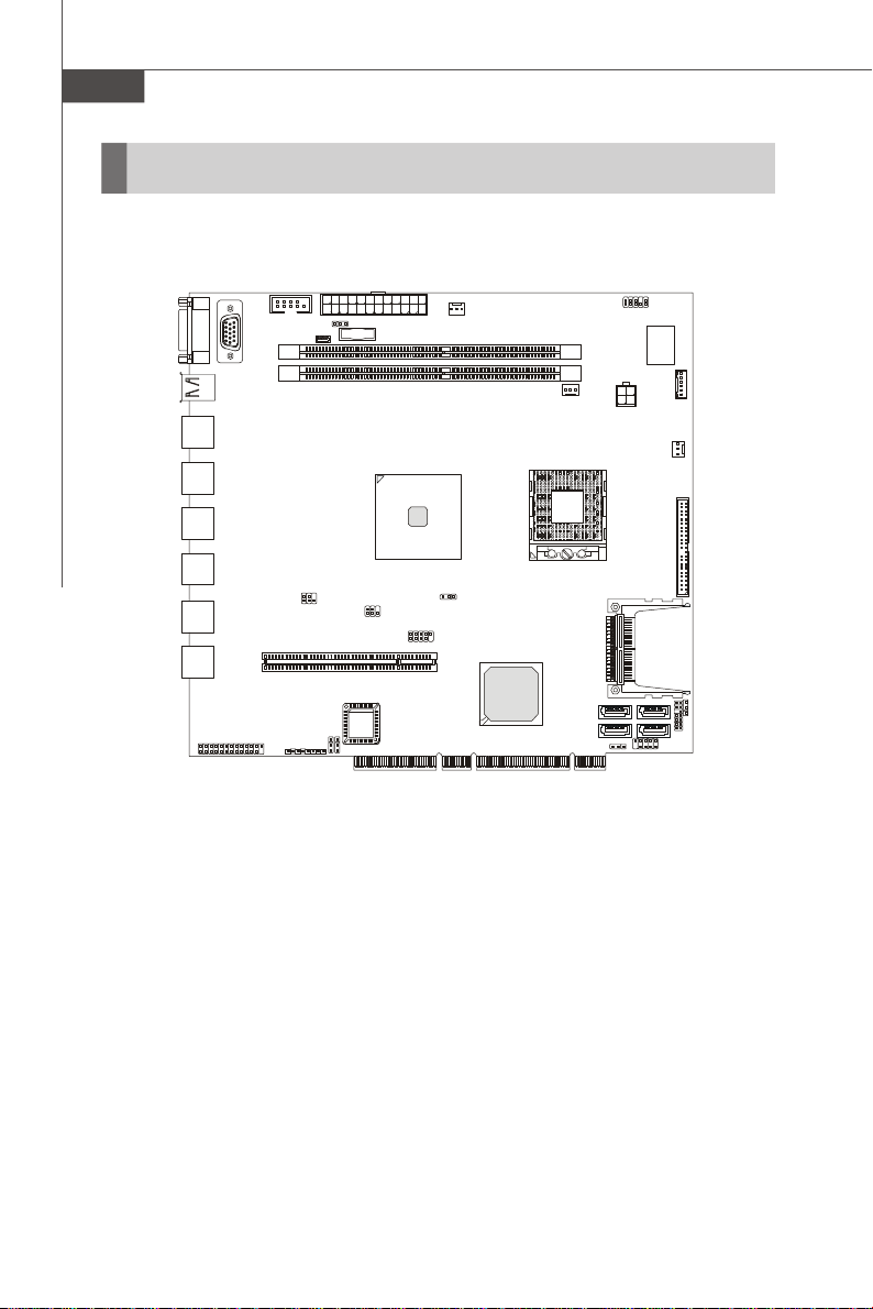
Mainboard Layout
COM1
JLAN0
JLAN1
JLAN2
JLAN3
JLAN4
JLAN5
JUSB0
LAN_LED
COM2
JVGA0
PCI0
CLR_CMOS0
JLCD1
DIMM1
DIMM0
JP1
ATX1
BATT
+
J3
JTV0
J_LAN1
J5
AUXFAN0
J2
F_USB2
PCIE X4 & PCI Bus on Edge
MS-9641 (v2.X) Micro-ATX Mainboard
Intel
SYSFAN1
SATA4
SATA2
JCF_SEL
CF0
W83627EHG
JPW0
J0
Winbond
IDEB0
SATA3
SATA1
JFP1
SM_BUS
JLPC1
JCFV_SEL
1-4
Page 13

Hardware Setup
Chapter 2
Hardware Setup
This chapter provides you with the information about
hardware setup procedures. While doing the installation,
be careful in holding the components and follow the
installation procedures. For some components, if you
install in the wrong orientation, the components will not
work properly.
Use a grounded wrist strap before handling computer
components. Static electricity may damage the
components.
2-1
Page 14
MS-9641 Mainboard
BIOS
Quick Components Guide
Front Panel,
p.2-9
J3,
p.2-17
JTV0,
p.2-15
PCI 0,
p.2-26
LAN_LED,
p.2-17
JLCD1,
p.2-16
COM2,
p.2-15
JP1, p.2-17
CLR_CMOS0,
p.2-24
ATX1, p.2-8
J5, p.2-25
AUXFAN0,
p.2-13
F_USB2,
p.2-14
J2
p.2-25
Golden Finger,
p.2-26
SYSFAN1,
p.2-13
J0, p.2-16
JFP1,
p.2-13
JCF_SEL,
p.2-25
SM_BUS,
p.2-15
DIMM0/1,
p.2-6
JPW0,
p.2-8
CPUFAN0,
p.2-13
CPU,
p.2-3
IDEB0,
p.2-11
CF0, p.2-11
JLPC1,
p.2-16
JCFV_SEL,
p.2-25
SATA1~4,
p.2-12
2-2
Page 15

Hardware Setup
CPU (Central Processing Unit)
The mainboard supports Intel® Core Duo/Core Solo processor in the 478 pin
package. The mainboard uses a CPU socket called mPGA478 for easy CPU installation.
When you are installing the CPU, make sure the CPU has a heat sink and a
cooling fan attached on the top to prevent overheating.
Important
1. Overheating will seriously damage the CPU and system. Always make
sure the cooling fan can work properly to protect the CPU from overheating.
2. Make sure that you apply an even layer of heat sink paste (or thermal tape)
between the CPU and the heatsink to enhance heat dissipation.
3. While replacing the CPU, always turn off the power supply or unplug the
power supply’s power cord from the grounded outlet first to ensure the
safety of CPU.
2-3
Page 16
MS-9641 Mainboard
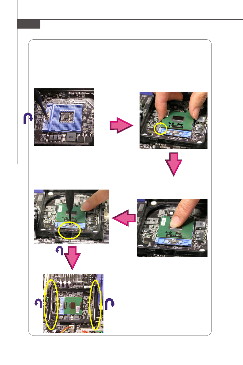
CPU & Cooler Set Installation
1. Loose the screw on the CPU socket with a tank screwdriver in clockwise
direction.
2. Place the CPU on top of the socket. Make sure to align the gold arrow on the
CPU with the arrow key on the socket.
4. On the front end of the CPU socket is a
locking mechanism designed into the
form of a screw. Make sure that you
actuate or deactuate this mechanism
with a screwdriver before and after
installing the CPU.
3. Push the CPU down until its
pins securely fit into the
socket.
2-4
5. Lift up the levers on both sides.
Page 17
Hardware Setup
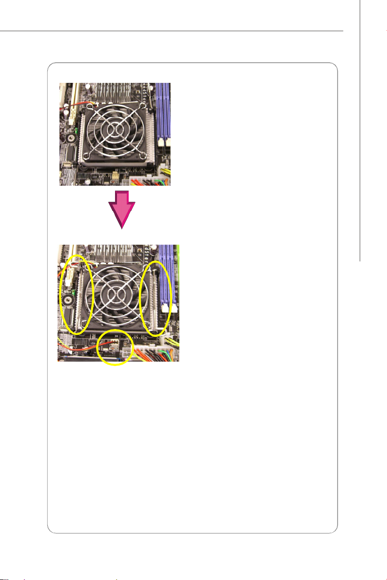
5. Mount the cooler set (fan & heatsink
bundled) on top of the CPU and fit it
into the retention mechanism.
6. Secure the levers to lock the cooler
set.
7. Connect the fan power cable from
the mounted fan to the 3-pin fan
power connector on the board.
2-5
Page 18
MS-9641 Mainboard
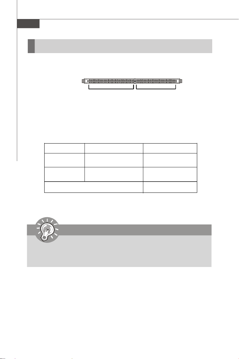
Memory
These DIMM slots are intended for system memory modules.
DDR2
240-pin, 1.8V
64x2=128 pin 56x2=112 pin
Memory Population Rules
Slot Memory Module Total Memory
DIMM 0
(Bank 0 & 1) S/D 128MB~2GB
DIMM 1
(Bank 2 & 3) S/D 128MB~2GB
Maximum System Memory Supported 128MB~4GB
S: Single Side D: Double Side
Important
-Make sure that you install memory modules of the same type and density.
-To enable successful system boot-up, always insert the memory modules
into the DIMM0 first.
2-6
Page 19
Hardware Setup
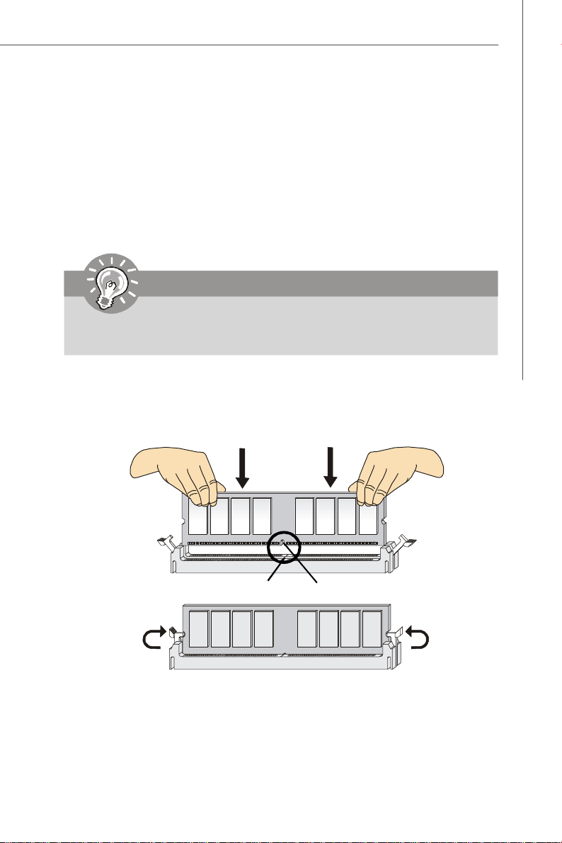
Installing Memory Modules
1. Locate the DIMM slots on the mainboard. Flip open the retaining clip at each side
of the DIMM slot.
2. Align the notch on the DIMM with the key on the slot. Insert the DIMM vertically into
the DIMM slot. Then push it in until the golden finger on the DIMM is deeply inserted
in the DIMM slot. The retaining clip at each side of the DIMM slot will automatically
close if the DIMM is properly seated.
Important
You can barely see the golden finger if the DIMM is properly inserted in the
DIMM slot.
3. Manually check if the DIMM has been locked in place by the retaining clips at the
sides.
4. Follow the same procedures to install more DIMMs if necessary.
Volt
Notch
2-7
Page 20

MS-9641 Mainboard
Power Supply
ATX 24-Pin Power Connector: ATX1
This connector allows you to connect an ATX 24-pin power supply.
To connect the ATX 24-pin power supply, make sure the plug of the
power supply is inserted in the proper orientation and the pins are
aligned. Then push down the power supply firmly into the connector.
You may use the 20-pin ATX power supply as you like. If you’d like
to use the 20-pin ATX power supply, please plug your power supply along with pin 1 & pin 13 (refer to the image at the right hand).
There is also a foolproof design on pin 11, 12, 23 & 24 to avoid
wrong installation.
Pin Definition
PIN SIGNAL
1 +3.3V
2 +3.3V
ATX1
24
12
13
1
3 GND
4 +5V
5 GND
6 +5V
7 GND
8 PWR OK
9 5VSB
10 +12V
11 +12V
12 VCC3
pin 13
pin 12
PIN SIGNAL
13 +3.3V
14 -12V
15 GND
16 PS-ON#
17 GND
18 GND
19 GND
20 Res
21 +5V
22 +5V
23 +5V
24 GND
ATX 12V Power Connector: JPW0
This 12V power connector is used to provide power to the CPU.
JPW1 Pin Definition
3
1
4
2
JPW0
PIN SIGNAL
1 GND
2 GND
3 12V
4 12V
Important
1. Make sure that all the connectors are connected to proper ATX power supplies to ensure stable operation of the mainboard.
2. Power supply of 350 watts (and above) is highly recommended for system
stability.
3. ATX 12V power connection should be greater than 18A.
2-8
Page 21

Front Panel
LAN Bypass Disable
Hardware Setup
WAN
LAN
WAN
LAN
or
WAN
LAN Bypass Enable
Serial Port Connector
The serial port is a 16550A high speed communications port that sends/ receives 16
bytes FIFOs. You can attach a serial mouse or other serial devices directly to the
connector.
USB Connectors
The Universal Serial Bus root is for USB devices such as keyboard, mouse, or other
USB-compatible devices.
LAN
WAN
LAN
2-9
Page 22

MS-9641 Mainboard
LAN (RJ-45) Jack
The standard RJ-45 jack is for connection to single Local Area Network (LAN). You
can connect a network cable to it.
Link IndicatorActivity Indicator
LED Color LED State Condition
Off LAN link is not established.
Left Orange On (steady state) LAN link is established.
On (blinking) The computer is communicating with another computer on the LAN.
Green Off 10 Mbit/sec data rate is selected.
Right On 100 Mbit/sec data rate is selected.
Orange On 1000 Mbit/sec data rate is selected.
2-10
Page 23

Hardware Setup
Connectors
Hard Disk Connector: IDEB0
The mainboard provides a one-channel Ultra ATA 100 bus Master IDE controller that
supports PIO mode 0~4, Bus Master, and Ultra DMA 66/100 function. You can connect hard disk drives, CD-ROM drives and other IDE devices.
IDEB0
IDE UDMA Controller RAID ATAPI
1 66/100 Intel ICH7/ICH7R N/A Yes
IDEB0 (Primary IDE Connector)
IDE1 can connect a Master and a Slave drive. You must configure the second
hard drive to Slave mode by setting the jumper accordingly.
IDE1 Definition
Important
If you install two hard disks on cable, you must configure the second drive to
Slave mode by setting its jumper. Refer to the hard disk documentation
supplied by hard disk vendors for jumper setting instructions.
Compact Flash Card Slot: CF0
This is the slot for Type II Compact Flash (CF) Card.
CF0
2-11
Page 24

MS-9641 Mainboard
Serial ATAII Connectors: SATA1~SATA4
SATA1~SATA4 are high-speed Serial ATA interface ports. Each supports serial ATA
data rates of 3Gb/s. Both connectors are fully compliant with Serial ATA 2.0
specifications. Each Serial ATA connector can connect to 1 hard disk device.
SATA3SATA4
SATA2 SATA1
Important
Please do not fold the SATA accessory cable into 90-degree angle. Otherwise,
data loss may occur during transmission.
2-12
Page 25

Hardware Setup
Fan Power Connectors: CPUFAN0, SYSFAN1, AUXFAN0
The fan power connectors support system cooling fan with +12V. When connecting
the wire to the connectors, always note that the red wire is the positive and should
be connected to the +12V, the black wire is Ground and should be connected to GND.
If the mainboard has a System Hardware Monitor chipset on-board, you must use a
specially designed fan with speed sensor to take advantage of the CPU fan control.
SENSOR
+12V
GND
CPUFAN0
+1 2V
SE NS OR
GND
SYSFAN1
SENSOR
GND
+12V
AUXFAN0
Important
Please refer to the recommended CPU fans at Intel® official website or
consult the vendors for proper CPU cooling fan.
Front Panel Connectors: JFP1
The mainboard provides two front panel connectors for electrical connection to the
front panel switches and LEDs. The JFP1 is compliant with Intel® Front Panel I/O
Connectivity Design Guide.
JFP1
PIN SIGNAL DESCRIPTION
1 HD_LED + Hard disk LED +
2 FP PWR/SLP Power LED +
3 HD_LED - Hard disk active LED
4 FP PWR/SLP Suspend LED +
5 RST_SW - Reset Switch 6 PWR_SW + Power Switch +
7 RST_SW + Reset Switch +
8 PWR_SW - Power Switch 9 RSVD_DNU Reserved.
Reset
HDD
Switch
LED
-
+
-
+
-
+
Power/
Suspend
LED
1
2
9
10
Power
Switch
JFP1 Pin Definition
2-13
Page 26

MS-9641 Mainboard
Front USB Connector: F_USB2
The mainboard provides one USB 2.0 pinheader (optional USB 2.0 bracket available)
that are compliant with Intel® I/O Connectivity Design Guide. USB 2.0 technology
increases data transfer rate up to a maximum throughput of 480Mbps, which is 40
times faster than USB 1.1, and is ideal for connecting high-speed USB interface
peripherals such as USB HDD, digital cameras, MP3 players, printers, mo-
dems and the like.
Pin Definition
PIN SIGNAL PIN SIGNAL
F_USB2
2
1
10
9
1 VCC 2 VCC
3 USB0- 4 USB15 USB0+ 6 USB1+
7 GND 8 GND
9 Key (no pin) 10 USBOC
USB 2.0 Bracket
(Optional)
Important
Note that the pins of VCC and GND must be connected correctly to avoid
possible damage.
2-14
Page 27

Hardware Setup
SMBus Connector: SM_BUS
The mainboard provides one I2C (also known as I2C) Bus connector for users to
connect System Management Bus (SMBus) interface.
SM_BUS
6
1
Pin Definition
PIN SIGNAL
1 GND
2 VCC5V
3 SMBus_Clock
4 SMBus_Data
5 +12V
6 Power Button
TV-Out Connector: JTV0
The mainboard provides a TV-Out connector.
Pin Definition
Pin Description Pin Description
1 TVGND 2 LCVBS
3 LY 4 TVGND
5 LC 6 Key (no pin )
2
1
JTV0
5
Serial Port Connector: COM 2
This connector is a 16550A high speed communications port that sends/receives 16
bytes FIFOs. You can attach a serial device to it.
2 10
1 9
COM2
Pin Definition
PIN SIGNAL DESCRIPTION
1 DCD Data Carry Detect
2 SIN Serial In or Receive Data
3 SOUT Serial Out or Transmit Data
4 DTR Data Terminal Ready
5 GND Ground
6 DSR Data Set Ready
7 RTS Request To Send
8 CTS Clear To Send
9 RI Ring Indicate
2-15
Page 28

MS-9641 Mainboard
LCD Module Connector: JLCD1
This connector is used to connect TTL UART LCD Module.
Pin Definition
JLCD1
1
PIN SIGNAL
1 +5V
2 SINB
3 GND
4 SOUTB
Keyboard/Mouse Connector: J0
This connector is used to connect a mouse/keyboard.
Pin Definition
PIN SIGNAL
J0
19
210
1 +5V
2 +5V
3 KEY
4 NC
5 GND
6 GND
7 Mouse_CLK
8 Keyboard_CLK
9 Mouse_Data
10 Keyboard_Data
FWH/LPC Debugging connector: JLPC1
This connector is for internal debugging only.
JLPC1
1314
2 1
2-16
PIN SIGNAL PIN SIGNAL
1 CLK 2 Key (no pin)
3 RST 4 VCC3
5 LPC_AD0 6 ID
7 LPC_AD1 8 VCC5
9 LPC_AD2 10 Key (no pin)
11 LPC_AD3 12 GND
13 LPC_FRAME# 14 GND
Pin Definition
Page 29

Hardware Setup
LAN_LED
2
1
LAN_LED
Pin Definition
Pin Description Pin Description
1 LAN2_LED_ACT 2 LAN2_LED
3 LAN2_LED_LINK 10/100 4 LAN2_LED_LINK 1000_P
5 LAN1_LED_ACT 6 LAN1_LED
7 LAN1_LED_LINK 10/100 8 LAN1_LED_LINK 1000_P
9 LAN4_LED_ACT 10 LAN4_LED
11 LAN4_LED_LINK 10/100 12 LAN4_LED_LINK 1000_P
13 LAN3_LED_ACT 14 LAN3_LED
15 LAN3_LED_LINK 10/100 16 LAN3_LED_LINK 1000_P
17 LAN5_LED_ACT 18 LAN5_LED
19 LAN5_LED_LINK 10/100 20 LAN5_LED_LINK 1000_P
21 LAN6_LED_ACT 22 LAN6_LED
23 LAN6_LED_LINK 10/100 24 LAN6_LED_LINK 1000_P
25 KEY 26 NC
LAN ByPass LED Pinheader: J3
J3
2
5
1
26
25
Pin Definition
Pin Description Pin Description
1 VCC3 2 LAN Bypass 1 LED
3 VCC3 4 LAN Bypass 2 LED
5 NC
CPLD Data Reflash Pinheader:JP1
Pin Description Pin Description
1
JP1
8
1 VCC 2 TDD
3 TDI 4 IspEN
5 TRST 6 TMS
7 GND 8 TCK
Pin Definition
2-17
Page 30

MS-9641 Mainboard
LAN Bypass Definition
Bypass setting in BIOS
Power
BIOS Bypass Se ing ! Bypass Behavior
status
On Bypass mode a er power on !
Bypass mode a er power o" !!
O" !
(All segment or by each segment are controllable)
Pass Through Behavior: A
Disable A
Enable B
Disable A
Enable B
Bypass Behavior: B
2-18
Page 31

LAN5, LAN6 have no by pass function.
numbered 1 thru 4.
Programming Guide
LPC I/O address : 5E
SMBus address: 0X00 (optional)
1.Power ON State Bypass Control Status Register
Set/Read bypass mode
Default Value: 0x00 (Base on Customer Demand)
Hardware Setup
Bit Definition
Bit Field Name Value
03:00 Segment
4 Path sel
5 reserved
6 reserved
7 GPIO sel
Power ON State Bypass Control Status Register
1 to 4
Segment control bit. Each bit corresponds to a specific segment
:
Write
1: Force Bypass
0: Force Pass Through
:
Read
1: Bypass Mode
0: Pass Through Mode
0:LPC Control LAN
1:GPIO Control LAN
0:GPIO38 and GPIO39 :control LAN1,LAN2
1:GPIO38 controls LAN1,GPIO39 controls LAN2
2-19
Page 32

MS-9641 Mainboard
Signal Action
Segment Signal Name Description Type Bypass Pass Through
Segment 1
Segment 2
Segment 3
Segment 4
RELAY_SET1# Enable LAN1 bypass Output 1 0
RESET_RESET1# Enable LAN1 bypass Output 0 1
BYPASS1_LED# Enable LAN1 bypass LED Output 1 0
RELAY_SET2# Enable LAN2 bypass Output 1 0
RESET_RESET2# Enable LAN2 bypass Output 0 1
BYPASS2_LED# Enable LAN2 bypass LED Output 1 0
RELAY_SET3# Enable LAN3 bypass Output 1 0
RESET_RESET3# Enable LAN3 bypass Output 0 1
BYPASS3_LED# Enable LAN3 bypass LED Output 1 0
RELAY_SET4# Enable LAN4 bypass Output 1 0
RESET_RESET4# Enable LAN4 bypass Output 0 1
BYPASS4_LED# Enable LAN4 bypass LED Output 1 0
2.WDTO# to Bypass Control Mask Register
Mask WDTO# input for bypass mode
When WDTO# pin inputs 0, watchdog timeout occurs. This register sets watchdog
timeout behavior for Segment 1~4.
WDTO# - Input from Super I/O WDTO#
Default Value: 0x00
7 6 5 4 3 2 1 0
X R/W R/W R/W R/W R/W R/W R/W
GPIO sel SMI Reset Path sel Segment 4 Segment 3 Segment 2 Segment 1
WDTO# Input
0 1 No Change
0 0 Bypass
1 X No Change
WDTO# to Bypass Control Mask Register
Segment bit (bit 0~4)
Mode
Bit Definition
Bit Field Name Value
3:0 Segment
4 Path sel 0:LPC Control LAN
5 reserved
6 reserved
7 GPIO sel 0:GPIO38 and GPIO39 :control LAN1,LAN2
WDTO# to Bypass Control Mask Register
1 to 4
WDTO# to Bypass Control Segment bit mask. Each bit
corresponds to a specific segment numbered 1 thru 4.
Read/Write:
1: When WDTO# active, then set Segment Bypass Mode
0: When WDTO# active, no action
1:GPIO Control LAN
(1→ BYPASS 0→Pass Through)
1:GPIO38 control LAN1,GPIO39 control LAN2 :
(GPIO38:1→ BYPASS 0→Pass Through
GPIO39:1→ BYPASS 0→Pass Through)
2-20
Page 33

Hardware Setup
3.Power Off to Bypass Control Register
Enable/Disable Low Voltage Detect (3.08VDETECT) input for bypass mode
When 3.08VDETECT pin input 0, then low voltage detected. This register sets
power off behavior for Segment 1~5
3.08VDETECT - Input from Voltage Supervisor. When +12V input under +11V, then
this signal will change to 0.
2-21
Page 34

MS-9641 Mainboard
Method 1: GPIO control Bypass (GPIO Mode)
ByPass Normal
SB GPIO38(Relay1) High Low
SB GPIO39(Relay2) High Low
Note: GPIO Mode has two configuration. One is GPIO38,39 controlling together; the
other is GPIO38,39 controlling individually.
Method 2: LPC Control Bypass (LPC Mode)
LPC I/O Address: 5E ByPass Normal
Bit[0..3] corresponds to LAN [1..4] High Low
Note: bit 0 = 1, change LAN 1, 2 to bypass,
bit 0 = 0, change LAN 1, 2 to normal (power on status)
bit 1 = 1, change LAN 3, 4 to bypass,
bit 1 = 0, change LAN 3, 4 to normal (power on status)
bit 2 = 1, change LAN 1, 2 to bypass,
bit 2 = 0, change LAN 1, 2 to normal (power off status)
bit 3 = 1, change LAN 3, 4 to bypass,
bit 3 = 0, change LAN 3, 4 to normal (power off status)
Sample code (Method 1: GPIO Mode)
Set GPIO38, 39 to Control LAN GPIO38,39 control together
mov al,10h ;GPIO38,39 control By pass (BIT4=1,BIT 7=0)
mov dx,005eh ; if GPIO38,39 control dividually, set BIT 4=1, BIT7=1)
out dx,al ; Choose GPIO Mode and GPIO 38 ,39 together control configration
mov dx,480h + 30h ;Select SB GPIO
in eax,dx
or eax,0C0h ;Select GPIO 38,39
out dx,eax
mov dx,480h + 34h ;Control IN/OUT
in eax,dx
and eax,Not 0C0h
out dx,eax
mov dx,480h + 38h
in al,dx
and al,not 11000000b ;Enable GPIO 38,39
or al,11000000b
out dx,al
2-22
Page 35

Sample Code (Method 2: LPC Mode)
Control LPC LAN
mov al,0fh ;Select LPC Mode (bit 4 =1)
mov dx,005eh
out dx,al
Note: bit 0 = 1, change LAN 1, 2 to bypass,
bit 0 = 0, change LAN 1, 2 to normal (power on status)
bit 1 = 1, change LAN 3, 4 to bypass,
bit 1 = 0, change LAN 3, 4 to normal (power on status)
bit 2 = 1, change LAN 1, 2 to bypass,
bit 2 = 0, change LAN 1, 2 to normal (power off status)
bit 3 = 1, change LAN 3, 4 to bypass,
bit 3 = 0, change LAN 3, 4 to normal (power off status)
Watch Dog function setup sample code
mov dx, 4Eh ;Send "87" twice to IO port 4Eh
mov al, 87h ;to unlock SIO.
out dx, al
out dx, al
mov dx, 4Eh
mov al, 2Dh
out dx, al
mov dx, 4Fh
in al, dx
and al, 11111110b ;Set PIN77 to WDTO#
out dx, al
mov dx, 4Eh ;Choose LDN8
mov al, 07h
out dx, al
mov dx, 4Fh
mov al, 08h
out dx, al
mov dx, 4Eh ;Set to enable
mov al, 30h
out dx, al
mov dx, 4Fh
mov al, 01h
out dx, al
mov dx, 4Eh ;Enable WDTO# and set to KBRST#
mov al, 0F7h
out dx, al
mov dx, 4Fh
in al, dx
and al, 0F7h ;CR 0F7h bit4 --> 0 (clear event)
out dx, al
.. ;CR 0F6h bit0--7 : Set counter time
.. ;CR 0F5h bit1 --> 1 (Enable WDTO# and KBRST#)
.. bit3 ---> 0 (Second mode), 1 (Minute mode)
mov dx, 4Eh ;Exit SIO access and lock it up.
mov al, 0AAh
out dx, al
Hardware Setup
2-23
Page 36

MS-9641 Mainboard
Jumpers
Clear CMOS Jumper: CLR_CMOS0
There is a CMOS RAM onboard that has a power supply from external battery to keep
the data of system configuration. With the CMOS RAM, the system can automatically
boot OS every time it is turned on. If you want to clear the system configuration, set
the CLR_CMOS0 (Clear CMOS Jumper ) to clear data.
1
CLR_CMOS0
1
Clear Data
3
1
Keep Data
3
Important
You can clear CMOS by shorting 1-2 pin while the system is off. Then return
to 2-3 pin position. Avoid clearing the CMOS while the system is on; it will
damage the mainboard.
2-24
Page 37

Hardware Setup
GMCH Voltage Jumper: J2
This jumper is used to adjust the voltage of the Intel 945GME GMCH (Graphics and
Memory Controller Hub) as a way to enhance graphics performance.
1
J2
1.05V 1.5V
AT/ATX Power Select Jumper: J5
1
J5
AT
JCF_SEL & JCFV_SEL
1
JCF_SEL
VCC3 VCC5
3
3
1
1
3
ATX
3
1
13
1
3
13
3
1
JCFV_SEL
1
Master
1
Slave
2-25
Page 38

MS-9641 Mainboard
Slot
Golden Finger
TOP View
B94
BOTTOM View
A94
PCI (Peripheral Component Interconnect) Slot
The PCI slots support LAN cards, SCSI cards, USB cards, and other add-on cards
that comply with PCI specifications. At 32 bits and 33 MHz, it yields a throughput rate
of 133 MBps.
32-bit PCI Slot
B1
A1
Important
When adding or removing expansion cards, make sure that you unplug the
power supply first. Meanwhile, read the documentation for the expansion card
to configure any necessary hardware or software settings for the expansion
card, such as jumpers, switches or BIOS configuration.
2-26
Page 39

Chapter 3
BIOS Setup
This chapter provides information on the BIOS Setup
program and allows you to configure the system for
optimum use.
You may need to run the Setup program when:
² An error message appears on the screen during the
system booting up, and requests you to run SETUP.
² You want to change the default settings for cus-
tomized features.
BIOS Setup
3-1
Page 40

MS-9641 Mainboard
Entering Setup
Power on the computer and the system will start POST (Power On Self Test) process.
When the message below appears on the screen, press <F1> key to enter Setup.
Press F1 to enter SETUP
If the message disappears before you respond and you still wish to enter Setup,
restart the system by turning it OFF and On or pressing the RESET button. You may
also restart the system by simultaneously pressing <Ctrl>, <Alt>, and <Delete> keys.
Important
1. The items under each BIOS category described in this chapter are under
continuous update for better system performance. Therefore, the description may be slightly different from the latest BIOS and should be held for
reference only.
2.Upon boot-up, the 1st line appearing after the memory count is the BIOS
version. It is usually in the format:
3-2
P9641IMS V2.0 031908 where:
1st digit refers to BIOS maker as A = AMI, W = AWARD, and P =
PHOENIX.
2nd - 5th digit refers to the model number.
6th digit refers to the chipset as I = Intel, N = nVidia, and V = VIA.
7th - 8th digit refers to the customer as MS = all standard customers.
V2.0 refers to the BIOS version.
031908 refers to the date this BIOS was released.
Page 41

BIOS Setup
Control Keys
<↑> Move to the previous item
<↓> Move to the next item
<←> Move to the item in the left hand
< →> Move to the item in the right hand
<Enter> Select the item
<Esc> Jumps to the Exit menu or returns to the main menu from a
submenu
<+/PU> Increase the numeric value or make changes
<-/PD> Decrease the numeric value or make changes
<F6> Load Fail-Safe Defaults
<F7> Load Optimized Defaults
<F10> Save all the CMOS changes and exit
Getting Help
After entering the Setup menu, the first menu you will see is the Main Menu.
Main Menu
The main menu lists the setup functions you can make changes to. You can use the
arrow keys ( ↑↓ ) to select the item. The on-line description of the highlighted setup
function is displayed at the bottom of the screen.
Sub-Menu
If you find a right pointer symbol (as shown in the right view)
appears to the left of certain fields that means a sub-menu
can be launched from this field. A sub-menu contains additional options for a field parameter. You can use arrow keys
( ↑↓ ) to highlight the field and press <Enter> to call up the
sub-menu. Then you can use the control keys to enter values and move from field to
field within a sub-menu. If you want to return to the main menu, just press the <Esc>.
General Help <F1>
The BIOS setup program provides a General Help screen. You can call up this screen
from any menu by simply pressing <F1>. The Help screen lists the appropriate keys
to use and the possible selections for the highlighted item. Press <Esc> to exit the
Help screen.
3-3
Page 42

MS-9641 Mainboard
The Menu Bar
Main
Use this menu for basic system configurations, such as time, date etc.
Advanced
Use this menu to set up the items of special enhanced features available on your
system’s chipset.
Boot
Use this menu to specify the priority of boot devices.
Security
Use this menu to set Supervisor and User Passwords.
System
This entry shows your system summary.
PC Health
This entry monitors your hardware health status.
Exit
This menu allows you to load the BIOS default values or factory default settings into
the BIOS and exit the BIOS setup utility with or without saving changes.
3-4
Page 43

Main
Date (mm:dd:yy)
The date format is <Day>, <Month> <Date> <Year>.
Time (hh:mm:ss)
The time format is <Hour> <Minute> <Second>.
BIOS Setup
IDE Channel 0 Master/Slave, IDE Channel 1 Master/Slave
IDE Channel 0 Master Press PgUp/<+> or PgDn/<-> to select [Manual],
[None] or [Auto] type. Note that the specifications
3-5
Page 44

MS-9641 Mainboard
of your drive must match with the drive table. The
hard disk will not work properly if you enter improper information for this category. If your hard
disk drive type is not matched or listed, you can
use [Manual] to define your own drive type
Access Mode The settings are [CHS], [LBA], [Large], [Auto].
Capacity The formatted size of the storage device.
Cylinder Number of cylinders.
Head Number of heads.
Precomp Write precompensation.
Landing Zone Cylinder location of the landing zone.
Sector Number of sectors.
Video
Select the type of primary video subsystem in your computer. The BIOS usually
detects the correct video type automatically. The BIOS supports a secondary video
subsystem, but you do not select it in Setup.
[EGA/VGA] Enhanced Graphics Adapter/Video Graphics Array. For EGA,
VGA, SEGA, SVGA or PGA monitor adapters.
[CGA 40] Color Graphics Adapter, power up in 40 column mode.
[CGA 80] Color Graphics Adapter, power up in 80 column mode.
[MONO] Monochrome adapter, includes high resolution monochrome
adapters
Base/Extended/Total Memory
The three items show the memory status of the system. (Read-only)
manually.
3-6
Page 45

Advanced
Advanced BIOS Features
BIOS Setup
Virus Warning
The item is to set the Virus Warning feature for IDE Hard Disk boot sector
protection. If the function is enabled and any attempt to write data into this area
is made, BIOS will display a warning message on screen and beep.
CPU L3 Cache
Level 3 cache is the extra cache built into motherboards between the micropro-
3-7
Page 46

MS-9641 Mainboard
cessor and the main memory. Located away from the CPU, the L3 cache is
slower than the L1 & L2 caches. This setting allows you to turn on or off the L3
cache.
Quick Power On Self Test
Select [Enabled] to reduce the amount of time required to run the power-on selftest (POST). A quick POST skips certain steps. We recommend that you normally disable quick POST. Better to find a problem during POST than lose data
during your work.
APIC Mode
This field is used to enable or disable the APIC (Advanced Programmable Interrupt Controller). Due to compliance with PC2001 design guide, the system is
able to run in APIC mode. Enabling APIC mode will expand available IRQ resources for the system.
MPS Version Control For OS
This field allows you to select which MPS (Multi-Processor Specification) version to be used for the operating system. You need to select the MPS version
supported by your operating system. To find out which version to use, consult
the vendor of your operating system.
Console Redirection
Console Redirection operates in host systems that do not have a monitor and
keyboard attached. This setting enables/disables the operation of console
redirection. When set to [Enabled], BIOS redirects and sends all contents that
should be displayed on the screen to the serial COM port for display on the
terminal screen. Besides, all data received from the serial port is interpreted as
keystrokes from a local keyboard.
Flow Control
This feature allows you to enable flow control.
Baud Rate
This setting specifies the transfer rate (bits per second) of Console Redirection.
Agent Connect via
To operate the system’s console redirection, you need a terminal supporting
ANSI terminal protocol and a RS-232 null modem cable connected between the
host system and terminal(s). The field is a read-only field, which is used to
indicate the type of device connected between the host system and terminal
(s). NULL stands for a null modem.
Agent wait time (min)
This setting controls the timeout for terminals’ (console redirection) connection
to the host system.
Agent after boot
This setting determines whether or not to keep terminals’ console redirection
running after the OS has booted.
3-8
Page 47

BIOS Setup
Advanced Chipset Features
DRAM Timing Selectable
Selects whether DRAM timing is controlled by the SPD (Serial Presence Detect)
EEPROM on the DRAM module. Setting to [By SPD] enables DRAM timing to be
determined automatically by BIOS based on the configurations on the SPD.
Selecting [Manual] allows users to configure the following fields manually.
CAS Latency Time
This controls the timing delay (in clock cycles) before SDRAM starts a read
command after receiving it. Smaller clocks increase system performance while
bigger clocks provide more stable system performance.
DRAM RAS# to CAS# Delay
This field allows you to set the number of cycles for a timing delay between the
CAS and RAS strobe signals, used when DRAM is written to, read from or
refreshed. Fast speed offers faster performance while slow speed offers
more stable performance.
DRAM RAS# Precharge
This item controls the number of cycles for Row Address Strobe (RAS) to be
allowed to precharge. If insufficient time is allowed for the RAS to accumulate
its charge before DRAM refresh, refresh may be incomplete and DRAM may fail
to retain data. This item applies only when synchronous DRAM is installed in the
system.
Precharge Delay (tRAS)
The field specifies the idle cycles before precharging an idle bank.
System Memory Frequency
Use this item to configure the clock frequency of the installed DRAMs.
3-9
Page 48

MS-9641 Mainboard
**VGA Setting**
The following items allow you to configure the VGA settings of the system.
PEG/Onchip VGA Control
This setting allows you to select whether to use the onchip graphics processor
or the PCI Express card.
When set to [Onchip VGA], the motherboard boots up using the onboard graphics processor, even when a PCI Express graphics card is installed.
When set to [PEG Port], the motherboard boots up using the PCI Express graphics card, if one is installed. Otherwise, it defaults to the onboard graphics
processor.
When set to [Auto], the BIOS checks to see if a PCI Express graphics card is
installed. If it detects that a PCI Express graphics card is present, the motherboard
boots up using that card. Otherwise, it defaults to the onboard graphics
processor.
On-Chip Frame Buffer Size
The field specifies the size of system memory allocated for video memory.
Boot Display
Use the field to select the type of device you want to use as the display(s) of
the system.
TV Format
Select the TV format if you have connected a TV to the system.
3-10
Page 49

Integrated Peripherals
OnChip IDE Device
BIOS Setup
IDE HDD Block Mode
Block mode is also called block transfer, multiple commands, or multiple
sector read/write. If your IDE hard drive supports block mode (most new
drives do), select [Enabled] for automatic detection of the optimal number of
block read/writes per sector the drive can support.
IDE DMA Transfer Access
Setting to [Enabled] will open DMA bus master and execute DMA action in
DOS, which will make the data transferring faster.
On-Chip Primary/Secondary PCI IDE
The chipset contains a PCI IDE interface with support for two IDE channels.
Select [Enabled] to activate the first and/or second IDE interface. Select
3-11
Page 50

MS-9641 Mainboard
[Disabled] to deactivate an interface, if you install a primary and/or secondary add-in IDE interface.
IDE Primary/Secondary Master/Slave PIO
The IDE PIO (Programmed Input/Output) fields let you set a PIO mode for the
IDE devices that the onboard IDE interface supports. Modes 0 through 4
provide successively increased performance. In [Auto] mode, the system
automatically determines the best mode for each device.
IDE Primary/Secondary Master/Slave UDMA
Ultra DMA 33/66/100/133 implementation is possible only if your IDE hard
drive supports it and the operating environment includes a DMA driver
(Windows ME, XP or a third-party IDE bus master driver). If your hard drive
and your system software both support Ultra DMA/33, Ultra DMA/66, Ultra
DMA/100 and Ultra DMA/133, select [Auto] to enable BIOS support.
*** On-Chip Serial ATA Setting ***
SATA Mode
This setting specifies the SATA controller operation mode.
On-Chip Serial ATAA
This setting specifies the function of the on-chip SATA controller.
[Disabled] Disable SATA controller
[Auto] Automatically determined by BIOS
[Enhanced Mode] Enable both SATA and PATA, max. 6 IDE
[SATA Only] SATA operates in legacy mode
drives supported
3-12
SATA Port Speed Settings
This setting controls the speed of the SATA port.
PATA IDE Mode / SATA Port
These settings specify the modes of the PATA & SATA ports.
Page 51

BIOS Setup
Onboard Device
Power On LAN ByPass, Power Off LAN ByPass
LAN Bypass feature removes a single point of failure so that essential
business communication can continue while a network failure is diagnosed
and resolved. In the event of a power, hardware or software failure, Hardware Bypass will automatically activate, allowing network traffic to continue.
Traffic between the LAN and WAN is allowed without interruption.
Power on LAN Bypass selects the [LPC] or [GPIO] bypass mode for power
on. Power off LAN Bypass selects the [LPC] bypass mode for power off.
Planar Ethernet #01/ #02/ #03/ #04/ #05/ #06
These settings disable/enable the onboard Ethernet controller.
PXE Boot
The Preboot Execution Environment (PXE) is an environment to boot computers using a network interface card independently of available data storage
devices (like hard disks) or installed operating systems.
USB Controller, USB 2.0 Controller
This setting is used to enable/disable the onboard USB / USB2.0 controller.
USB Keyboard/Mouse Support
Set to [Enabled] if your need to use a USB-interfaced keyboard/mouse in the
operating system that does not support or have any USB driver installed,
such as DOS and SCO Unix.
3-13
Page 52

MS-9641 Mainboard
Super IO Device
Onboard Serial Port 1 / 2
Select an address and corresponding interrupt for Serial Port 1/2.
UART Mode Select
This setting allows you to specify the operation mode for serial port 2.
[Normal] RS-232C Serial Port
[IrDA] IrDA-compliant Serial Infrared Port
[ASKIR] Amplitude Shift Keyed Infrared Port
3-14
RxD, TxD Active
This setting controls the receiving and transmitting speed of the IR peripheral
in use.
IR Transmission Delay
This setting determines whether the IR transmission rate will be delayed
while converting to receiving mode.
UR2 Duplex Mode
This setting controls the operating mode of IR transmission/reception. Under
[Full] Duplex mode, synchronous, bi-directional transmission/reception is
allowed. Under [Half] Duplex mode, only asynchronous, bi-directional transmission/reception is allowed.
Use IR Pins
Consult your IR peripheral documentation to select the correct setting of the
TxD and RxD signals.
Watch Dog
You can enable the system watch-dog timer, a hardware timer that generates either an NMI or a reset when the software that it monitors does not
respond as expected each time the watch dog polls it.
Page 53

Watch Dog Action
Select the watch-dog timer response.
Watch Dog Timer (Minutes)
Select the watch-dog timer period.
COM Port Select
This setting specifies the serial port operation mode.
Power Management Setup
BIOS Setup
Power Type
This setting shows the power supply type. Read only.
PCI Express PME
This setting specifies whether the system will be awakened by the PCI Express
PME (Power Management Event).
ACPI Function
This item is to activate the ACPI (Advanced Configuration and Power Management Interface) Function. If your operating system is ACPI-aware, such as
Windows 98SE/2000/ME, select [Enabled].
ACPI Suspend Type
This item specifies the power saving modes for ACPI function. If your operating
system supports ACPI, such as Windows 98SE, Windows ME and Windows
2000, you can choose to enter the Standby mode in S1 (POS) or S3 (STR)
fashion through the setting of this field. Options are:
[S1(POS)]The S1 sleep mode is a low power state. In this state,
no system context is lost (CPU or chipset) and hardware maintains all system context.
[S3(STR)]The S3 sleep mode is a lower power state where the
information of system configuration and open appli-
3-15
Page 54

MS-9641 Mainboard
cations/files is saved to main memory that remains
powered while most other hardware components turn
off to save energy. The information stored in memory
will be used to restore the system when a “wake up”
event occurs.
Soft-Off by PWR-BTTNN
This feature allows users to configure the power button function. Settings are:
[Instant-Off] The power button functions as a normal power-on/-off button.
[Delay 4 Sec.]When you press the power button, the computer enters the
Wake-Up by PCI Card
When setting to [Enabled], this setting allows your system to be awakened from
the power saving modes through any event on PCI PME (Power Management
Event).
USB KB Wake-Up from S3
This setting allows you to enter “Any Key” (max. 8 numbers) to wake up the
system from S3 state.
Resume by Alarm
When [Enabled], your can set the date and time at which the RTC (real-time
clock) alarm awakens the system from suspend mode.
Date (of Month) Alarm
When Resume By Alarm is set to [Enabled], the field specifies the month for
Resume By Alarm.
suspend/sleep mode, but if the button is pressed for more
than four seconds, the computer is turned off.
Time (hh:mm:ss) Alarm
You can choose what hour, minute and second the system will boot up.
PWRON After PWR-Fail
This item specifies whether your system will reboot after a power failure or
interrupt occurs. Available settings are:
Boot Up NumLock Status
This setting is to set the Num Lock status when the system is powered on. Setting to
[On] will turn on the Num Lock key when the system is powered on. Setting to [Off]
will allow users to use the arrow keys on the numeric keypad.
Auto Detect PCI Clk
This item is used to auto detect the PCI slots. When set to [Enabled], the system will
[Off] Leaves the computer in the power off state.
[On] Leaves the computer in the power on state.
[Former-sts] Restores the system to the status before power fail-
ure or interrupt occurred.
3-16
Page 55

BIOS Setup
remove (turn off) clocks from empty PCI slots to minimize the electromagnetic interference (EMI).
Spread Spectrum
When the motherboard’s clock generator pulses, the extreme values (spikes) of the
pulses creates EMI (Electromagnetic Interference). The Spread Spectrum function
reduces the EMI generated by modulating the pulses so that the spikes of the pulses
are reduced to flatter curves.
Important
1.If you do not have any EMI problem, leave the setting at [Disabled] for
optimal system stability and performance. But if you are plagued by EMI,
select the value of Spread Spectrum for EMI reduction.
2.The greater the Spread Spectrum value is, the greater the EMI is reduced,
and the system will become less stable. For the most suitable Spread
Spectrum value, please consult your local EMI regulation.
3.Remember to disable Spread Spectrum if you are overclocking because
even a slight jitter can introduce a temporary boost in clock speed which
may just cause your overclocked processor to lock up.
3-17
Page 56

MS-9641 Mainboard
Boot
Removable Device Priority
This setting allows users to set the priority of the removable devices. Refer to the
Item Help on the right pane for instructions.
3-18
Page 57

BIOS Setup
Hard Disk Boot Priority
This setting allows users to set the boot priority of the specified hard disk devices.
Refer to the Item Help on the right pane for instructions.
CD-ROM Boot Priority
This setting allows users to set the boot priority of the specified CD-ROM devices.
Refer to the Item Help on the right pane for instructions.
First / Second / Third Boot Device
The items allow you to set the sequence of boot devices where BIOS attempts to load
the disk operating system.
Boot Other Device
Setting the option to [Enabled] allows the system to try to boot from other device if the
system fails to boot from the first/second/third boot device.
3-19
Page 58

MS-9641 Mainboard
Security
Set Supervisor Password
Supervisor Password controls access to the BIOS Setup utility.
Set User Password
User Password controls access to the system at boot.
Security Option
This specifies the type of BIOS password protection that is implemented. Settings are
described below:
Option Description
[Setup] The password prompt appears only when end users try to run
[System] A password prompt appears every time when the computer is
Setup.
powered on or when end users try to run Setup.
3-20
Page 59

BIOS Setup
System
System Summary
These items show the hardware specifications of your system. Read only.
Halt On
The setting determines whether the system will stop if an error is detected at boot.
When the system stops for the errors preset, it will halt on for 15 seconds and then
automatically resume its operation. Available options are:
[All Errors] The system stops when any error is detected.
[No Errors] The system doesn’t stop for any detected error.
[All, But Keyboard] The system doesn’t stop for a keyboard error.
3-21
Page 60

MS-9641 Mainboard
PC Health
Smart Fan Setting
The sub-menu is used to control fan speeds for optimal system performance.
Smart SYSFan1 / CPUFan1 / SYSFan2 Temperature
Select a temperature setting here, and if the temperature of the CPU/system
climbs up to the selected temperature setting, the system will automatically
increase the speed of the CPU/system fan to cool down the overheated CPU/
system.
3-22
Page 61

BIOS Setup
SYSFan1 / CPUFan1 / SYSFan2 Tolerance Value
You can select a fan tolerance value here for the specific range for the Smart
SYSFan1 / CPUFan1 / SYSFan2 Temperature items. If the current tempera-
tures of the fans reach to the maximum threshold (the temperatures set in the
Smart SYSFan1 / CPUFan1 / SYSFan2 Temperature plus the tolerance
values you set here), the fans will speed up for cooling down. On the contrary
if the current temperatures reach to the minimum threshold (the set temperatures minus the tolerance values), the fans will slow down to keep the temperatures stable.
Current System Temp 1, Current CPU1 Temperature, Current Systemm
Temp 2, SYSFan1 Speed, CPUFan1 Speed, SYSFan2 Speed, Vcore, 12V,
V_1P5_Core, VCC_DDR2, VCC3, VBAT(V), 3VSB(V)
These items display the current status of all of the monitored hardware devices/
components such as CPU voltage, temperatures and all fans’ speeds.
3-23
Page 62

MS-9641 Mainboard
Exit
Load Fail-Safe Defaults
Use this menu to load the default values set by the BIOS vendor for stable system
performance.
Load Optimized Defaults
Use this menu to load the default values set by the mainboard manufacturer specifically for optimal performance of the mainboard.
Save & Exit Setup
Save changes to CMOS and exit setup.
Exit Without Saving
Abandon all changes and exit setup.
3-24
 Loading...