

Page 1

i
English/French/German version
G52-M7053X6
MS-7053 (v1.X) ATX Mainboard
925X Neo
Page 2
ii
Manual Rev: 1.1
Release Date: June 2004
FCC-B Radio Frequency Interference Statement
This equipment has been tested and found to comply with the limits for a class B
digital device, pursuant to part 15 of the FCC rules. These limits are designed to
provide reasonable protection against harmful interference when the equipment is
operated in a commercial environment. This equipment generates, uses and can
radiate radio frequency energy and, if not installed and used in accordance with the
instruction manual, may cause harmful interference to radio communications. Operation
of this equipment in a residential area is likely to cause harmful interference, in which
case the user will be required to correct the interference at his own expense.
Notice 1
The changes or modifications not expressly approved by the party responsible for
compliance could void the user’s authority to operate the equipment.
Notice 2
Shielded interface cables and A.C. power cord, if any, must be used in order to
comply with the emission limits.
VOIR LA NOTICE D’INSTALLATION A VANT DE RACCORDER AU RESEAU.
Micro-Star International
MS-7053
This device complies with Part 15 of the FCC Rules. Operation is subject to the
following two conditions:
(1) this device may not cause harmful interference, and
(2) this device must accept any interference received, including interference that
may cause undesired operation
Page 3

iii
Copyright Notice
The material in this document is the intellectual property of MICRO-STAR
INTERNATIONAL . We take every care in the preparation of this document, but no
guarantee is given as to the correctness of its contents. Our products are under
continual improvement and we reserve the right to make changes without notice.
Trademarks
All trademarks are the properties of their respective owners.
AMD, Athlon™, Athlon™ XP, Thoroughbred™, and Duron™ are registered
trademarks of AMD Corporation.
Intel® and Pentium® are registered trademarks of Intel Corporation.
PS/2 and OS®/2 are registered trademarks of International Business Machines
Corporation.
Microsoft is a registered trademark of Microsoft Corporation. Windows® 98/2000/NT/
XP are registered trademarks of Microsoft Corporation.
NVIDIA, the NVIDIA logo, DualNet, and nForce are registered trademarks or trademarks of NVIDIA Corporation in the United States and/or other countries.
Netware® is a registered trademark of Novell, Inc.
Award® is a registered trademark of Phoenix Technologies Ltd.
AMI® is a registered trademark of American Megatrends Inc.
Kensington and MicroSaver are registered trademarks of the Kensington Technology
Group.
PCMCIA and CardBus are registered trademarks of the Personal Computer Memory
Card International Association.
Revision History
Revision Revision History Date
V1.0 First release for PCB 1.X June 2004
with Intel 925X & Intel ICH6/ICH6R
V1.1 Multi-lingual version June 2004
Page 4

iv
1. Always read the safety instructions carefully.
2. Keep this User’s Manual for future reference.
3. Keep this equipment away from humidity.
4. Lay this equipment on a reliable flat surface before setting it up.
5. The openings on the enclosure are for air convection hence protects the equipment from overheating. Do not cover the openings.
6. Make sure the voltage of the power source and adjust properly 110/220V before connecting the equipment to the power inlet.
7. Place the power cord such a way that people can not step on it. Do not place
anything over the power cord.
8. Always Unplug the Power Cord before inserting any add-on card or module.
9. All cautions and warnings on the equipment should be noted.
10. Never pour any liquid into the opening that could damage or cause electrical
shock.
11. If any of the following situations arises, get the equipment checked by a service
personnel:
h The power cord or plug is damaged.
h Liquid has penetrated into the equipment.
h The equipment has been exposed to moisture.
h The equipment has not work well or you can not get it work according to
User’s Manual.
h The equipment has dropped and damaged.
h The equipment has obvious sign of breakage.
12. Do not leave this equipment in an environment unconditioned, storage
temperature above 600 C (1400F), it may damage the equipment.
Safety Instructions
CAUTION: Danger of explosion if battery is incorrectly replaced.
Replace only with the same or equivalent type recommended by the
manufacturer.
Technical Support
If a problem arises with your system and no solution can be obtained from the user’s
manual, please contact your place of purchase or local distributor. Alternatively,
please try the following help resources for further guidance.
h Visit the MSI homepage & FAQ site for technical guide, BIOS updates, driver
updates, and other information: http://www.msi.com.tw & http://www.msi.
com.tw/program/service/faq/faq/esc_faq_list.php
h Contact our technical staff at: support@msi.com.tw
Page 5

v
CONTENTS
FCC-B Radio Frequency Interference Statement ........................................................ ii
Copyright Notice ........................................................................................................... iii
Revision History............................................................................................................ iii
Safety Instructions ...................................................................................................... iv
Technical Support ........................................................................................................ iv
English version .................................................................................................. E-1-1
1. Getting Started ............................................................................................ E-1-3
2. Hardware Setup.......................................................................................... E-2-1
3. BIOS Setup .................................................................................................. E-3-1
French version ................................................................................................... F-1-1
1. Getting Started ............................................................................................ F-1-3
2. Hardware Setup.......................................................................................... F-2-1
3. BIOS Setup .................................................................................................. F-3-1
German version .................................................................................................... G-1
Page 6

E-1-1
Getting Started
925X Neo
User’s Guide
English
Page 7

E-1-2
MS-7053 ATX Mainboard
Page 8

E-1-3
Getting Started
Chapter 1. Getting
Started
Thank you for choosing the 925X Neo Platinum (MS-7053)
v1.X ATX mainboard. The 925X Neo Platinum mainboard is based
on Intel® 925X and Intel® ICH6/ICH6R chipset for optimal system
efficiency. Designed to fit the advanced Intel® Pentium 4 Prescott
LGA775 processor, the 925X Neo Platinum mainboard delivers a
high performance and professional desktop platform solution.
Getting Started
Page 9

E-1-4
MS-7053 ATX Mainboard
Mainboard Specifications
CPU
h Supports Intel® Pentium 4 Prescott LGA775 processors in LGA775 package.
h Supports Pentium 4 3XX, 5XX & 7XX sequence processor or higher speed.
h Supports Intel Hyper-Threading Technology.
(For the latest information about CPU, please visit http://www.msi.com.tw/program/
products/mainboard/mbd/pro_mbd_cpu_support.php)
Chipset
h Intel® 925X chipset
- Supports FSB 800MHz.
- Supports PCI Express x16 interface.
- Supports DDR2 400/533 memory interface.
h Intel® ICH6/ICH6R chipset
- Hi-Speed USB (USB2.0) controller, 480Mb/sec, up to 8 ports.
- 4 Serial ATA ports with transfer rate up to 1.5Gb/s.
- 1 channel Ultra ATA 100 bus Master IDE controller.
- PCI Master v2.3, I/O APIC.
- ACPI 2.0 Compliant.
- Serial A TA 150 RAID 0, RAID 1 and Matrix RAID (for ICH6R only).
- Integrated AHCI controller (for ICH6R only).
Main Memory
h Supports four unbuffered DIMM of 1.8 Volt DDR2 SDRAM
h Supports up to 4GB memory size.
h Supports Dual channel DDR2 memory architecture.
h Supports DDR2 400/533 memory interface.
(For the updated supporting memory modules, please visit http://www.msi.com.tw/
program/products/mainboard/mbd/pro_mbd_trp_list.php.)
Slots
h One PCI Express x16 slot (supports PCI Express Bus specification v1.0a compliant).
h Two PCI Express x1 slots (supports PCI Express Bus specification v1.0a compliant).
h Three 32-bit v2.3 Master PCI bus slots (support 3.3v/5v PCI bus interface).
On-Board IDE
h One Ultra DMA 66/100 IDE controllers integrated in ICH6/ICH6R.
- Supports PIO, Bus Master operation modes.
- Can connect up to Two Ultra ATA drives.
h Serial ATA 150 controller integrated in ICH6/ICH6R.
- Up to 150MB/sec transfer speed.
- Can connect up to four Serial ATA devices.
- Supports AHCI controller with SATA Raid 0, Raid 1 and Matrix Raid (for ICH6R
only).
- Supports SATA hot plug (for ICH6R only).
Page 10

E-1-5
Getting Started
VIA6410 IDE Raid Controller
h Two Ultra DMA 66/100/133 IDE Controllers.
h Supports RAID 0, 1 and 0+1.
h Connect up to 4 Ultra ATA 133 devices.
On-Board Peripherals
h On-Board Peripherals include:
- 1 floppy port supports 1 FDD with 360K, 720K, 1.2M, 1.44M and 2.88Mbytes
- 1 serial port
- 1 1394 port (Optional)
- 1 parallel port supports SPP/EPP/ECP mode
- 1 Line-In / Line-Out / MIC-In / Rear Speaker Out / Center-Subwoofer Speaker Out
/ SPDIF-Out optical and coaxial audio port
- 8 USB ports (Rear * 4/ Front * 4)
- 2 RJ-45 LAN jack (Optional)
LAN (Optional)
h Broadcom BCM5751 PCI-E Gb LAN Controller
- PCI Express bus Spec 1.0a compliant.
- x1 PCI Express interface with 2.5 Gb/s bandwidth.
- 10/100/1000 IEEE 802.3 compliant.
h Intel 82562EZ 10/100 PHY LAN controller
- 10/100 IEEE 802.1 compliant.
Audio
h Azalia link controller integrated in Intel® ICH6/ICH6R chipset.
h 8-channel audio codec CMI9880L.
- Compliant with Azalia 1.0 Spec.
- Supports Multi-Streaming function.
- Supports Universal Audio Jack (only Front Audio Jack).
BIOS
h The mainboard BIOS provides “Plug & Play” BIOS which detects the peripheral
devices and expansion cards of the board automatically.
h The mainboard provides a Desktop Management Interface (DMI) function which
records your mainboard specifications.
Mounting and Dimension
h ATX Form Factor: 24.4 cm (W) x 30.5 cm (L)
h 9 mounting holes
Page 11
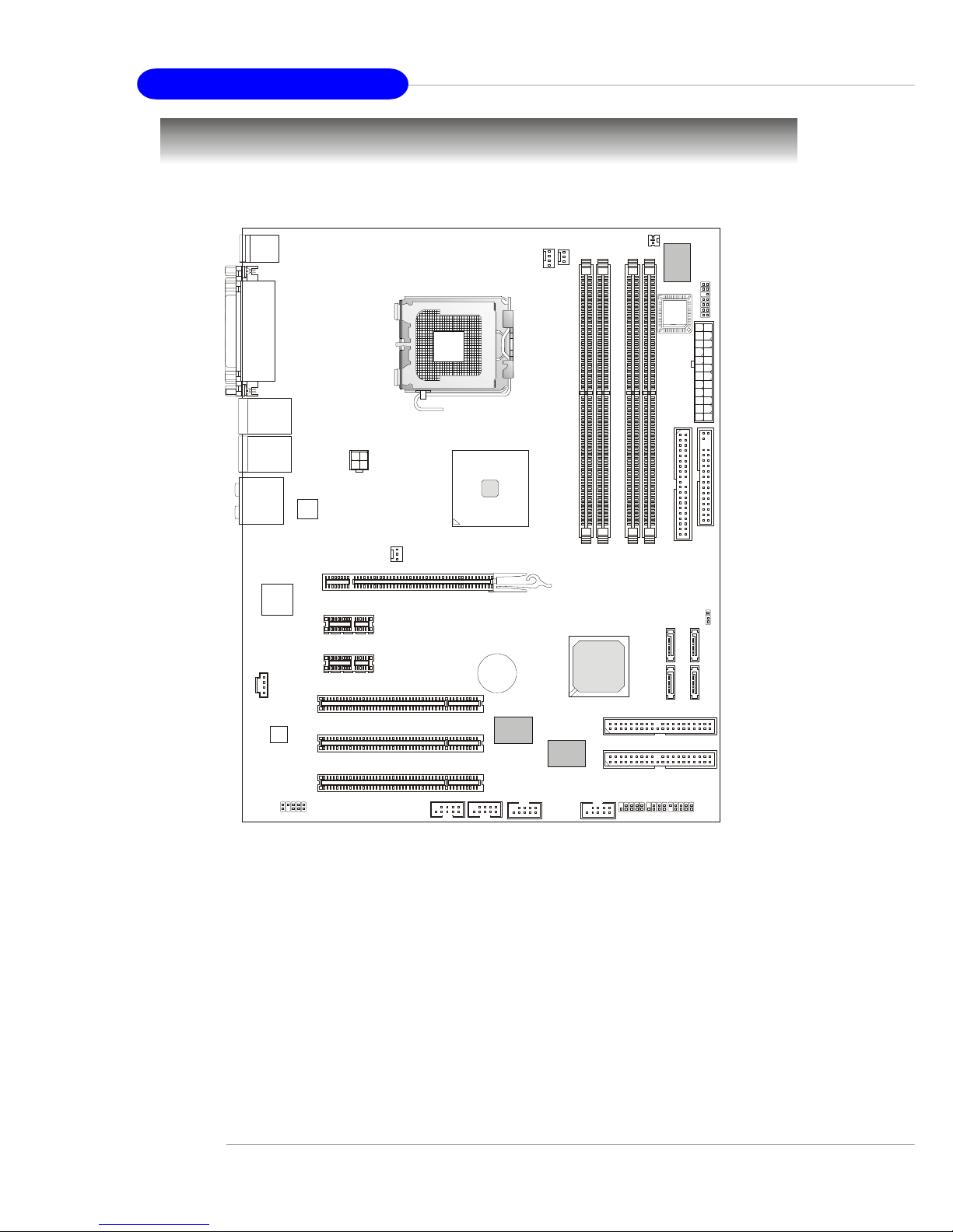
E-1-6
MS-7053 ATX Mainboard
Mainboard Layout
925X Neo Platinum (MS-7053) v1.X ATX Mainboard
NBFAN1
CPUFAN2
JC11
Intel
925X
JPW1
S
A
T
A
2
S
A
T
A
1
S
A
T
A
4
S
A
T
A
3
JCD1
BROADCOM
BCM5751KFB
T:
M:
B:
Line-In
Line-Out
Mic
T:RS-Out
M:CS
B:SPDIF Out
-Out
W
i
n
b
o
n
d
W
8
3
6
2
7
T
H
F
VIA
VT6410
VIA
VT6306
ICH6/
ICH6R
B
A
T
T
+
D
I
M
M
1
D
I
M
M
3
D
I
M
M
4
D
I
M
M
2
A
T
X
1
JLPC1
PCI 3
PCI 2
PCI 1
PCI_E3
PCI _E2
PCI_E1
IDE 2
I
D
E
1
F
D
D
1
IDE 3
JFP1
J
B
A
T
1
JFP2JDB1
JAUD1
JUSB1 JUSB2
J1394_2
(Optoinal)
J1394_3
(Optional)
Top : mouse
Bottom: keyboard
BIOS
T: LAN jack (Optiona l)
B: USB ports
Top : Parallel Port
Bottom:
COM A
1394 port (Optio n al)
SPDIF Out
CMI
9880L
T: LAN jack (Optiona l)
B: USB ports
SYSFAN2
Intel
82562EZ
Page 12

E-2-1
Hardware Setup
Chapter 2. Hardware Setup
This chapter tells you how to install the CPU, memory modules,
and expansion cards, as well as how to setup the jumpers on the
mainboard. Also, it provides the instructions on connecting the peripheral devices, such as the mouse, keyboard, etc.
While doing the installation, be careful in holding the components and follow the installation procedures.
Hardware Setup
Page 13
E-2-2
MS-7053 ATX Mainboard
Quick Components Guide
B
A
T
T
+
DDR DIMMs, p.2-7
IDE2, IDE3,
p.2-15
JFP2, p.2-17
Back Panel
I/O, p.2-10
CPUFAN1, p.2-14
ATX1, p.2-9
JFP1, p.2-17
PCI Slots 1~3,
p.2-23
JUSB1, JUSB2, p.2-19
JAUD1, p.2-18
SATA1~SATA4,
p.2-16
JDB1, p.2-21
J1394_2, J1394_3,
p.2-20
JCI1, p.2-20
JLPC1, p.2-19
JBAT1, p.2-22
JPW1, p.2-9
PCI Express x1,
p.2-23
PCI Express x16,
p.2-23
JCD1, p.2-18
NBFAN1, p.2-14
FDD1, p.2-14
IDE1, p.2-15
SYSFAN2, p.2-14
Page 14

E-2-3
Hardware Setup
Central Processing Unit: CPU
The mainboard supports Intel® Pentium 4 Prescott processor. The mainboard
uses a CPU socket called LGA775. When you are installing the CPU, make sure to
install the cooler to prevent overheating. If you do not have the CPU cooler,
contact your dealer to purchase and install them before turning on the computer.
For the latest information about CPU, please visit http://www.msi.com.tw/
program/products/mainboard/mbd/pro_mbd_cpu_support.php.
MSI Reminds You...
Overheating
Overheating will seriously damage the CPU and system, always make
sure the cooling fan can work properly to protect the CPU from
overheating.
Replacing the CPU
While replacing the CPU, always turn off the ATX power supply or
unplug the power supply’s power cord from grounded outlet first to
ensure the safety of CPU.
Overclocking
This motherboard is designed to support overclocking. However, please
make sure your components are able to tolerate such abnormal setting,
while doing overclocking. Any attempt to operate beyond product specifications is not recommended. We do not guarantee the damages
or risks caused by inadequate operation or beyond product
specifications.
Introduction to LGA 775 CPU
The surface of LGA 775 CPU.
Remember to apply some silicone heat transfer compound on
it for better heat dispersion.
Y ellow triangle is the Pin 1 indicator
The pin-pad side of LGA 775
CPU.
Y ellow triangle is the Pin 1 indicator
Alignment Key Alignment Key
Page 15

E-2-4
MS-7053 ATX Mainboard
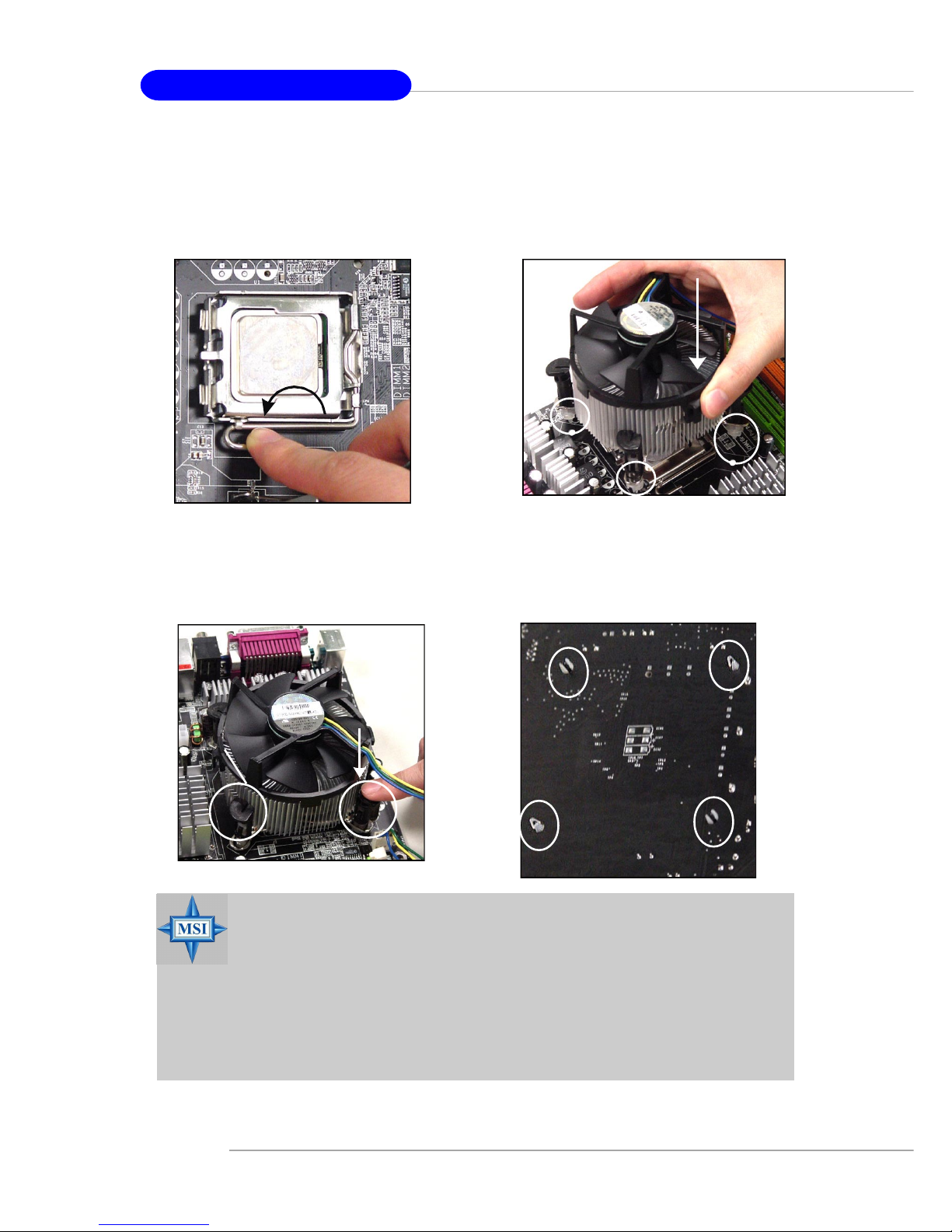
2. Remove the cap from lever hinge
side (as the arrow shows).
1. The CPU has a plastic cap on it to
protect the contact from damage.
Before you install the CPU, always
cover it to protect the socket pin.
3. The pins of socket reveal.
CPU & Cooler Installation
When you are installing the CPU, make sure the CPU has a cooler at-
tached on the top to prevent overheating. If you do not have the cooler, contact
your dealer to purchase and install them before turning on the computer. Meanwhile,
do not forget to apply some silicon heat transfer compound on CPU before installing
the heat sink/cooler fan for better heat dispersion.
Follow the steps below to install the CPU & cooler correctly. Wrong installation
will cause the damage of your CPU & mainboard.
4. Open the load lever.
Page 16
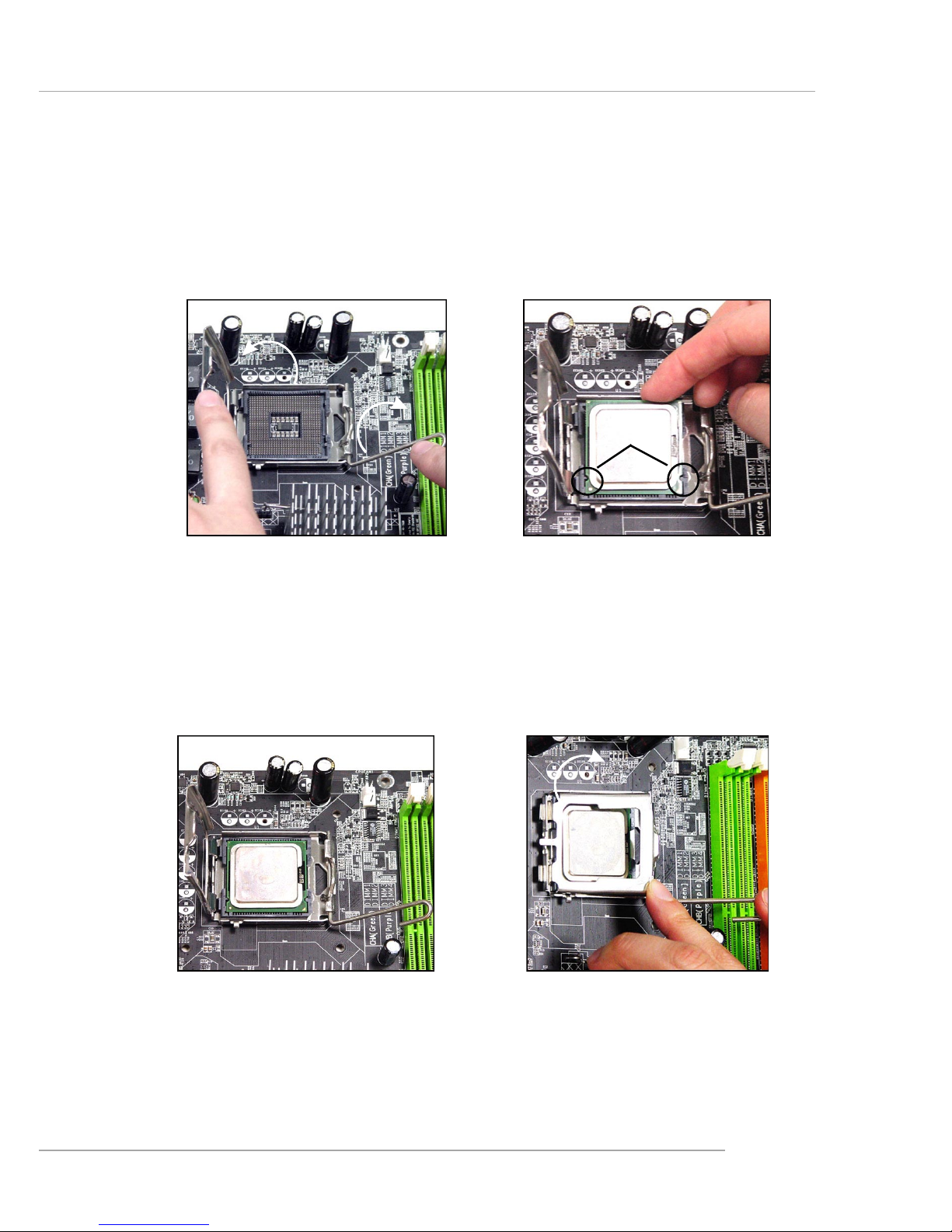
E-2-5
Hardware Setup
6. After confirming the CPU direction
for correct mating, put down the
CPU in the socket housing frame.
Be sure to grasp on the edge of
the CPU base. Note that the alignment keys are matched.
8. Cover the load plate onto the
package.
7. Visually inspect if the CPU is
seated well into the socket. If not,
take out the CPU with pure vertical
motion and reinstall.
alignment
key
5. Lift the load lever up and open the
load plate.
Page 17
E-2-6
MS-7053 ATX Mainboard
10. Align the holes on the mainboard
with the heatsink. Push down the
cooler until its four clips get
wedged into the holes of the
mainboard.
12.Turn over the mainboard to confirm that the clip-ends are correctly inserted.
11. Press the four hooks down to fasten the cooler. Then rotate the locking switch (refer to the correct direction marked on it) to lock the
hooks.
9. Press down the load lever lightly
onto the load plate, and then secure the lever with the hook under
retention tab.
locking
switch
MSI Reminds You...
1.Confirm if your CPU cooler is firmly installed before turning on your
system.
2.Do not touch the CPU socket pins to avoid damage.
3. Whenever CPU is not installed, always protect your CPU socket pin
with the plastic cap covered (shown in Figure 1) to avoid damage.
4. Please note that the mating/unmating durability of the CPU is 20
cycles. Therefore we suggest you do not plug/unplug the CPU too
often.
Page 18
E-2-7
Hardware Setup
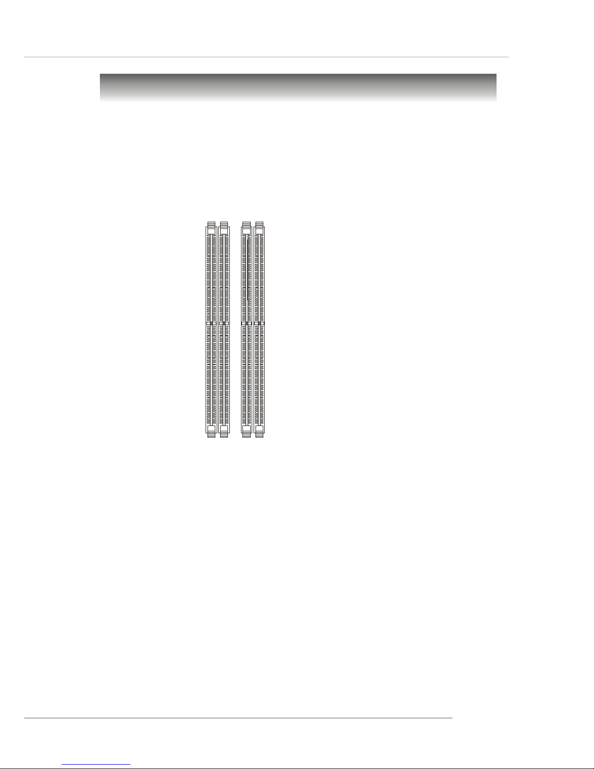
Memory
The mainboard provides 4 slots for 240-pin DDR2 DIMM, which supports the
memory size up to 4GB.
Since DDR2 modules are not interchangeable with DDR1 and the DDR2 standard is not backward compatible, you should always install DDR2 memory module in
the DDR2 slot (DIMM1~DIMM4). Otherwise, you are not able to boot up your system
and your mainboard might be damaged.
For the updated supporting memory modules, please visit http://www.msi.
com.tw/program/products/mainboard/mbd/pro_mbd_trp_list.php.
DIMM1~DIMM4
(from left to right)
Channel A (DIMM1, DIMM2): Green
Channel B (DIMM3, DIMM4): Orange
Introduction to DDR2 SDRAM
DDR2 is a new technology of memory module, and its speed is the top limit of
current DDR1 technology. DDR2 uses a 1.8V supply for core and I/O voltage, compared to 2.5V for DDR1, and requires 28% less power than DDR1 chips. DDR2 truly
is the future of memory, but will require some changes as the technology is not
backwardly compatible and only motherboards specifically designed for DDR2 memory
will be able to support these chips.
DDR2 incorporates new features at the chip level that give it better signal
integrity, thereby enabling higher clock speeds.
DDR2 modules have 240 pins, versus 184 pins on a DDR1 module, and the
length of DDR2 module is 5.25”. DDR2 modules have smaller and tighter spaced pins.
The height of DDR2 modules varies, but they will typically be less than 1.3” in height.
Page 19
E-2-8
MS-7053 ATX Mainboard
Installing DDR2 Modules
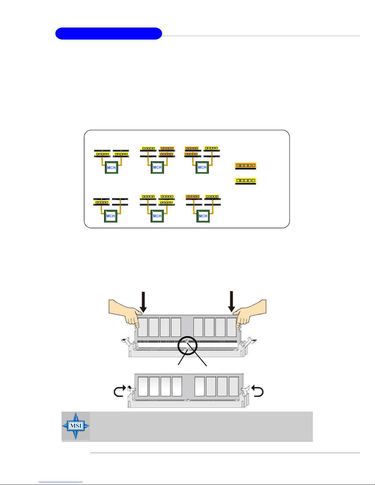
1. The DDR2 DIMM has only one notch on the center of module. The module will
only fit in the right orientation.
2. Insert the DIMM memory module vertically into the DIMM slot. Then push it in
until the golden finger on the memory module is deeply inserted in the socket.
3. The plastic clip at each side of the DIMM slot will automatically close.
Volt
Notch
Memory Module Population Rules
Install at least one DIMM module on the slots. Each DIMM slot supports up to a
maximum size of 1GB. Users can install either single- or double-sided modules to
meet their own needs. Please note that each DIMM can work respectively for
single-channel DDR, while both channels (in different color) populated
with same amount of memory size will work as dual-channel DDR, no matter
how many DIMM modules are populated.
Below are the example of single-channel/dual-channel DDR modes.
MSI Reminds You...
You can barely see the golden finger if the module is properly inserted in the socket.
Dual-channel mode
Single-channel mode
x MB
(ex: 128 MB)
2x MB
(ex: 256 MB)
Page 20
E-2-9
Hardware Setup
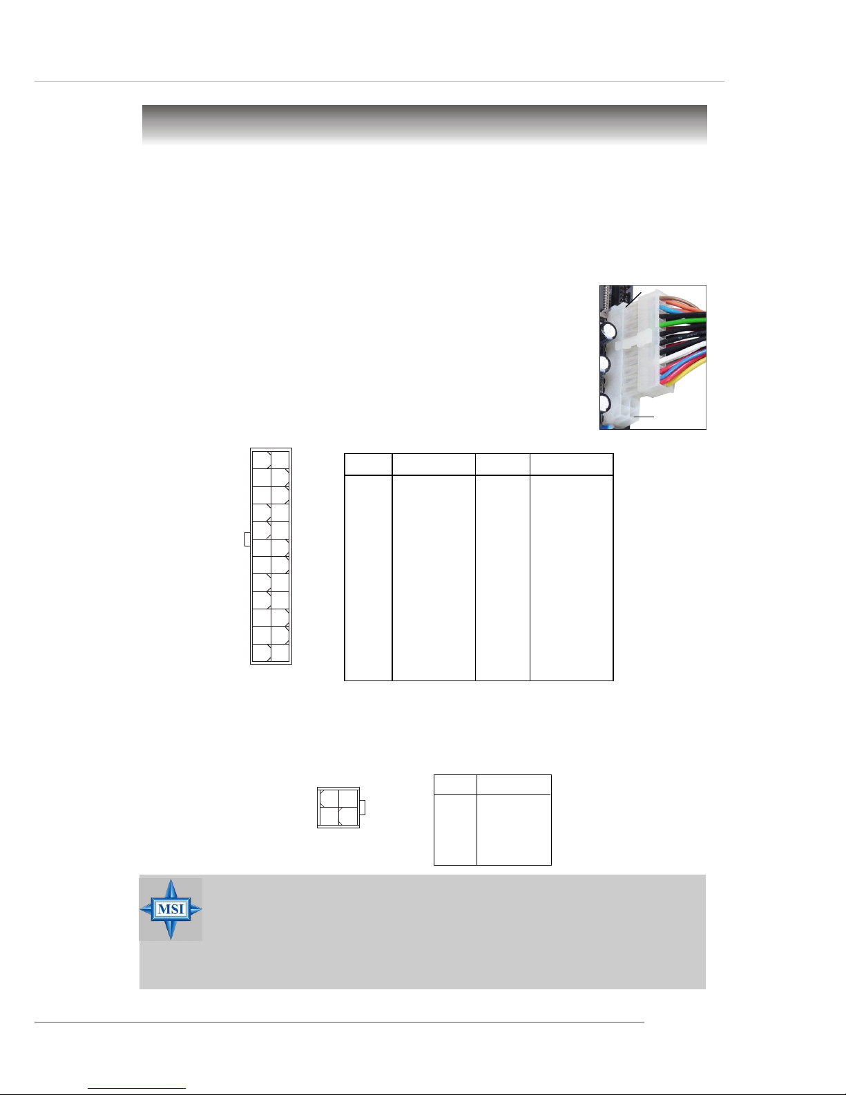
Power Supply
The mainboard supports ATX power supply for the power system. Before
inserting the power supply connector, always make sure that all components are
installed properly to ensure that no damage will be caused.
PIN SIGNAL
13 +3.3V
14 -12V
15 GND
1 6 PS-ON#
17 GND
18 GND
19 GND
20 Res
2 1 +5V
2 2 +5V
2 3 +5V
24 GND
PIN SIGNAL
1 +3.3V
2 +3.3V
3 GND
4 +5V
5 GND
6 +5V
7 GND
8 PWR OK
9 5VSB
10 +12V
11 +12V
12 NC
Pin Definition
PIN SIGNAL
1 GND
2 GND
3 12V
4 12V
JPW1 Pin Definition
ATX 12V Power Connector: JPW1
This 12V power connector is used to provide power to the CPU.
ATX 24-Pin Power Connector: ATX 1
This connector allows you to connect an ATX 24-pin power supply. To
connect the ATX 24-pin power supply, make sure the plug of the
power supply is inserted in the proper orientation and the pins are
aligned. Then push down the power supply firmly into the connector.
You may use the 20-pin ATX power supply as you like. If
you’d like to use the 20-pin ATX power supply, please plug your
power supply along with pin 1 & pin 13 (refer to the image at the
right hand). There is also a foolproof design on pin 11, 12, 23 & 24
to avoid wrong installation.
ATX1
1
12
24
13
pin 12
pin 13
MSI Reminds You...
1. These two connectors connect to the ATX power supply and have to
work together to ensure stable operation of the mainboard.
2. Power supply of 350 watts (and above) is highly recommended for
system stability.
3. ATX 12V power connection should be greater than 18A.
JPW1
13
42
Page 21
E-2-10
MS-7053 ATX Mainboard
USB Connectors
The mainboard provides an OHCI (Open Host Controller Interface) Universal
Serial Bus root for attaching USB devices such as keyboard, mouse or other USBcompatible devices. You can plug the USB device directly into the connector.
USB Ports
1 2 3 4
5 6 7 8
PIN SIGNAL DESCRIPTION
1 VCC +5V
2 -Data 0 Negative Data Channel 0
3 +Data0 Positive Data Channel 0
4 GND Ground
5 VCC +5V
6 -Data 1 Negative Data Channel 1
7 +Data 1 Positive Data Channel 1
8 GND Ground
USB Port Description
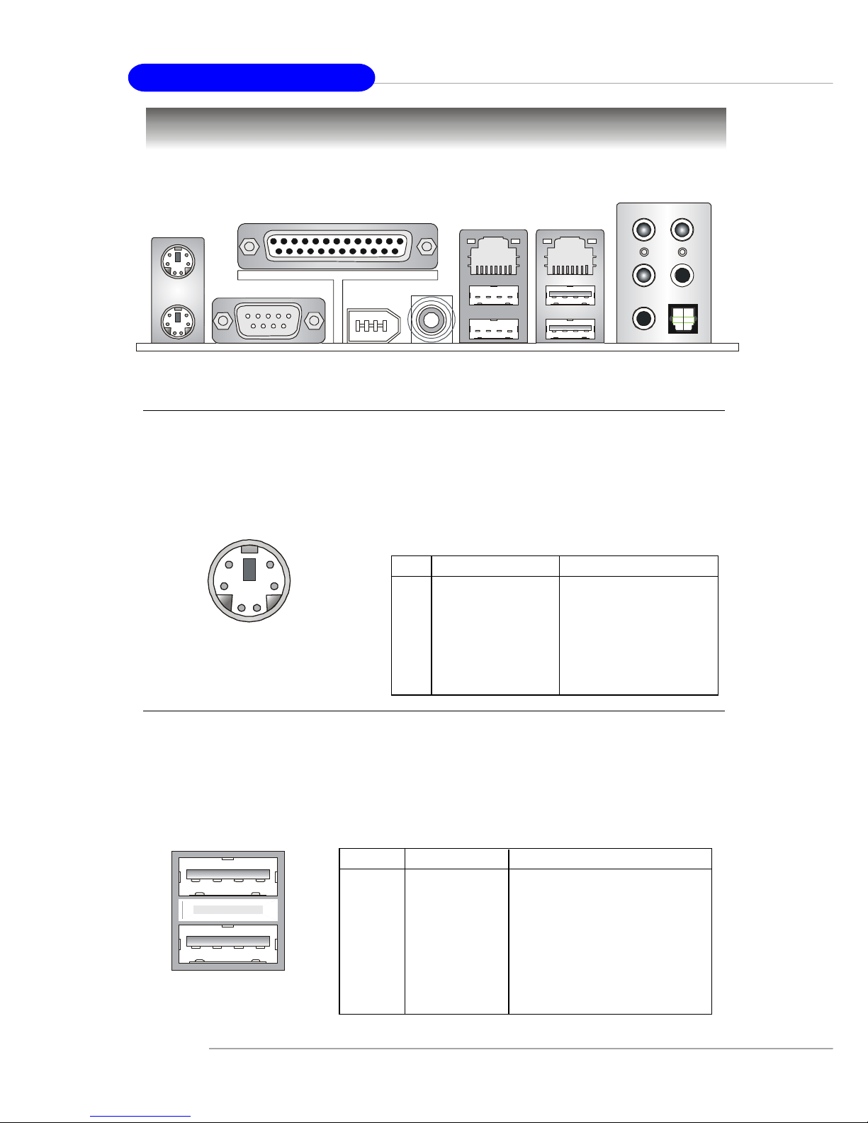
The back panel provides the following connectors:
Back Panel
Mouse/Keyboard Connector
The mainboard provides a standard PS/2® mouse/keyboard mini DIN connector
for attaching a PS/2® mouse/keyboard. You can plug a PS/2® mouse/keyboard directly
into this connector. The connector location and pin assignments are as follows:
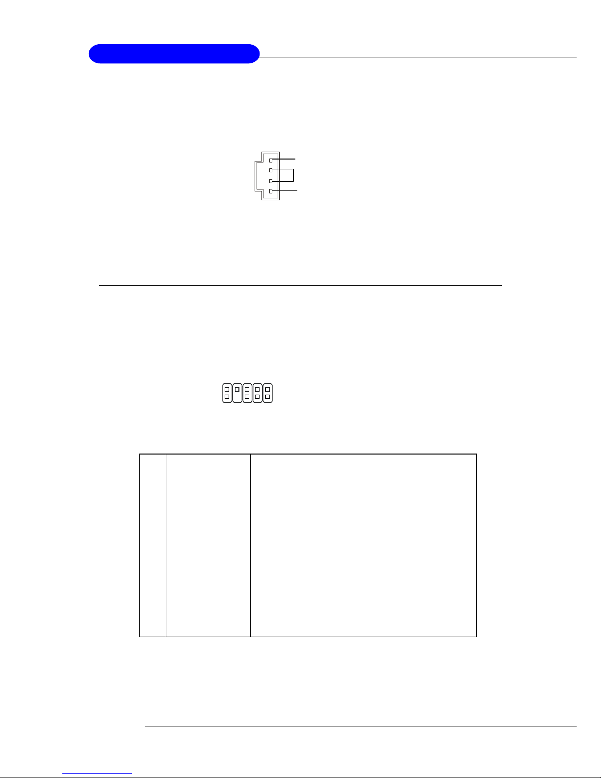
Keyboard
COM A
USB Ports
Mic
L-Out
L-In
Mouse
Parallel
Giga LAN
(Optional)
SPDIF
Out
RS-Out
SPDIF Out
CS-Out
10/100 LAN
(Optional)
1394 port
(Optional)
PIN SIGNAL DESCRIPTION
1 Mouse/Keyboard Data Mouse/Keyboard data
2 NC No connection
3 GND Ground
4 VCC +5V
5 Mouse/Keyboard Clock Mouse/Keyboard clock
6 NC No connection
Pin Definition
PS/2 Mouse / Keyboard
(6-pin Female)
2
1
3
4
5
6
Page 22
E-2-11
Hardware Setup
Serial Port Connector
The mainboard offers one 9-pin male DIN connector as the serial port. The port
is a 16550A high speed communication port that sends/receives 16 bytes FIFOs. You
can attach a serial mouse or other serial devices directly to the connector.
PIN SIGNAL DESCRIPTION
1 DCD Data Carry Detect
2 SIN Serial In or Receive Data
3 SOUT Serial Out or Transmit Data
4 DTR Data Terminal Ready)
5 GND Ground
6 DSR Data Set Ready
7 RTS Request T o Send
8 CTS Clear T o Send
9 RI Ring Indicate
Pin Definition
9-Pin Male DIN Connector
1 2 3 4 5
6 7 8 9
Audio Port Connectors
The left 3 audio jacks are for 2-channel mode for stereo speaker output: Line
Out is a connector for Speakers or Headphones. Line In is used for external CD
player, Tape player, or other audio devices. Mic is a connector for microphones.
However, there is an advanced audio application provided by CMI9880L to
offer support for 7.1-channel audio operation and can turn rear audio connectors
from 2-channel to 4-/5.1-channel audio.
S/PDIF Out-Coaxial
Rear Speaker Out
(in 7.1CH / 5.1CH)
Line Out
Line In
MIC
Center/Subwoofer
Speaker Out
( in 7.1CH / 5.1CH)
S/PDIF Out-Optical
(in 7.1CH / 5.1CH)
Page 23
E-2-12
MS-7053 ATX Mainboard
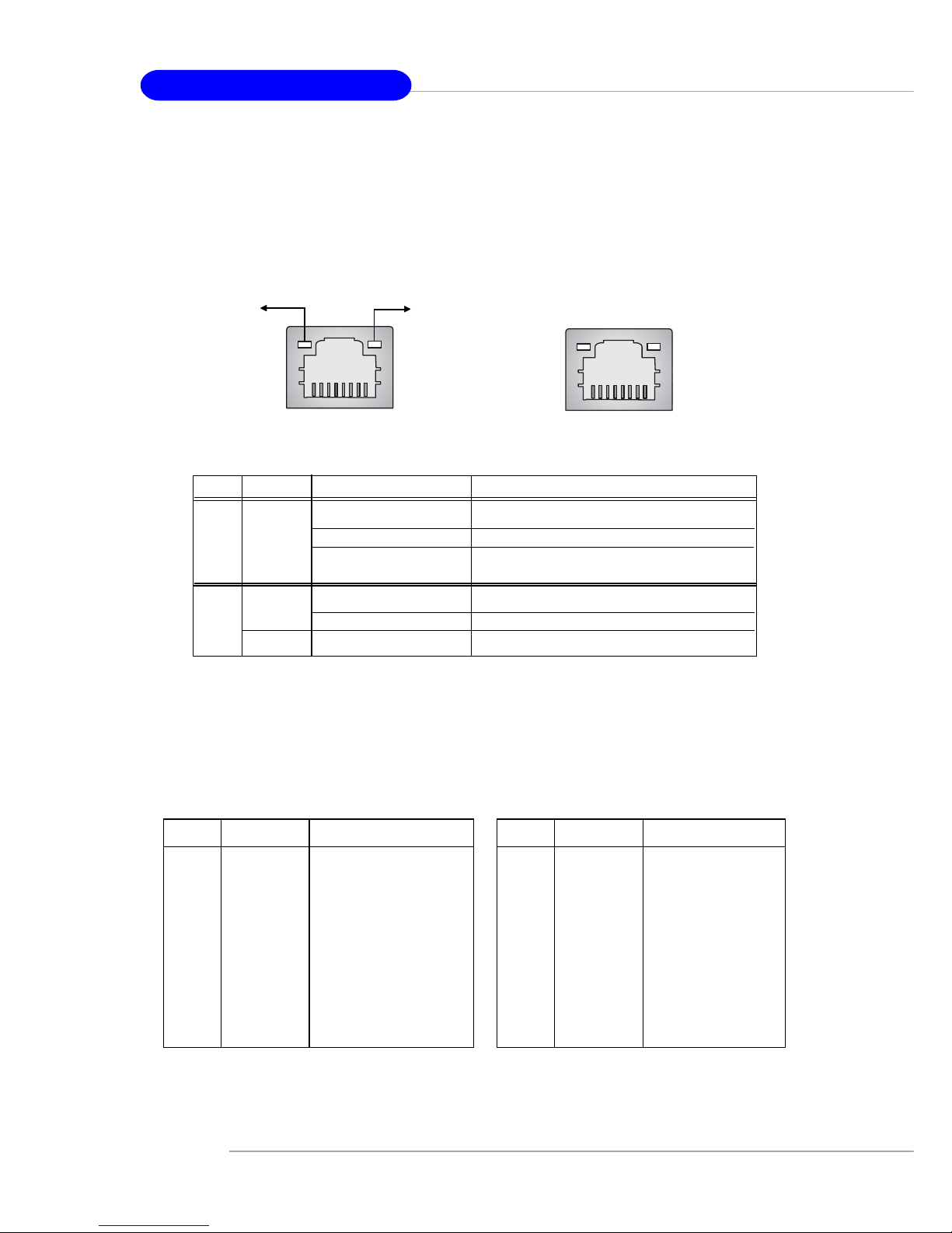
RJ-45 LAN Jack: 10/100 LAN (Intel 82562) / Giga-bit LAN (Broadcom
PCI-E) (Optional)
The mainboard provides two standard RJ-45 jacks for connection to Local
Area Network (LAN). Giga-bit LAN enables data to be transferred at 1000, 100 or
10Mbps. You can connect a network cable to either LAN jack.
The pin assignments vary depending on the transfer rates: 10/100Mbps or
1000Mbps. Note that Pin 1/2, 3/6, 4/5, 7/8 must work in pairs. Please refer
to the following for details:
LED Color LED State Condition
Off LAN link is not established.
Left Orange On (steady state) LAN link is established.
On (brighter & pulsing) The computer is communicating with another
computer on the LAN.
Green Off 10 Mbit/sec data rate is selected.
Right On 100 Mbit/sec data rate is selected.
Orange On 1000 Mbit/sec data rate is selected.
Link Indicator
8 1
Activity Indicator
RJ-45 10/100 LAN Jack
8 1
RJ-45 Giga-bit LAN Jack
10/100 LAN Pin Definition Giga-bit LAN Pin Definition
PIN SIGNAL DESCRIPTION
1 D0P Differential Pair 0+
2 D0N Differential Pair 0 3 D1P Differential Pair 1+
4 D2P Differential Pair 2+
5 D2N Differential Pair 2 6 D1N Differential Pair 1 7 D3P Differential Pair 3+
8 D3N Differential Pair 3-
PIN SIGNAL DESCRIPTION
1 TD P Transmit Differential Pair
2 TDN Transmit Differential Pair
3 RDP Receive Differential Pair
4 NC Not Used
5 NC Not Used
6 RDN Receive Differential Pair
7 NC Not Used
8 NC Not Used
Page 24
E-2-13
Hardware Setup
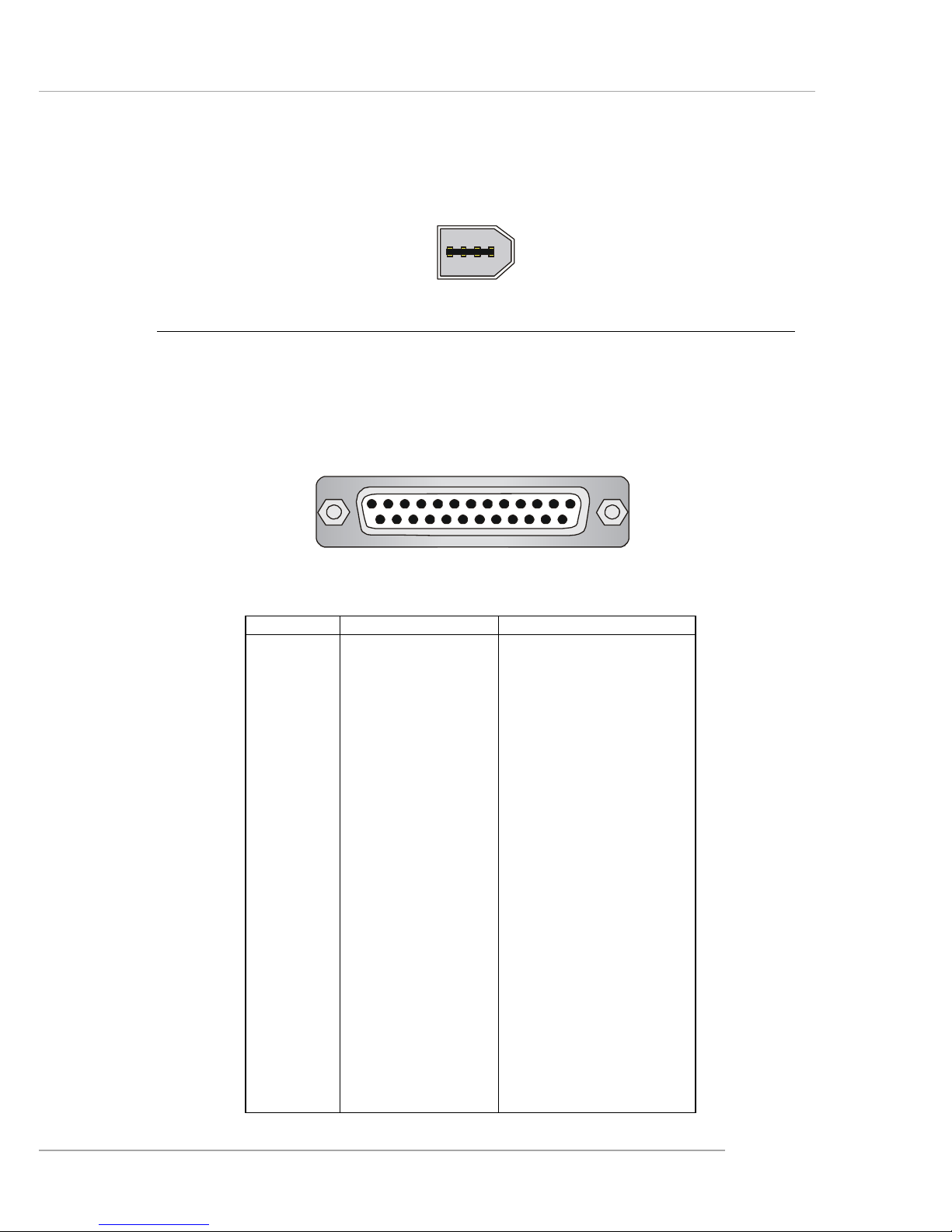
Parallel Port Connector: LPT1
The mainboard provides a 25-pin female centronic connector as LPT. A parallel
port is a standard printer port that supports Enhanced Parallel Port (EPP) and Extended Capabilities Parallel Port (ECP) mode.
PIN SIGNAL DESCRIPTION
1 STROBE Strobe
2 DATA0 Data0
3 DATA1 Data1
4 DATA2 Data2
5 DATA3 Data3
6 DATA4 Data4
7 DATA5 Data5
8 DATA6 Data6
9 DATA7 Data7
10 ACK# Acknowledge
11 BUSY Busy
12 PE Paper End
1 3 SELECT Select
1 4 AUTO FEED# Automatic Feed
15 ERR# Error
1 6 INIT# Initialize Printer
17 SLIN# Select In
18 GND Ground
19 GND Ground
20 GND Ground
21 GND Ground
22 GND Ground
23 GND Ground
24 GND Ground
25 GND Ground
Pin Definition
13 1
14
25
1394 Port (Optional)
There is one 1394 port on the back panel providing the connection for 1394
devices.
1394 port
Page 25
E-2-14
MS-7053 ATX Mainboard
The mainboard provides connectors to connect to FDD, IDE HDD, case, LAN,
USB Ports and CPU/System FAN.
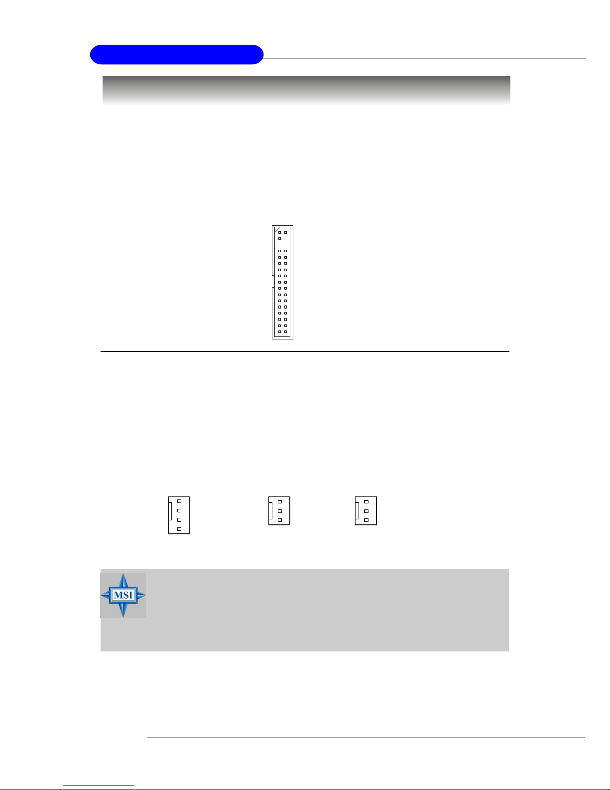
Floppy Disk Drive Connector: FDD1
The mainboard provides a standard floppy disk drive connector that supports
360K, 720K, 1.2M, 1.44M and 2.88M floppy disk types.
Connectors
FDD1
Fan Power Connectors: CPUF AN2/SYSFAN2/NBF AN1
The CPUFAN2 (processor fan), SYSFAN2 (system fan) and NBFAN1
(NorthBridge Chipset fan) support system cooling fan with +12V. It supports four/
three-pin head connector. When connecting the wire to the connectors, always take
note that the red wire is the positive and should be connected to the +12V, the black
wire is Ground and should be connected to GND. If the mainboard has a System
Hardware Monitor chipset on-board, you must use a specially designed fan with
speed sensor to take advantage of the CPU fan control.
NBFAN1
+12V
GND
NC
CPUFAN2
SENSOR
+12V
GND
Control
SYSFAN2
Sensor
+12V
GND
MSI Reminds You...
1. Always consult the vendors for proper CPU cooling fan.
2. CPUFAN2 supports fan control. CPU fan with 3 or 4 pins are both
available.
3. Please refer to the recommended CPU fans at Intel® official
website.
Page 26
E-2-15
Hardware Setup
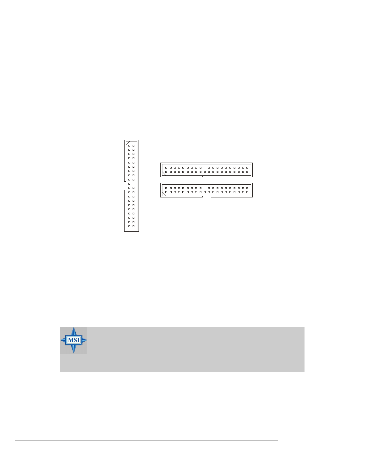
Hard Disk Connectors: IDE1, IDE2 & IDE3 (IDE 2 & IDE3 are optional)
The mainboard has one 32-bit Ultra DMA 66/100 IDE controller integrated in
ICH6/ICH6R, which supports PIO & Bus Master operation modes and it can connect
up to two Ultra ATA drives.
There is also another Ultra DMA 66/100/133 IDE controller integrated in the
optional VIA 6410 IDE Raid Controller, which supports RAID 0 & RAID 1, and can
connect up to four Ultra ATA 133 drives.
IDE1 (Primary IDE Connector)
The first hard drive should always be connected to IDE1. IDE1 can connect a Master
and a Slave drive. You must configure second hard drive to Slave mode by setting the
jumper accordingly.
IDE2, IDE3 (Third and Secondary IDE Connector)
IDE2 & IDE3 can also connect a Slave and a Master drive.
MSI Reminds You...
If you install two hard disks on cable, you must configure the second
drive to Slave mode by setting its jumper. Refer to the hard disk
documentation supplied by hard disk vendors for jumper setting
instructions.
IDE2 (yellow)
IDE3 (yellow)
IDE1 (blue)
Page 27
E-2-16
MS-7053 ATX Mainboard
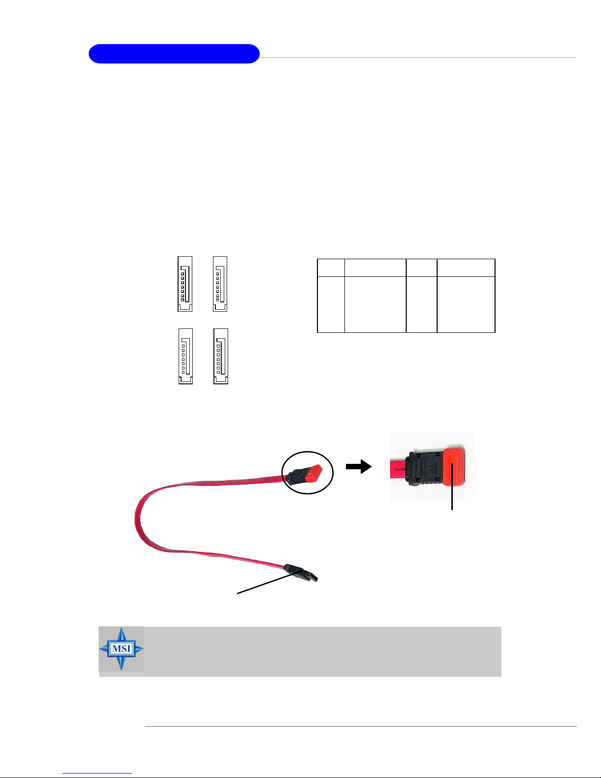
Serial ATA/Serial ATA RAID Connectors controlled by Intel ICH6/
ICH6R: SA TA1~SA T A4
The SouthBridge of this mainboard is Intel ICH6/ICH6R which supports four
serial ATA connectors SATA1~SATA4.
SATA1~SATA4 are dual high-speed Serial ATA interface ports. Each supports
1st generation serial ATA data rates of 150 MB/s. Both connectors are fully compliant
with Serial ATA 1.0 specifications. Each Serial ATA connector can connect to 1 hard
disk device.
PIN SIGNAL PIN SIGNAL
1 GND 2 TXP
3 TXN 4 GND
5 RXN 6 RXP
7 GND
SA TA1~ SA T A4 Pin Definition
MSI Reminds You...
Please do not fold the serial ATA cable in a 90-degree angle, since
this might cause the loss of data during transmission.
Connect to serial ATA ports
Take out the dust cover and
connect to the hard disk
devices
Serial A TA cable
SATA4
SATA3
1
7
SATA2
SATA1
1
7
Page 28
E-2-17
Hardware Setup
Front Panel Connectors: JFP1 & JFP2
The mainboard provides two front panel connectors for electrical connection
to the front panel switches and LEDs. JFP2 is compliant with Intel® Front Panel I/O
Connectivity Design Guide.
PIN SIGNAL DESCRIPTION
1 HD_LED_P Hard disk LED pull-up
2 FP PWR/SLP MSG LED pull-up
3 HD_LED_N Hard disk active LED
4 FP PWR/SLP MSG LED pull-up
5 RST_SW_N Reset Switch low reference pull-down to GND
6 PWR_SW_P Power Switch high reference pull-up
7 RST_SW_P Reset Switch high reference pull-up
8 PWR_SW_N Power Switch low reference pull-down to GND
9 RSVD_DNU Reserved. Do not use.
JFP2 Pin Definition
PIN SIGNAL PIN SIGNAL
1 GND 2 SPK3 SLED 4 BUZ+
5 PLED 6 BUZ7 NC 8 SPK+
JFP1 Pin Definition
1
2
9
10
JFP1
HDD
LED
Reset
Switch
Power
LED
Power
Switch
7
8
Power LED
Speaker
1
2
JFP2
Page 29
E-2-18
MS-7053 ATX Mainboard
Front Panel Audio Connector: JAUD1
The JAUD1 front panel audio connector allows you to connect to the front
panel audio and is compliant with Intel® Front Panel I/O Connectivity Design Guide.
CD-In Connector: JCD1
The connector is for CD-ROM audio connector.
JAUD1
1
2
9
10
JCD1
GND
R
L
PIN SIGNAL DESCRIPTION
1 PORT 1L Analog Port 1 - Left channel
2 GND Ground
3 PORT 1R Analog Port 1 - Right channel
4 PRESENCE# Active low signal - signals BIOS that a High Definition Audio
dongle is connected to the analog header. PRESENCE# = 0
when a High Definition Audio dongle is connected.
5 PORT 2R Analog Port 2 - Right channel
6 SENSE1_RETIRN Jack detection return from front panel JACK1
7 SENSE_SEND Jack detection sense line from the High Definition Audio CODEC
jack detection resistor network
8 KEY Connector Key
9 PORT 2L Analog Port 2 - Left channel
1 0 SENSE2_RETIRN Jack detection return from front panel JACK2
JAUD1 Pin Definition
Page 30
E-2-19
Hardware Setup
Connected to JUSB1
or JUSB2
USB 2.0 Bracket
(Optional)
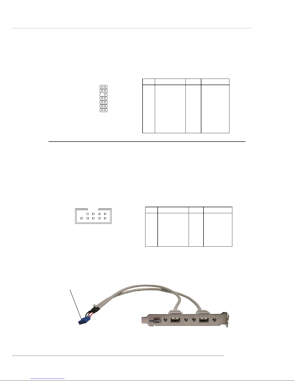
Front USB Connectors: JUSB1 & JUSB2
The mainboard provides two standard USB 2.0 pin headers JUSB1 & JUSB2 .
USB 2.0 technology increases data transfer rate up to a maximum throughput of
480Mbps, which is 40 times faster than USB 1.1, and is ideal for connecting highspeed USB interface peripherals such as USB HDD, digital cameras, MP3 players,
printers, modems and the like.
JLPC1 Pin Definition
PIN SIGNAL PIN SIGNAL
1 LCLK 2 Key (no pin)
3 LRST# 4 VCC3
5 LAD0 6 FID0_LRST
7 LAD1 8 VCC5
9 LAD2 10 Key (no pin)
11 LAD3 12 GND
13 LFRAME# 14 GND
PIN SIGNAL PIN SIGNAL
1 VCC 2 VCC
3 USB0- 4 USB15 USB0+ 6 USB1+
7 GND 8 GND
9 Key (no pin) 10 USBOC
JUSB1 & JUSB2 Pin Definition
JUSB1, JUSB2
(USB 2.0)
1
2 10
9
FWH/LPC Debugging Pin Header: JLPC1
The pin header is for internal debugging only.
JLPC1
13
14
2
1
Page 31

E-2-20
MS-7053 ATX Mainboard
IEEE 1394 Connectors: J1394_2, J1394_3 (Optional)
The mainboard provides two 1394 pin headers that allow you to connect IEEE
1394 ports via an external IEEE1394 bracket.
Pin Definition
PIN SIGNAL PIN SIGNAL
1TPA+ 2 TPA3 Ground 4 Ground
5 TPB+ 6 TPB7 Cable power 8 Cable power
9 Key (no pin) 10 Ground
J1394_2~J1394_3
1
2
9
10
IEEE1394 Bracket (Optional)
Foolproof Design
Chassis Intrusion Switch Connector: JCI1
This connector is connected to a 2-pin chassis switch. If the chassis is opened,
the switch will be short. The system will record this status and show a warning
message on the screen. To clear the warning, you must enter the BIOS utility and
clear the record.
JCI1
CINTRU
GND
1
Page 32

E-2-21
Hardware Setup
D-Bracket™ 2 Connector: JDB1
The mainboard comes with a JDB1 connector for you to connect to D-Bracket™
2. D-Bracket™ 2 is a USB Bracket that supports both USB1.1 & 2.0 spec. It integrates
four LEDs and allows users to identify system problem through 16 various combinations of LED signals.
D-Bracket™ 2
(Optional)
Connected to JDB1
LEDs
Connected to JUSB1
or JUSB2
Pin Signal
1 DBG1 (high for green color)
2 DBR1 (high for red color)
3 DBG2 (high for green color)
4 DBR2 (high for red color)
5 DBG3 (high for green color)
6 DBR3 (high for red color)
7 DBG4 (high for green color)
8 DBR4 (high for red color)
9 Key
10 N C
Pin Definition
JDB1
1
9
2
10
Page 33

E-2-22
MS-7053 ATX Mainboard
Jumpers
MSI Reminds You...
You can clear CMOS by shorting 2-3 pin while the system is off.
Then return to 1-2 pin position. Avoid clearing the CMOS while the
system is on; it will damage the mainboard.
JBAT1
1
Clear Data
3
1
Keep Data
3
1
The motherboard provides the following jumpers for you to set the computer’s
function. This section will explain how to change your motherboard’s function through
the use of jumpers.
Clear CMOS Jumper: JBA T1
There is a CMOS RAM on board that has a power supply from external battery
to keep the system configuration data. With the CMOS RAM, the system can automatically boot OS every time it is turned on. If you want to clear the system configuration,
use the JBAT1 (Clear CMOS Jumper ) to clear data. Follow the instructions below to
clear the data:
Page 34

E-2-23
Hardware Setup
Slots
The mainboard provides one PCI Express x16 slot, two PCI Express x1 slots,
and three 32-bit PCI bus slots.
PCI Slots
PCI Express x1 slot
PCI Express x16 slot
PCI Express Slots
The PCI Express slots, as a high-bandwidth, low pin count, serial, interconnect technology, support Intel highest performance desktop platforms utilizing the
Intel Pentium 4 processor with HT Technology.
PCI Express architecture provides a high performance I/O infrastructure for
Desktop Platforms with transfer rates starting at 2.5 Giga transfers per second over
a PCI Express x1 lane for Gigabit Ethernet, TV Tuners, 1394 controllers, and general
purpose I/O. Also, desktop platforms with PCI Express Architecture will be designed
to deliver highest performance in video, graphics, multimedia and other sophisticated
applications. Moreover, PCI Express architecture provides a high performance graphics
infrastructure for Desktop Platforms doubling the capability of existing AGP8x designs with transfer rates of 4.0 GB/s over a PCI Express x16 lane for graphics
controllers, while PCI Express x1 supports transfer rate of 250 MB/s.
You can insert the expansion cards to meet your needs. When adding or
removing expansion cards, make sure that you unplug the power supply first.
PCI (Peripheral Component Interconnect) Slots
The PCI slots allow you to insert the expansion cards to meet your needs.
When adding or removing expansion cards, make sure that you unplug the power
supply first. Meanwhile, read the documentation for the expansion card to make any
necessary hardware or software settings for the expansion card, such as jumpers,
switches or BIOS configuration.
The orange PCI slot (PCI3) supports 2 masters, therefore it can also works as
a communication slot. You may install the communication card on this slot, such as the
wireless LAN PCI cards of MSI.
Page 35

E-2-24
MS-7053 ATX Mainboard
PCI Interrupt Request Routing
The IRQ, acronym of interrupt request line and pronounced I-R-Q, are hard-
ware lines over which devices can send interrupt signals to the microprocessor. The
PCI IRQ pins are typically connected to the PCI bus INT A# ~ INT D# pins as follows:
Order 1 Order 2 Order 3 Order 4
PCI Slot 1 INT A# INT B# INT C# INT D#
PCI Slot 2 INT B# INT C# INT D# INT A#
PCI Slot 3 INT C# INT D# INT A# INT B#
Page 36

E-3-1
BIOS Setup
Chapter 3. BIOS Setup
BIOS Setup
This chapter provides information on the BIOS Setup program
and allows you to configure the system for optimum use.
You may need to run the Setup program when:
An error message appears on the screen during system boot up, and
requests you to run SETUP.
You want to change the default settings for customized features.
MSI Reminds You...
1. The items under each BIOS category described in this chapter are
under continuous update for better system performance.
Therefore, the description may be slightly different from the latest
BIOS and should be held for reference only.
2. While booting up, the BIOS version is shown in the 1st line appearing after the memory count. It is usually in the format:
example: W7030MS V1.1 040104
where:
1st digit refers to BIOS maker as A=AMI(R); W=AWARD(R)
2nd - 5th digit refers to the model number.
6th - 7th digit refers to the customer, MS=all standard customers.
V2.0 refers to the BIOS version.
040104 refers to the date this BIOS is released.
Page 37

E-3-2
MS-7053 ATX Mainboard
Entering Setup
Power on the computer and the system will start POST (Power On Self Test) process.
When the message below appears on the screen, press <DEL> key to enter Setup.
Press DEL to enter SETUP
If the message disappears before you respond and you still wish to enter Setup,
restart the system by turning it OFF and On or pressing the RESET button. You may
also restart the system by simultaneously pressing <Ctrl>, <Alt>, and <Delete> keys.
Selecting the First Boot Device
You are allowed to select the 1st boot device without entering the BIOS setup utility
by pressing <F11>. When the same message as listed above appears on the screen,
press <F11> to trigger the boot menu.
The POST messages might pass by too quickly for you to respond in time. If so,
restart the system and press <F11> after around 2 or 3 seconds to activate the boot
menu similar to the following.
The boot menu will list all the bootable devices. Select the one you want to boot from
by using arrow keys, then press <Enter>. The system will boot from the selected
device. The selection will not make changes to the settings in the BIOS setup utility,
so next time when you power on the system, it will still use the original first boot
device to boot up.
Select First Boot Device
Floppy : 1st Floppy
IDE-0 : IBM-DTLA-307038
CDROM : ATAPI CD-ROM DRIVE 40X M
[Up/Dn] Select [RETURN] Boot [ESC] cancel
Page 38

E-3-3
BIOS Setup
Control Keys
Getting Help
After entering the Setup menu, the first menu you will see is the Main Menu.
Main Menu
The main menu lists the setup functions you can make changes to. You can use the
arrow keys ( ↑↓ ) to select the item. The on-line description of the highlighted setup
function is displayed at the bottom of the screen.
Sub-Menu
If you find a right pointer symbol (as shown in the right view) appears to the left of
certain fields, that means a sub-menu can be launched from this field. A sub-menu
contains additional options for a field parameter. You can use arrow keys ( --> ) to
highlight the field and press <Enter> to call up the submenu. Then you can use the control keys to enter values and move from field to field within a sub-menu. If
you want to return to the main menu, just press <Esc >.
General Help <F1>
The BIOS setup program provides a General Help screen. You can call up this screen
from any menu by simply pressing <F1>. The Help screen lists the appropriate keys
to use and the possible selections for the highlighted item. Press <Esc> to exit the
Help screen.
<↑> Move to the previous item
<↓> Move to the next item
<←> Move to the item in the left hand
<→> Move to the item in the right hand
<Enter> Select the item
<Esc> Jumps to the Exit menu or returns to the main menu from a
submenu
<+/PU> Increase the numeric value or make changes
<-/PD> Decrease the numeric value or make changes
<F6> Load Fail-Safe Defaults
<F7> Load Optimized Defaults
<F10> Save all the CMOS changes and exit
Page 39

E-3-4
MS-7053 ATX Mainboard
The Main Menu
Standard CMOS Features
Use this menu for basic system configurations, such as time, date etc.
Advanced BIOS Features
Use this menu to setup the items of AWARD® special enhanced features.
Advanced Chipset Features
Use this menu to change the values in the chipset registers and optimize your system’s
performance.
Integrated Peripherals
Use this menu to specify your settings for integrated peripherals.
Power Management Setup
Use this menu to specify your settings for power management.
PNP/PCI Configurations
This entry appears if your system supports PnP/PCI.
H/W Monitor
This entry shows the status of your CPU, fan, warning for overall system status.
Cell Menu
Use this menu to specify your settings for CPU / DRAM / PCI / PCI Express frequency/
voltage control and overclocking.
Load Fail-Safe Defaults
Use this menu to load factory default settings into the BIOS for stable system performance operations.
Once you enter Phoenix-Award® BIOS CMOS Setup Utility, the Main Menu will appear
on the screen. The Main Menu allows you to select from the eleven setup functions
and two exit choices. Use arrow keys to select among the items and press <Enter>
to accept or enter the sub-menu.
Page 40

E-3-5
BIOS Setup
Load Optimized Defaults
Use this menu to load the BIOS values for the best system performance, but the
system stability may be affected.
BIOS Setting Password
Use this menu to set the password for BIOS.
Save & Exit Setup
Save changes to CMOS and exit setup.
Exit Without Saving
Abandon all changes and exit setup.
Page 41

E-3-6
MS-7053 ATX Mainboard
Advanced Chipset Features
DRAM Timing Selectable
Selects whether DRAM timing is controlled by the SPD (Serial Presence Detect) EEPROM
on the DRAM module. Setting to [Auto By SPD] enables DRAM timings and the following related items to be determined by BIOS based on the configurations on the SPD.
Selecting [Manual] lets users configure the DRAM timings and the following related
items manually. Setting options: [Manual], [Auto By SPD], [Turbo], [Ultra].
CAS Latency Time
This controls the CAS latency, which determines the timing delay (in clock cycles)
before SDRAM starts a read command after receiving it. Settings: [Auto], [2], [2.5],
[3]. [2] increases the system performance the most while [3] provides the most stable
performance.
DRAM RAS# to CAS# Delay
When DRAM is refreshed, both rows and columns are addressed separately. This
setup item allows you to determine the timing of the transition from RAS (row address
strobe) to CAS (column address strobe). The less the clock cycles, the faster the
DRAM performance. Setting options: [Auto], [2], [3], [4], [5].
DRAM RAS# Precharge
This item controls the number of cycles for Row Address Strobe (RAS) to be allowed
to precharge. If insufficient time is allowed for the RAS to accumulate its charge
before DRAM refresh, refresh may be incomplete and DRAM may fail to retain data.
This item applies only when synchronous DRAM is installed in the system. Setting
options: [Auto], [2], [3], [4], [5].
Precharge delay (tRAS)
This setting determines the precharge delay, which determines the timing delay for
DRAM precharge. Setting options: [Auto], [4], [5], [6], [7], [8], [9], [10], [11], [12], [13],
[14], [15].
Page 42

E-3-7
BIOS Setup
System BIOS Cacheable
Selecting [Enabled] allows caching of the system BIOS ROM at F0000h-FFFFFh,
resulting in better system performance. However, if any program writes to this
memory area, a system error may result. Setting options: [Enabled], [Disabled].
Video BIOS Cacheable
Selecting [Enabled] allows caching of the video BIOS ROM at C0000h to C7FFFh,
resulting in better video performance. However, if any program writes to this memory
area, a system error may result. Setting options: [Enabled], [Disabled].
Memory Hole
In order to improve performance, certain space in memory can be reserved for ISA
peripherals. This memory must be mapped into the memory space below 16MB. When
this area is reserved, it cannot be cached. Settings: [Disabled], [Enabled].
PCI Express Root Port Function
Press <Enter> to enter the sub-menu and the following screen appears:
PCI Express Port 1/2/3/4
These items allow you to enable or disable the controllers of each PCI Express port.
PCI Express Port 1: the controller of onboard Giga Lan
PCI Express Port 2: reserved
PCI Express Port 3: the controller of PCI-E slot 3 (PCI_E2)
PCI Express Port 4: the controller of PCI-E slot 4 (PCI_E3)
Setting options: [Enabled], [Disabled], [Auto].
PCI-E Compliancy Mode
This item allows you to select the supported spec of PCI Express x1 slot. Setting
options: [v1.0], [v1.0a].
DRAM Data Integrity Mode
Set this option according to the type of DRAM installed in your system: error-correcting code (ECC) or parity (default). Setting optoins: [ECC], [Non-ECC].
Page 43

E-3-8
MS-7053 ATX Mainboard
PATA IDE Mode
This item allows you to select the parallel ATA channel. Setting options:[Primary],
[Secondary].
SATA Port
This feature allows users to view the SATA port as primary or secondary channel.
On-Chip Serial ATA
(Combined)
SATA Only [SATA 1/3/2/4]
PATA Pri, SATA Sec [IDE1, SATA2/4]
SATA Pri, PATA Sec [SATA1/3, IDE1]
PATA Only [IDE1]
On-Chip Serial ATA
(Enhanced)
IDE [IDE1, SATA 1/2/3/4]
AHCI [IDE1, SATA 1/2/3/4]
RAID [IDE1, SATA 1/2/3/4],
[SATA support RAID 0 or 1]
SATA Devices Configuration
Press <Enter> to enter the sub-menu and the following screen appears:
SATA Mode, On-Chip Serial ATA
These 2 items allow you to select the SATA and the ATA/IDE configuration.
For the setting options of SATA Mode, select [IDE] if you want to have SATA as IDE
function. Select [AHCI] to allow the SATA to have Advanced Host Controller Interface
(AHCI) feature, which supports improved serial ATA disk performance with native
command queuing & native hot plug. Select [RAID] to use SATA as RAID function.
Setting options: [IDE], [AHCI], [RAID].
For the setting options of On-Chip Serial ATA, select [Disabled] if you want to
disable both SATA controller. Select [Combined Mode] or [Enhanced Mode] to use the
IDE, S-ATA and P-ATA devices. Select [Auto] to let the system arrange automatically.
Select [SATA Only] to let the SATA operate in legacy mode. Refer to the following
tables for details.
SATA Device Configuration
Page 44

E-3-9
BIOS Setup
PNP/PCI Configurations
This section describes configuring the PCI bus system and PnP (Plug & Play) feature.
PCI, or Peripheral Component Interconnect, is a system which allows I/O devices to
operate at speeds nearing the speed the CPU itself uses when communicating with
its special components. This section covers some very technical items and it is
strongly recommended that only experienced users should make any changes to the
default settings.
Init Display First
This setting specifies which VGA card is your primary graphics adapter. Setting
options are:
[PCI Ex] The system initializes the PCI Express graphic first. If a PCI Ex-
press graphic card is not available, it will initialize the PCI graphic
card.
[PCI Slot] The system initializes the PCI Graphic card first. If a PCI Graphic
card is not available, it will initialize the PCI Express graphic.
PCI Slot1 IRQ, PCI Slot2 IRQ, PCI Slot3 IRQ
These items specify the IRQ line for each PCI slot. Setting options: [3], [4], [5], [7], [9],
[10], [11], [12], [14], [15], [Auto]. Selecting [Auto] allows BIOS to automatically determine the IRQ line for each PCI slot.
**PCI Express relative items**
Maximum Payload Size
This item allows you to set the maximum TLP (transaction layer packet) payload size
for the PCI Express devices. Setting options: [128], [256], [512], [1024], [2048], [4096].
MSI Reminds You...
IRQ (Interrupt Request) lines are system resources allocated to I/O
devices. When an I/O device needs to gain the attention of the operating
system, it signals this by causing an IRQ to occur. After receiving the
signal, when the operating system is ready, the system will interrupt itself
and perform the service required by the I/O device.
Page 45

E-3-10
MS-7053 ATX Mainboard
CPU Smart Fan Temperature
When the current temperature of the CPU fan reaches the value you specify here,
the CPU fan will speed up for cooling down to avoid the CPU damage; on the contrary,
if the CPU fan current temperature is lower than the specified value, the CPU fan will
slow down its speed to keep the temperature stable.
CPU Temperature Tolerance
You can select a fan tolerance value here for the specific range for the CPU Smart
Fan Temperature item. If the current temperature of the CPU fan reaches the
maximum threshold (the temperature set in the CPU Smart Fan Temperature plus
the tolerance value you set here), the fan will speed up for cooling down. On the
contrary if the current temperature reaches the minimum threshold (the set temperatures minus the tolerance value), the fan will slow down to keep the temperatures
stable.
PC Health Status
Press <Enter> and the following sub-menu appears.
H/W Monitor
This section shows the status of your CPU, fan, overall system status, etc. Monitor
function is available only if there is hardware monitoring mechanism onboard.
System/CPU Temperature, Current System Fan Speed, Vcore(V), +5 V,
+5VSB
These items display the current status of all of the monitored hardware devices/
components such as CPU voltage, temperatures and all fans’ speeds.
Page 46

E-3-11
BIOS Setup
Cell Menu
The items in Cell Menu includes some important settings of CPU, PCI Express, DRAM
and overclocking functions.
Current CPU Clock
These two items show the current clocks of CPU. Read-only.
High Performance Mode
This item allows you to select the CPU/FSB parameters. Setting options: [Manual],
[Optimized]. When [Optimized] is selected, the system will use overclocked CPU/FSB
parameters. Select [Manual] for normal mode CPU/FSB parameters.
Dynamic OverClocking
Dynamic Overclocking Technology is the automatic overclocking function, included in
the MSITM’s newly developed CoreCell
TM
Technology. It is designed to detect the load
balance of CPU while running programs, and to adjust the best CPU frequency
automatically. When the motherboard detects that CPU is running programs, it will
speed up CPU automatically to make the program run smoothly and faster. When the
CPU is temporarily suspending or staying in the low load balance, it will restore the
default settings. Usually the Dynamic Overclocking Technology will be powered only
when users' PC need to run huge amount of data like 3D games or the video process,
and the CPU frequency need to be boosted up to enhance the overall performance.
Setting options:
[Disabled] Disable Dynamic Overclocking function.
[Private] 1st level of overclocking, increasing the CPU frequency by 1%.
[Sergeant] 2nd level of overclocking, increasing the CPU frequency by 3%.
[Captain] 3rd level of overclocking, increasing the CPU frequency by 5%.
[Colonel] 4th level of overclocking, increasing the CPU frequency by 7%.
[General] 5th level of overclocking, increasing the CPU frequency by 10%.
[Commander] 6th level of overclocking, increasing the CPU frequency by 15%.
MSI Reminds You...
Change these settings only if you are familiar with the chipset.
Page 47

E-3-12
MS-7053 ATX Mainboard
Adjust CPU Ratio
This item allows you to adjust the CPU ratio. Setting range is from [8] to [50].
Adjust DDR Frequency
This item allows you to set an artificial memory clock limit on the system. Please note
that memory is prevented from running faster than this frequency. Setting options:
[DDR 333], [DDR 400], [DDR 533], [Auto].
Auto Detect PCI Clk
This item is used to auto detect the PCI slots. When set to [Enabled], the system will
remove (turn off) clocks from empty PCI slots to minimize the electromagnetic interference (EMI). Settings: [Enabled], [Disabled].
Spread Spectrum
When the motherboard’s clock generator pulses, the extreme values (spikes) of the
pulses creates EMI (Electromagnetic Interference). The Spread Spectrum function
reduces the EMI generated by modulating the pulses so that the spikes of the pulses
are reduced to flatter curves. If you do not have any EMI problem, leave the setting at
[Disabled] for optimal system stability and performance. But if you are plagued by EMI,
select the desired range for EMI reduction. Remember to disable Spread Spectrum
function if you are overclocking, because even a slight jitter can introduce a temporary
boost in clock speed which may just cause your overclocked processor to lock up.
CPU Clock
This item allows you to select the CPU Front Side Bus clock frequency (in MHz) and
overclock the processor by adjusting the FSB clock to a higher frequency. Setting
options: For CPU FSB200: [200]~[500]
For CPU FSB133: [133]~[500]
MSI Reminds You...
1. Even though the Dynamic Overclocking Technology is more stable
than manual overclocking, basically, it is still risky. We suggest
user to make sure that your CPU can afford to overclock regularly
first. If you find the PC appears to be unstable or reboot
incidentally, it's better to disable the Dynamic Overclocking or to
lower the level of overclocking options. By the way, if you need to
conduct overclocking manually, you also need to disable the Dynamic OverClocking first.
2. Meanwhile, there are two functions to protect user's system from
crashing.
- There is a safe key "Ins" in BIOS. In case the overclocking
fails, you can press "Ins" key while system rebooting to
restore to the BIOS defaults.
- If the system incidentally reboot for four times, the BIOS will
also be restored to the defaults.
Page 48

E-3-13
BIOS Setup
CPU Voltage
The settings are used to adjust the CPU clock multiplier (ratio) and CPU core voltage
(Vcore). These settings offer users a tool to overclock the system. Setting options:
[By CPU Default], [1.18v]~[1.49v].
Memory Voltage
Adjusting the DDR voltage can increase the DDR speed. Any changes made to this
setting may cause a stability issue, so changing the DDR voltage for long-term
purpose is NOT recommended.
AGP/PCI Express Voltage
AGP voltage and PCI Express voltage are both adjustable in their individual fields,
allowing you to increase the performance of your AGP display card/PCI Express card
when overclocking, but the stability may be affected.
MSI Reminds You...
The settings shown in different color in CPU Voltage, Memory Voltage and AGP/PCI Express Voltage help to verify if your setting is
proper for your system.
Gray: Default setting.
Yellow: High performance setting.
Red: Not recommended setting and the system may be
unstable.
Changing CPU Voltage, Memory Voltage and AGP/PCI Express
Voltage may result in the instability of the system; therefore, it is NOT
recommended to change the default setting for long-term usage.
Page 49

E-3-14
MS-7053 ATX Mainboard
Load Fail-Safe/Optimized Defaults
The two options on the main menu allow users to restore all of the BIOS settings to
the default Fail-Safe or Optimized values. The Optimized Defaults are the default
values set by the mainboard manufacturer specifically for optimal performance of the
mainboard. The Fail-Safe Defaults are the default values set by the BIOS vendor for
stable system performance.
When you select Load Fail-Safe Defaults, a message as below appears:
Pressing Y loads the BIOS default values for the most stable, minimal system
performance.
When you select Load Optimized Defaults, a message as below appears:
Pressing Y loads the default factory settings for optimal system performance.
Page 50

F-1-1
Introduction
925X Neo
User’s Guide
French
Page 51

F-1-2
Carte Mère ATX MS-7053
Page 52

F-1-3
Introduction
Chapter 1. Getting
Started
TFélicitation vous venez d’acheter une carte mère 925X Neo
Platinum (MS-7053) v1.X ATX. La 925X Neo Platinum est basée
sur les chipsets Intel® 925X et Intel® ICH6/ICH6R procurant de
hautes performances. Conçue pour les proceseurs Intel® Pentium
Prescott LGA775, la 925X Neo Platinum apportera satisfaction
tant aux particuliers qu’aux professionnels.
Introduction
Page 53

F-1-4
Carte Mère ATX MS-7053
Spécificités de la Carte
CPU
h Supporte les processeurs Intel® Pentium 4 Prescott LGA775.
h Supporte Pentium 4 3XX, 5XX & 7XX ou supérieur.
h Supporte la technologie Intel Hyper-Threading.
(Pour connaître les dernières informations sur le CPU, veuillez visiter http://www.
msi.com.tw/program/products/mainboard/mbd/pro_mbd_cpu_support.php)
Chipset
h Chipset Intel® 925X
- Supporte FSB 800MHz.
- Supporte l’interface PCI Express x16.
- Supporte l’interface mémoire DDR2 400/533.
h Chipset Intel® ICH6/ICH6R
- Contrôleur ultra rapide USB (USB2.0), 480Mb/sec, jusqu’à 8 ports.
- 4 ports Serial ATA avec un taux de transfert de 1.5Gb/s.
- 1 contrôleur canal Ultra ATA 100 bus Master IDE.
- PCI Master v2.3, I/O APIC.
- Compatible ACPI 2.0.
- Serial ATA 150 RAID 0, RAID 1 et Matrix RAID (pour ICH6R uniquement).
- Contrôleur AHCI integré (pour ICH6R uniquement).
Mémoire principale
h Supporte quatre DIMM unbuffered de DDR2 1.8 Volt
h Supporte un maximum de mémoire de 4GB.
h Supporte l’architecture mémoire double canal DDR2.
h Supporte l’interface mémoire DDR2 400/533.
(Pour une mise ŕ jour sur les modules de mémoires supportés, veuillez visiter http://
www.msi.com.tw/program/products/mainboard/mbd/pro_mbd_trp_list.php.)
Slots
h Un slot PCI Express x16 (supporte les spécifications PCI Express Bus v1.0a).
h Deux PCI Express x1 slots (supporte les spécifications PCI Express Bus v1.0a).
h Troisslots 32-bit v2.3 Master PCI bus (supportant l’interface 3.3v/5v PCI bus).
IDE Integré
h Un contrôleur Ultra DMA 66/100 IDE integré dans l’ICH6/ICH6R.
- Supporte les modes opératoires PIO, Bus Master.
- Possibilité de connecter jusqu’à deux matériels Ultra ATA.
h Contrôleur Serial ATA 150 integré dans l’ICH6/ICH6R.
- Taux de transfert jusqu’à 150MB/sec.
- Possibilité de connecter jusqu’à quatre matériels Serial ATA.
- Supporte contrôleur AHCI avec SATA Raid 0, Raid 1 et Matrix Raid (pour ICH6R
uniquement).
- Supporte le SATA hot plug (pour ICH6R uniquement).
Page 54

F-1-5
Introduction
Contrôleur RAID IDE VIA6410
h Deux contrôleurs IDE DMA 66/100/133.
h Supporte RAID 0, 1 et 0+1.
h Possibilité de connecter jusqu’ŕ 4 matériels Ultra ATA 133.
Périphériques Intégrés
h Les périphériques intégrés sont :
- 1 port floppy supportant 1 FDD avec 360K, 720K, 1.2M, 1.44M et 2.88Mbytes
- 1 port série
- 1 port 1394 (Optionnel)
- 1 port parallèle supportant les modes SPP/EPP/ECP
- 1 Line-In / Line-Out / MIC-In / Rear Speaker Out / Center-Subwoofer Speaker Out
/ SPDIF-Out optical and coaxial audio port
- 8 ports USB (Arrière * 4/ Façade * 4)
- 2 RJ-45 LAN jack (Optionnel)
LAN (Optionnel)
h Contrôleur Broadcom BCM5751 PCI-E Gb LAN
- Compatible PCI Express bus Spec 1.0a.
- Interface x1 PCI Express avec bande passante 2.5 Gb/s.
- Compatible 10/100/1000 IEEE 802.3.
h Contrôleur LAN Intel 82562EZ 10/100 PHY
- Compatible 10/100 IEEE 802.1.
Audio
h Contrôleur Azalia link intégré dans le chipset Intel® ICH6/ICH6R.
h Codec audio 8 canaux CMI9880L.
- Compatible avec l’Azalia 1.0 Spec.
- Supporte la fonction multi canaux.
- Supporte l’Universal Audio Jack (uniquement pour le Jack Audio Front).
BIOS
h La carte mère utilise un BIOS “Plug & Play” détectant les périphériques ainsi que
les cartes d’extension de façon automatique.
h La carte offre une fonction DMI (Desktop Management Interface) qui enregistre les
spécifications de la carte mère.
Montage et Dimensions
h Format ATX : 24.4 cm (W) x 30.5 cm (L)
h 9 trous de montage
Page 55

F-1-6
Carte Mère ATX MS-7053
Schéma de la Carte Mère
Carte Mère ATX 925X Neo Platinum (MS-7053) v1.X
NBFAN1
CPUFAN2
JC11
Intel
925X
JPW1
S
A
T
A
2
S
A
T
A
1
S
A
T
A
4
S
A
T
A
3
JCD1
BROADCOM
BCM5751KFB
T:
M:
B:
Line-In
Line-Out
Mic
T:RS-Out
M:CS
B:SPDIF Out
-Out
W
i
n
b
o
n
d
W
8
3
6
2
7
T
H
F
VIA
VT6410
VIA
VT6306
ICH6/
ICH6R
B
A
T
T
+
D
I
M
M
1
D
I
M
M
3
D
I
M
M
4
D
I
M
M
2
A
T
X
1
JLPC1
PCI 3
PCI 2
PCI 1
PCI_E3
PCI _E2
PCI_E1
IDE 2
I
D
E
1
F
D
D
1
IDE 3
JFP1
J
B
A
T
1
JFP2JDB1
JAUD1
JUSB1 JUSB2
J1394_2
(Optoinal)
J1394_3
(Optional)
Top : mouse
Bottom: keyboard
BIOS
T: LAN jack (Optiona l)
B: USB ports
Top : Parallel Port
Bottom:
COM A
1394 port (Optio n al)
SPDIF Out
CMI
9880L
T: LAN jack (Optiona l)
B: USB ports
SYSFAN2
Intel
82562EZ
Page 56

F-2-1
Installation Matériel
Chapter 2. Hardware Setup
Ce chapitre vous donne des indications sur l’installation du
CPU, des modules de mémoire, les cartes d’extension, ainsi que sur
la configuration des cavaliers de la carte mčre. Vous retrouverez
aussi des instructions pour la connexion de périphériques (souris,
clavier ...).
Lors de l’installation, veuillez vous prémunir contre l’electricité
statiques et veuillez suivre les procédures d’installation afin de mettre
en place correctement les différents composants.
Installation Matériel
Page 57

F-2-2
Carte Mère ATX MS-7053
Guide des Composants
B
A
T
T
+
DDR DIMMs, p.2-7
IDE2, IDE3,
p.2-15
JFP2, p.2-17
Panneau
Arrière I/O,
p.2-10
CPUFAN1, p.2-14
ATX1, p.2-9
JFP1, p.2-17
Slots PCI 1~3,
p.2-23
JUSB1, JUSB2, p.2-19
JAUD1, p.2-18
SATA1~SATA4,
p.2-16
JDB1, p.2-21
J1394_2, J1394_3,
p.2-20
JCI1, p.2-20
JLPC1, p.2-19
JBAT1, p.2-22
JPW1, p.2-9
PCI Express x1,
p.2-23
PCI Express x16,
p.2-23
JCD1, p.2-18
NBFAN1, p.2-14
FDD1, p.2-14
IDE1, p.2-15
SYSFAN2, p.2-14
Page 58

F-2-3
Installation Matériel
Central Processing Unit: CPU
La carte mère supporte les processeurs Intel® Pentium 4 Prescott. La carte mère
utilise un socket CPU appelé LGA775. Quand vous avez installé votre CPU, assurez
vous que le CPU possède un système de reffroidissement pour prévenir
les risques de surchauffre. Si vous n’avez pas de ventilateur, veuillez contacter
vote revendeur qui vous conseillera.
Pour connaître les dernières informations relatives au CPU, veuillez visiter http://
www.msi.com.tw/program/products/mainboard/mbd/pro_mbd_cpu_support.php.
MSI Vous Rappelle...
Surchauffe
Une surchauffe peut sérieusement endommager le CPU et le système,
assurez vous toujours que le système de reffroidissement fonctionne
correctement pour protéger le CPU d’une surchauffe.
Remplacer le CPU
Avant de remplacer le CPU, éteignez toujours l’alimentation ATX ou
débranchez la prise pour assurer la sécurité du CPU.
Overclocking
Cette carte mère a été créée pour supporter l’overclocking. Assurez
vous que vos composants sont capables de tolérer de tels réglages,
avant d’overclocker le système. Tout essais au delà des spécifications
des produits n’est pas recommandé. Nous ne garantissons pas les
damages causés par une mauvaises opération ou au delà des
spécifications du produit.
Introduction au LGA 775 CPU
Dessus du CPU LGA 775.
Ne pas oublier de mettre de la
pâte thermique pour une
meilleure dissipation thermique.
Le triangle jaune est le premier
indicateur
Dessous du CPU LGA 775.
Le triangle jaune est le premier
indicateur
Alignment Key Alignment Key
Page 59

F-2-4
Carte Mère ATX MS-7053
2. Retirer le capot comme indiqué
(dans le sens indiqué par la flèche).
1. Le CPU possède un capot plastique
le protégeant. Ne jamais retirer le
capot avant que le CPU ne soit
installé.
3. Les broches du socket sont
Installer le système de refroidissement du CPU
Quand vous installerez votre CPU, assurez vous que le CPU possède
un système de reffroidissement pour prévenir les surchauffes. Si vous
ne possédez pas de système de reffroidissement, contactez votre
revendeur pour vous en procurer un et installez le avant d’allumer
l’ordinateur.
4. Ouvrir le levier.
visibles.
Page 60

F-2-5
Installation Matériel
6. Après verification du CPU, appuyez
dessus pour qu’il se connecte au
socket. Verifiez en même temps
que l’alignement est correct.
8. Refermer le plateau.
7. Regarder si le CPU est bien
positionné dans le socket. Si non,
retirez le CPU et installez le de
nouveau.
alignment
key
5.Tirer le levier et ouvrir le plateau.
Page 61

F-2-6
Carte Mère ATX MS-7053
10. Aligner les trous de la carte mère
avec le ventilateur. Appuyer sur le
ventilateur jusqu’à ce que les clips
soient dans les trous de la carte.
12.Retourner la carte mère pour
s’assurer que les clips sont bine
insérés.
11. Appuyer sur le 4 parties (comme
indiqué) puis effectuer une rotation (se référer aux marque) pour
sécuriser l’ensemble.
9. Abaisser le levier, puis le sécuriser
en l’attachant au mécanisme de
rétention.
locking
switch
MSI Vous Rappelle...
1. Vérifier la connexion du ventilateur de CPU avant de démarre le PC.
2. Ne pas toucher les broches du CPU pour éviter de les endommager.
3. Si vous e^te amné ŕ retirer votre CPU, ne pas oublier de remettre la
protection (capot) en plastique sur le socket (voir figure 1).
4. A noter que la mise en place du CPU est prévue pour une vingtaine
de connexion, cependant il n’est pas recommandé d’installer/retirer
le CPU trop souvent.
Page 62

F-2-7
Installation Matériel
Mémoire
La carte mère procure 4 slots DDR2 240 broches, supportant un maximum de
mémoire de 4GB.
Vu que les modules de DDR2 ne sont pas interchangeables avec la DDR1, et
que la DDR2 n’est pas compatible avec la DDR1, vous devez alors installer des
modules de mémoire DDR2 sur les slots (DIMM1~DIMM4). Dans le cas contraire vous
ne pourrez pas démarrer le PC et votre carte mère pourrait être endommagée.
Pour mettre à jour la liste des mémoires supportées, veuillez visiter http://
www.msi.com.tw/program/products/mainboard/mbd/pro_mbd_trp_list.php.
DIMM1~DIMM4
(de gauche à droite)
Canal A (DIMM1, DIMM2): Vert
Canal B (DIMM3, DIMM4): Orange
Introduction à la DDR2 SDRAM
La DDR2 est une nouvelle technologie pour la mémoire. La DDR2 utilise une
alimentation 1.8V pour le core et le voltage I/O, contre 2.5V pour la DDR1, ce qui
représente un gain d’énergie de 28%. La DDR2 est la mémoire de nouvelle génération,
mais elle nécessite certaines modifications puisqu’elle n’est pas compatible avec la
DDR1.
La DDR2 incorpore de nouvelles fonctionnalités, permettant d’obtenir des
cycles d’horloge plus elevés.
Les modules de DDR2 possèdent 240 broches, contre 184 pour la DDR1 et
mesurent 5.25”.
Page 63

F-2-8
Carte Mère ATX MS-7053
Installer des Modules DDR2
1. Le DIMM DDR ne possčde qu’une encoche en son centre. Ainsi il n’est possible de
monter le module que dans un seul sens.
2. Insérez le module de mémoire DIMM verticalement dans le slot. Puis appuyez
dessus
3. Le clip en plastique situé de chaque cōté du module va se fermer automatiquement.
Volt
Encoche
Règle de Population des Mémoires
Il faut au moins installer un slot de mémoire pour que le système puisse
fonctionner. fonctionner. Chaque slot DIMM peut supporter un maximum de 1GB.
Users can install either single- or double-sided modules to meet their own needs.
Chaque DIMM peut fonctionner en simple canal DDR, cependant si tous les
DIMM de mémoire sont utilisés ou seulement 2 (de couleurs différentes) et
que la quantité de mémoire est identique, alors vous pourrez fonctionner
en mode double canal DDR. Ci-dessous un exemple de mémoire simple ou double
canal DDR.
MSI Vous Rappelle...
La marque dorée doit ą peine źtre visible lorsque le module est
correctement installé.
Mode double canal
Mode simple canal
x MB
(ex: 128 MB)
2x MB
(ex: 256 MB)
Page 64

F-2-9
Installation Matériel
Alimentation
La carte supporte les alimentations ATX. Avant de connecter l’alimentation, assurezvous que tous les composants sont bien installés afin d’éviter de les endommager.
PIN SIGNAL
13 +3.3V
14 -12V
15 GND
16 PS-ON#
17 GND
18 GND
19 GND
20 Res
21 +5V
22 +5V
23 +5V
24 GND
PIN SIGNAL
1 +3.3V
2 +3.3V
3 GND
4 +5V
5 GND
6 +5V
7 GND
8 PWR OK
9 5VSB
10 +12V
11 +12V
12 N C
Pin Definition
PIN SIGNAL
1 GND
2 GND
3 12V
4 12V
JPW1 Pin Definition
Connecteur d’Alimentation ATX 12V : JPW1
Ce connecteur d’alimentation 12V permet l’alimentation du CPU.
Connecteur d’Alimentation A TX 24 broches : ATX1
Ce connecteur permet la connexion d’alimentations ATX 24 broches. Pour la
connexion, assurez-vous que le bloc blanc de l’alimentation est
correctement positionné. Puis appuyez dessus afin que la connexion
soit réalisée.
Vous pouvez utiliserune alimentation ATX 20 broches. Si
vous utilisez une alimentation 20 broches vérifiez bien que vous
vous connectez sur les broches 1 & 13 (voir photo). Il existe un
systčme prévu pour éviter une mauvaise connexion sur les brohes
11, 12, 23 & 24.
ATX1
1
12
24
13
pin 12
pin 13
JPW1
13
42
MSI Vous Rappelle...
1. Ces deux connecteurs assurent la bonne alimentation du système et
assurent la stabilité de ce dernier.
2. Nous vous recommandons d’utiliser une alimentation de 350 watts
(ou supérieur) pour assurer la stabilité.
3. La connexion ATX 12V doit être supérieure à 18A.
Page 65

F-2-10
Carte Mère ATX MS-7053
Connecteurs USB
La carte possède un OHCI (open Host Controller Interface) Bus Universel Série
permettant la connnexion de matériels USB (clavier, souris...). Vous pouvez brancher
directement vos produits USB sur ce connecteur.
USB Ports
1 2 3 4
5 6 7 8
PIN SIGNAL DESCRIPTION
1 VCC +5V
2 -Data 0 Negative Data Channel 0
3 +Data0 Positive Data Channel 0
4 GND Ground
5 VCC +5V
6 -Data 1 Negative Data Channel 1
7 +Data 1 Positive Data Channel 1
8 GND Ground
USB Port Description
Le panneau arričre procure les connecteurs suivants :
Panneau Arrière
Connecteur Clavier/Souris
La carte procure un connecteur Din standard pour souris PS/2® et pour clavier. Vous
pouvez brancher directement votre souris ou clavier sur les connecteurs :
Clavier
COM A
Ports USB
Mic
L-Out
L-In
Souris
Parallèle
SPDIF
Out
RS-Out
SPDIF Out
CS-Out
PIN SIGNAL DESCRIPTION
1 Mouse/Keyboard Data Mouse/Keyboard data
2 NC No connection
3 GND Ground
4 VCC +5V
5 Mouse/Keyboard Clock Mouse/Keyboard clock
6 NC No connection
Pin Definition
Clavier/Souris PS/2
(6-pin Female)
2
1
3
4
5
6
Giga LAN
(Optionnel)
10/100 LAN
(Optionnel)
1394 port
(Optionnel)
Page 66

F-2-11
Installation Matériel
Connecteur Port Série
La carte mère possède un connecteur 9 broches male (port série). Le port est
un port de communication 16550A qui envoie/reçcoit 16 bytes FIFOs. Vous pouvez y
brancher une souris série ou n’importe quel autre appareils série.
PIN SIGNAL DESCRIPTION
1 DCD Data Carry Detect
2 SIN Serial In or Receive Data
3 SOUT Serial Out or Transmit Data
4 D TR Data Terminal Ready)
5 G ND Ground
6 D SR Data Set Ready
7 RTS Request To Send
8 CTS Clear To Send
9 RI Ring Indicate
Pin Definition
Connecteur 9-Pin Male DIN
1 2 3 4 5
6 7 8 9
Audio Port Connectors
Les 3 conecteur de gauche sont utilisés pour la fonction 2 canaux (stéréo):
Line Out est destiné aux enceintes ou écouteurs. Line In est prévu pour la connexion
d’un matériel extérieur tel que lecteur CD. Mic est utilisé pour la connexion d’un
microphone.
Cependant il existe une application audio avancée qui est procurée par
CMI9880L pour offrir du son 7.1.
S/PDIF Out-Coaxial
Sortie des
enceintes arrières
(in 7.1CH / 5.1CH)
Line Out
Line In
MIC
Center/Subwoofer
Speaker Out
( in 7.1CH / 5.1CH)
S/PDIF en sortie
optique
(in 7.1CH / 5.1CH)
Page 67

F-2-12
Carte Mère ATX MS-7053
RJ-45 LAN Jack: 10/100 LAN (Intel 82562) / Giga-bit LAN (Broadcom
PCI-E) (Optionnel)
La cartre mère possède en option un connecteur jack RJ-45 permettant de se
connecter à un LAN (Local Area Network). Le Giga-bit LAN permet aux données
d’être transferées à des vitesses de 1000, 100 ou 10Mbps. Vous pouvez connecter
un câble LAN sur ce jack
L’assignation des broches varie selon le taux de transfert: 10/100Mbps ou
1000Mbps. A noter que les broches 1/2, 3/6, 4/5, 7/8 doivent fonctionner par paires.
Veuillez vous reporter aux détails ci-dessous :
LED Color Etat de la LED Condition
Off Lien réseau non établi.
Gauche Orange On (steady state) Lien réseau établi.
On (brighter & pulsing) Le PC communique avec un autre PC sur le réseau
Vert Off Taux de transfert selectionné 10 Mbit/sec.
Droite On Taux de transfert selectionné 100 Mbit/sec.
Orange On Taux de transfert selectionné 1000 Mbit/sec.
Link Indicator
8 1
Activity Indicator
RJ-45 10/100 LAN Jack
8 1
RJ-45 Giga-bit LAN Jack
10/100 LAN Pin Definition Giga-bit LAN Pin Definition
PIN SIGNAL DESCRIPTION
1 D0P Differential Pair 0+
2 D0N Differential Pair 0-
3 D1P Differential Pair 1+
4 D2P Differential Pair 2+
5 D2N Differential Pair 2-
6 D1N Differential Pair 1-
7 D3P Differential Pair 3+
8 D3N Differential Pair 3-
PIN SIGNAL DESCRIPTION
1 TDP Transmit Differential Pair
2 TDN Transmit Differential Pair
3 RDP Receive Differential Pair
4 NC Not Used
5 NC Not Used
6 RD N Receive Differential Pair
7 NC Not Used
8 NC Not Used
Page 68

F-2-13
Installation Matériel
Connecteur port Parallèle : LPT1
La carte procure un connecteur (25 broches femelle) pour LPT. Un port parallčle est
un port imprimante standard supportant les modes EPP (Enhanced Prallel Port) et ECP
(Extended Capabilities Parallel Port.
PIN SIGNAL DESCRIPTION
1 STROBE Strobe
2 DATA0 Data0
3 DATA1 Data1
4 DATA2 Data2
5 DATA3 Data3
6 DATA4 Data4
7 DATA5 Data5
8 DATA6 Data6
9 DATA7 Data7
10 ACK# Acknowledge
11 BUSY Busy
12 PE Paper End
13 SELECT Select
14 AUTO FEED# Automatic Feed
15 ERR# Error
16 INIT# Initialize Printer
17 SLIN# Select In
18 G ND Ground
19 G ND Ground
20 G ND Ground
21 G ND Ground
22 G ND Ground
23 G ND Ground
24 G ND Ground
25 G ND Ground
Pin Definition
13 1
14
25
Port 1394 (Optionnel)
Il existe un port 1394 sur le panneau arričre vous permettant de connecter vos
matériels 1394.
Port 1394
Page 69

F-2-14
Carte Mère ATX MS-7053
La carte est pourvue de connecteurs déstinés ŕ la connexion de FDD, IDE HDD,
case, modem, LAN, USB Ports, IR module and CPU/System/Power Supply FAN.
Connecteur Floppy Disk Drive : FDD1
La carte est pourvue d’un connecteur de disquette qui supporte les disques de 360K,
720K, 1.2M, 1.44M et 2.88M.
Connecteurs
FDD1
Connecteurs d’Alimentation: CPUF AN2/SYSFAN2/NBF AN1
Le CPUFAN2 (ventilateur processeur), SYSFAN2 (ventilateur systčme) et le
NBFAN1 (ventilateur chipset NorthBridge) supportent le +12V. Les connecteurs 3/4
broches sont acceptés. En connectant le câble au connecteur, souvenez vous que
le fil rouge est positif et doit ętre connecté au +12V, le fil noir est la masse et doit ętre
connecté ŕ GND. Cette carte mčre ŕ un systčme de surveillance matériel intégré, vous
devez donc utilsier un ventillateur avec des capteur de vitesse pour utiliser cette
fonction de surveillance.
NBFAN1
+12V
GND
NC
CPUFAN2
SENSOR
+12V
GND
Control
SYSFAN2
Sensor
+12V
GND
MSI Vous Rappelle...
1. Toujours consulter votre revendeur au sujet du radiateur +
ventilateur.
2. CPUFAN2 supporte le contrôle de ventilateur avec 3 ou 4 broches.
3. Veuillez visiter le site d’Intel pour connaître le ventilateur de
processeur adapté.
Page 70

F-2-15
Installation Matériel
Connecteurs Disque Dur : IDE1, IDE2 & IDE3 (IDE 2 & IDE3 sont en
option)
La carte mère possède un contrôleur 32-bit Ultra DMA 66/100 IDE integré dans
l’ICH6/ICH6R, qui supporte les modes opératoires PIO & Bus Master. Vous pouvez y
connecter jusqu’à deux disques Ultra ATA.
Il y a un autre contrôleur Ultra DMA 66/100/133 IDE integré le contrôleur Raid
VIA 6410 (optionnel), qui supporte le RAID 0 & RAID 1, avec la possibilité de connecter
jusqu’à quatre matériels Ultra ATA 133.
IDE1 (Connecteur IDE Primaire)
Le premier disque dur doit oujours être relié à l’IDE1. Vous pouvez connecter un
disque en “maître” et un autre en “esclave” sur l’IDE1.
IDE2, IDE3 (Connecteur IDE tertiaire et secondaire)
IDE2 & IDE3 peuvent se voir connecter à un esclave ou u maître.
MSI Vous Rappelle...
Si vous installez 2 disques durs sur une męme nappe, vous devez
configurer le second disque en mode Slave (esclave) en bougeant
des cavaliers. Pour cela il faut vous reporter ŕ la documentation du
disque dur concerant le changement de cavaliers (jumpers).
IDE2 (jaune)
IDE3 (jaune)
IDE1 (bleu)
Page 71

F-2-16
Carte Mère ATX MS-7053
Connecteurs Serial A T A/Serial A TA RAID contrôlés par l’Intel ICH6/
ICH6R: SA TA1~SA T A4
Le SouthBridge de cette carte mère Intel ICH6/ICH6R supporte quatre
connecteurs serial ATA SATA1~SATA4.
SATA1~SATA4 sont des ports ultra rapides doubles. Chacun supportant la
1ère génération de Serial ATA avec u ntaux de transfert de 150 MB/s. Tous les
connecteurs sont compatibles avec les spécifications du Serial ATA 1.0. Chaque
connecteur peut-être connecté à un disque dur Serial ATA.
PIN SIGNAL PIN SIGNAL
1 GND 2 TXP
3 TXN 4 GND
5 RXN 6 RXP
7 GND
SA TA1~ SA T A4 Pin Definition
MSI Vous Rappelle...
Veuillez ne pas tordre le câble Série ATA à 90°, cela pourraît l’endommager
et entraîner la perte de données lors des phases de transfert de ces dernières.
A connecter au port serial
ATA
Retirer le capuchon avant
utilisation
Câble Serial A T A
SATA4
SATA3
1
7
SATA2
SATA1
1
7
Page 72

F-2-17
Installation Matériel
Connecteurs Front Panel: JFP1 & JFP2
La carte mčre possč de 2 connecteurs en façade pour les connections
éléctriques de l’interrupteur en façade et des LEDs. JFP1 est compatible avec le guide
Intel® Front Panel I/O Connectivity Design.
PIN SIGNAL DESCRIPTION
1 HD_LED_P Hard disk LED pull-up
2 FP PWR/SLP MSG LED pull-up
3 HD_LED_N Hard disk active LED
4 FP PWR/SLP MSG LED pull-up
5 RST_SW_N Reset Switch low reference pull-down to GND
6 PWR_SW_P Power Switch high reference pull-up
7 RST_SW_P Reset Switch high reference pull-up
8 PWR_SW_N Power Switch low reference pull-down to GND
9 RSVD_DNU Reserved. Do not use.
JFP2 Pin Definition
PIN SIGNAL PIN SIGNAL
1 GND 2 SPK-
3 SLED 4 BUZ+
5 PLED 6 BUZ-
7 NC 8 SPK+
JFP1 Pin Definition
1
2
9
10
JFP1
HDD
LED
Reset
Switch
Power
LED
Power
Switch
7
8
Power LED
Speaker
1
2
JFP2
Page 73

F-2-18
Carte Mère ATX MS-7053
Connecteur Front Panel Audio : JAUD1
Le connecteur audio JAUD1 front panel vous permet de connecter le front
panel audio qui est coimpatible avec l’Intel® Front Panel I/O Connectivity Design Guide.
Connecteur CD-In : JCD1
Connecteur permettant le branchement audio du CD-Rom
JAUD1
1
2
9
10
JCD1
GND
R
L
PIN SIGNAL DESCRIPTION
1 PORT 1L Analog Port 1 - Left channel
2 GND Ground
3 PORT 1R Analog Port 1 - Right channel
4 PRESENCE# Active low signal - signals BIOS that a High Definition Audio
dongle is connected to the analog header. PRESENCE# = 0
when a High Definition Audio dongle is connected.
5 PORT 2R Analog Port 2 - Right channel
6 SENSE1_RETIRN Jack detection return from front panel JACK1
7 SENSE_SEND Jack detection sense line from the High Definition Audio CODEC
jack detection resistor network
8 KEY Connector Key
9 PORT 2L Analog Port 2 - Left channel
10 SENSE2_RETIRN Jack detection return from front panel JACK2
JAUD1 Pin Definition
Page 74

F-2-19
Installation Matériel
A connecter sur
JUSB1 ou JUSB2
USB 2.0 Bracket
(Optionnel)
Connecteurs USB Front : JUSB1 & JUSB2
La carte mčre offre deux connecteurs standards USB 2.0 JUSB1 & JUSB2 . La
technologie USB 2.0 permet d’augmenter le taux de transfert des données jusqu’ŕ
480Mbps, soit 40 fois la vitesse de l’USB 1.1, et permet la connexion d’appreils photos
numériques, imprimantes ...
JLPC1 Pin Definition
PIN SIGNAL PIN SIGNAL
1 LCLK 2 Key (no pin)
3 LRST# 4 VCC3
5 LAD0 6 FID0_LRST
7 LAD1 8 VCC5
9 LAD2 10 Key (no pin)
11 LAD3 12 GND
13 LFRAME# 14 GND
PIN SIGNAL PIN SIGNAL
1 VCC 2 VCC
3 USB0- 4 USB1-
5 USB0+ 6 USB1+
7 GND 8 GND
9 Key (no pin) 10 USBOC
JUSB1 & JUSB2 Pin Definition
JUSB1, JUSB2
(USB 2.0)
1
2 10
9
FWH/LPC Debugging Pin Header: JLPC1
Ces broches sont utilisées pour un debugage interne uniquemet.
JLPC1
13
14
2
1
Page 75

F-2-20
Carte Mère ATX MS-7053
Connecteurs IEEE 1394 : J1394_2, J1394_3 (Optionnel)
La carte possčde 2 séries de broches 1394 vous permettant de connecter des
ports IEEE 1394 via un bracket IEEE1394 externe.
Pin Definition
PIN SIGNAL PIN SIGNAL
1TPA+ 2 TPA-
3 Ground 4 Ground
5 TPB+ 6 TPB-
7 Cable power 8 Cable power
9 Key (no pin) 10 Ground
J1394_2~J1394_3
1
2
9
10
IEEE1394 Bracket (Optionnel)
Détrompeur
Connecteur Chassis Intrusion Switch : JCI1
Ce connecteur est connécté ŕ un switch ŕ 2 broches sur le chassis. Si le
chassis est ouvert, le switch en informera le systčme, qui enregistrera ce status et
affichera un écran d’alerte. Pour effacer ce message d’alerte, vous devez entrer
dans le BIOS et désactiver l’alerte.
JCI1
CINTRU
GND
1
Page 76

F-2-21
Installation Matériel
Connecteur D-Bracket™ 2 : JDB1
La carte possčde un connecteur JDB1 permettant la connexion d’un D-Bracket™
2. Le D-Bracket™ 2 est un bracket USB qui supporte ŕ la fois les spécifications USB1.
1 & 2.0. Le D-Bracket est pourvu de 4 LED et permet d’identifier les problčmes et ce
ŕ l’aide de 16 combinaisons de couleur.
D-Bracket™ 2
(Optionnel)
A connecter sur JDB1
LEDs
A cinnecter sur JUSB1
ou JUSB2
Pin Signal
1 DBG1 (high for green color)
2 DBR1 (high for red color)
3 DBG2 (high for green color)
4 DBR2 (high for red color)
5 DBG3 (high for green color)
6 DBR3 (high for red color)
7 DBG4 (high for green color)
8 DBR4 (high for red color)
9 Key
10 N C
Pin Definition
JDB1
1
9
2
10
Page 77

F-2-22
Carte Mère ATX MS-7053
Cavaliers
La carte mère possède des cavaliers, chacun permettatn l’aaccès à un e fonction
précise. Dans cette partie vous trouverez des explications sur ceux-ci.
Cavalier Clear CMOS : JBAT1
Une batterie doit être utilisée afin de retenir la configuration du système paramètrée
dans la RAM CMOS. Placez un cavalier sur les broches 1-2 de JBAT1 afin de conserver les données du CMOS. Suivez les instructions pour procéder à l’éffacement :
MSI Vous Rappelle...
Vous pouvez effacer le CMOS en plaçant le cavalier sur les broche 23, lorsque le système est éteint. Replacez ensuite le cavalier sur 1-2.
N’effacez jamais le CMOS lorsque le système est allumé,cela
endomagerait la carte mère.
JBAT1
1
Effacer les données
3
1
Conserver les données
3
1
Page 78

F-2-23
Installation Matériel
Slots PCI Express
Le slot PCI Express, possčde une grnade bande passante, une technologie
d’interconnexion et supporte les plateformes Intel et la technologie HT (hyper threading).
L’architecture du PCI Express procure des performances importantes avec
un taux de transfert de 2.5 Giga par seconde. L’architecture PCI Express procure une
infrastructure performante pour le grpahique et double la capacité de l’AGP8x.
Vous pouvez insérez les cartes que vous voulez en fonction de vos besoins.
Lors de la mise en place ou lorsque vous retirez une carte d’extension, assurezvous aant oute chose que le PC n’est plus relié au secteur.
Slots PCI (Peripheral Component Interconnect)
Le slot PCI permet la connexion de cartes d’extension. Lors de la mise en place
ou lorsque vous retirer un carte PCI assurez-vous que l’alimentation n’est plsu reliée
au PC, cela pourraît endommager votre systčme. Cependant il est impératif de lire la
documentation de votre matériel avant de la brancher afin de savoir quels sont les
réglages ou configuration qu’il est nécessaire de mettre en place (BIOS, cavalier etc..
Le slot PCI orange (PCI3) peut aussi fonctionner comme un slot de communication vous permettant une connexion de cartes réseaux sans fil MSI.
Slots
La carte mère possède un slot PCI Express x16, deux slots PCI Express x1, et
trois slots 32-bit PCI bus.
Slots PCI
PCI Express x1 slot
PCI Express x16 slot
PCI Interrupt Request Routing
Les IRQ envoient grâce à des signaux, des messages d’interrutpion en direction du microprocesseur. Les broches d’IRQ pour “AGP/PCI/USB/Promise” IRQ pins
sont généalement connectées au PCI bus INT A# ~ INT D# de la façon suivante :
Order 1 Order 2 Order 3 Order 4
PCI Slot 1 INT A# INT B# INT C# INT D#
PCI Slot 2 INT B# INT C# INT D# INT A#
PCI Slot 3 INT C# INT D# INT A# INT B#
Page 79

F-3-1
Setup du BIOS
Chapter 3. BIOS Setup
Setup du BIOS
Ce chapitre procure des informations sur le programme de BIOS
et vous permet de configurer le systčme pour une utilisation optimale.
Vous devez entrer dans le setup lorsque :
Une erreur apparaīt ą l’écran lors de la phase de boot.
Vous devez changer les paramčtes afin de personnaliser ces
derniers.
MSI vous rappelle..
1. Les descriptions de cette rubrique sont soumises à des mises à
jour régulieres. Ainsi ces descriptions peuvent être légèrement
différentes de votre BIOS actuel.
2. Lors du démarrage, la version du BIOS est visible sur la première
ligne après la vérification de la mémoire. Le format habituellement
utilisé est: W7030MS V1.1 040104.
1ère lettre se rapporte à A=AMI(R); W=AWARD(R)
2ème - 5ème lettre se rapporte au modèle.
6ème - 7ème lettre sont les lettres du fabricant de la carte: MS
V2.0 renvoie la version du BIOS.
040104 renvoie à la date de parution du BIOS.
Page 80

F-3-2
Carte Mère ATX MS-7053
Entrer dans le Setup
Allumez votre ordinateur, le système lance le processus de POST (Power On Self
Test). Quand le message ci-dessous apparaît à l’écran, appuyez sur le bouton <DEL>
pour entrer dans le setup.
DEL:Setup F11:Boot Menu F12:Network boot TAB:Logo
Si le message disparaît avant que vous ne puissiez entrer dans le setup, redémarrez
votre ordinateur en appuyant sur le bouton RESET. Vous pouvez aussi utiliser
simultanément la combinaison de touches : <Ctrl>, <Alt>, et <Delete>.
Choix du Premier Elément de Boot
Vous pouvez choisir le premier élément de boot sans entrer dans le setup, pour cela
il suffit d’appuyer sur la touche <F11> quand le message apparaît à l’écran (voir
exemple ci-dessus).
Le message de POST passe très rapidement, si vous n’avez pas le temps d’appuyer
sur la touche <F11>, redémarrez votre PC et appuyez de nouveau sur <F11> pendant
2 ou 3 secondes pour activer le menu de boot comme indiqué ci-dessous.
Le menu de boot va vous indiquer tous les éléments qui peuvent être selectionnés.
Choisir celui que vous voulez en utilisant les flèches pour vous déplacer et en
appuaynt sur <Enter> pour selectionner. Les système va alors booter à partir de cet
élément. Cela ne change rien aux éléments du BIOS, le seul changement est que lors
du prochain démarrage, le boot se fera à partir de cet élément.
Select First Boot Device
Floppy : 1st Floppy
IDE-0 : IBM-DTLA-307038
CDROM : ATAPI CD-ROM DRIVE 40X M
[Up/Dn] Select [RETURN] Boot [ESC] cancel
Page 81

F-3-3
Setup du BIOS
Touches de Contrôle
Obtenir de l’Aide
Une fois entré dans le Setup, vous accédez au Menu Principal.
Menu Principal
Dans le menu principal vous retrouvez les principales fonctions. Vous pouvez vous
déplacer par l’intermédiaire des flèches ( ↑↓ ) pour choisir un élément. La description
de l’élement est affichée en bas de l’écran.
Sous-Menu
Si vous voyez une flèche (comme indiqué dans le dessin ci-dessous) alors il existe
un ou des sous-menus. Un sous-menu contient des options supplémentaires, vous
pouvez vous déplacer grace aux flèches et selectionner un élément en tapant sur la
touche Entrée ( --> ). Vous pouvez aussi utiliser les
touches + / - pour changer les valeurs. Appuyez sur
<Esc >si vous désirez sortir du sous-menu.
Aide Générale <F1>
Le programme de BIOS procure une aide générale. Vous pouvez y accéder en
appuyant sur <F1>. L’écran d’aide vous permet de visualiser les touches que vous
pouvez utiliser. Appuyez sur <Esc> pour sorit de l’écran d’aide.
<↑> Se déplacer au champ précédent.
<↓> Se déplacer au champ suivant.
<←> Se déplacer vers la gauche.
<→> Se déplacer vers la droite.
<Enter> Choisir un élément
<Esc> Quitter ou retourner au menu principal.
<+> Augmente la valeur numérique ou change l’option.
<-> Diminue la valeur numérique ou change l’option.
<F6> Charge les réglages par défaut.
<F7> Charge les réglages sans échec.
<F10> Sauve toute les mofications du CMOS et quitte.
Page 82

F-3-4
Carte Mère ATX MS-7053
Menu Principal
Standard CMOS Features
Cette fonction permet le paramétrage des éléments standards du BIOS.
Advanced BIOS Features
Cette fonction permet de paramétrer des éléments avancés du Bios.
Advanced Chipset Features
Cette option vous permet de paramétrer les éléments relatifs au registre du chipset,
permettant ainsi d’optimiser les performances de votre système.
Integrated Peripherals
Utilisez ce menu pour changer les choix relatifs aux périphériques intégrés.
Power Management Features
Utilisez ce menu afin de spécifier vos choix pour la gestion de l’energie.
PNP/PCI Configurations
Apparaît si votre système supporte PNP/PCI.
H/W Monitor
Voir les statuts des CPU, ventilateur, et alarme système.
Cell_Menu
Utilisez ce menu pour spécifier vos paramètres pour la fréquence et le voltage des
CPU/DRAM/AGP.
Une fois entré dans l’ AMIBIOS NEW SETUP UTILITY, le Menu prinicpal appraît à l’écran.
Utilisez les flèches pour vous diriger et appuyez sur <Entrer> pour accéder aux
sous-menus.
Page 83

F-3-5
Setup du BIOS
Load Fail-Safe Defaults
Utilisez ce menu afin de charger les valeurs définies en usine pour le BIOS, offrant
ainsi des performances stables.
Load Optimized Defaults
Charge les paramètres optimum du BIOS sans affecter la stabilité du système.
BIOS Setting Password
Utilisez ce menu pour mettre un mot de passe BIOS.
Save & Exit Setup
Les modifications sont enregistrées dans le CMOS avant la sortie du setup
Exit Without Saving
Les modifications sont abandonnées avnt la sorti du setup.
Page 84

F-3-6
Carte Mère ATX MS-7053
Fonctions Avancées du Chipset
DRAM Timing Selectable
Permet la DRAM timing d’être contrôlée par le SPD (Serial Presence Detect) EEPROM
du module de DRAM. Mettre en [Auto By SPD] permet à la DRAM timings d’être
déterminée par le BIOS en fonction de la configuration du SPD. Choisir [Manual]
permet une configuration manuelle. Les options: [Manual], [Auto By SPD], [Turbo],
[Ultra].
CAS Latency Time
Ceci contrôle le CAS latency, qui détermine le temps de latence (en cycles d’horloge)
entre la reception et la lecture d’une commande. Les options : [Auto], [2], [2.5], [3]. [2]
augmente les performances du système, tandis que [3] procure les performances
les plus stables.
DRAM RAS# to CAS# Delay
Quand la DRAM est raffraîchi, les colonnes et lignes sont addréssées séparement.
Ce champ vous permet de déterminer le temps de transition du RAS (row address
strobe) au CAS (column address strobe). Moins de cycles d’horloge il y aura plus la
DRAM sera rapide. Réglages: [Auto], [2], [3], [4], [5].
DRAM RAS# Precharge
Ce champ contrôle le nombre de cycles pour que le Row Address Strobe (RAS) soit
préchargé. Si le temps alloué est insuffisant pour permettre au RAS d’être chargé
avant le refresh de la DRAM, le refresh pourra être incomplet et la DRAM pourra
perdre des données.Ce champ est acif seulement quand de la DRAM syncronisée est
installé dans le systèmes. Réglages: [Auto], [2], [3], [4], [5].
Precharge delay (tRAS)
Ce champ contrôle le délai de pré-chargement, qui détermine le délai de pré-chargement
de la DRAM. Réglages: [Auto], [4], [5], [6], [7], [8], [9], [10], [11], [12], [13], [14], [15].
Page 85

F-3-7
Setup du BIOS
System BIOS Cacheable
En choisissant [Enabled] cela permet le “caching “ du BIOS système en F0000hFFFFFh, ceci ayant pour effet d’accroître les performances du système. Cependant
si un programme essaye d’écrire sur cette portion de mémoire, une erreur pourraît
survenir. Les options sont: [Enabled], [Disabled].
Video BIOS Cacheable
Chosir [Enabled] permet de le “caching” du BIOS ROM vidéo en C0000h to C7FFFh,
augmentant ainsi les performnces vidéo. Cependant si un programme écrit dans cette
zone de mémoire, il y aura une erreure système. Les options: [Enabled], [Disabled].
Memory Hole
IPour augmenter les performances, certains espaces sont réservées pour les
périphériques ISA. Cette mémoire peut atteindre 16MB. Les options : [Disabled],
[15MB-16MB].
PCI Express Root Port Function
Appuyez sur <Enter> pour accéder au sous-menu :
PCI Express Port 1/2/3/4
Ces éléments permettent d’activer / désactiver le contrôleur de chaque port PCI
Express.
PCI Express Port 1: Contrôleur du Giga Lan intégré
PCI Express Port 2: réservé
PCI Express Port 3: Contrôleur du slot PCI-E 3 (PCI_E2)
PCI Express Port 4: tContrôleur du slot PCI-E 4 (PCI_E3)
Les options: [Enabled], [Disabled], [Auto].
PCI-E Compliancy Mode
Cet élément permet de sélectionner le support des spec. du port PCI Express x1. Les
options: [v1.0], [v1.0a].
DRAM Data Integrity Mode
Mettre cette option en accord avec les chois réalisés pour le type de DRAM installée
dans votre système : error-correcting code (ECC) ou parité (defaut). Les optoins:
[ECC], [Non-ECC].
Page 86

F-3-8
Carte Mère ATX MS-7053
PATA IDE Mode
Cet élément vous permet de choisir le canal parallèle ATA. Les options:[Primary],
[Secondary].
SATA Port
Cette fonction permet de voir le port SATA comme primaire ou secondaire.
On-Chip Serial ATA
(Combined)
SATA Only [SATA 1/3/2/4]
PATA Pri, SATA Sec [IDE1, SATA2/4]
SATA Pri, PATA Sec [SATA1/3, IDE1]
PATA Only [IDE1]
On-Chip Serial ATA
(Enhanced)
IDE [IDE1, SATA 1/2/3/4]
AHCI [IDE1, SATA 1/2/3/4]
RAID [IDE1, SATA 1/2/3/4],
[SATA support RAID 0 or 1]
SATA Devices Configuration
Appuyez sur <Enter> pour accéder au sous-menu :
SATA Mode, On-Chip Serial ATA
Ces 2 éléments permettent de choisir la configuration SATA et ATA/IDE configuration.
Pour SATA Mode, choisir [IDE] si vous désirez utiliser le SATA en tant que fonction
IDE. Choisir [AHCI] permet au SATA de posséder une fonction AHCI (Advanced Host
Controller Interface), qui supporte les disques serial ATA en hot plug. Choisir [RAID] to
pour utiliser le SATA en tant que RAID. Options: [IDE], [AHCI], [RAID].
Pour On-Chip Serial ATA, choisir [Disabled] si vous désirez désactiver le contrôleur
SATA. Choisir [Combined Mode] ou [Enhanced Mode] pour utiliser des matériels IDE,
S-ATA et P-ATA. Choisir [Auto] pour que le système fonctionne automatiquement.
Choisir [SATA Only] pour laisser le SATA fonctionner en mode “legacy”. Se réferer
aux tableaux ci-dessous pour les détails.
Configuration Matériel SATA
Page 87

F-3-9
Setup du BIOS
Configurations PNP/PCI
Cette section décrit la configuration des bus PCI du systčme et la fonction PnP (Plug
& Play). PCI, ou Peripheral Component Interconnect, est une technologie qui permet
aux appareils d’entrée/sortie d’opérer ŕ une vitesse proche de celle du CPU quand il
communique ave cle systčme. Cette section contient quelques champs trés technique
et il est fortement recommandé de ne pas effectuer de changements sans ętre un
utilisateurs confirmé.
Init Display First
Ce paramètre spécifie quelle carte VGA sera le premier élément graphique. Les options :
[PCI Ex] Le système initialise en premier lieu le PCI Express. Si une carte
graphique PCI Express n’est pas disponible alors il y aura une
initialisation de la carte graphique PCI.
[PCI Slot] Le système initialise en premier lieu la carte graphiquePCI.Si elle
n’est pas disponible alors il y aura une initialisation de la cartePCI
Express.
PCI Slot1 IRQ, PCI Slot2 IRQ, PCI Slot3 IRQ
Ces élément spécifient les lignes d’IRQ pour chaque slot PCI. Les options: [3], [4], [5],
[7], [9], [10], [11], [12], [14], [15], [Auto]. Choisir [Auto] permet au BIOS de déterminer
automatiquement les lignes d’IRQ pour chaque slot PCI.
**PCI Express relative items**
Maximum Payload Size
Cet élément permet de mettre le TLP (transaction layer packet) au maximum pour les
matériels PCI Express. Les options: [128], [256], [512], [1024], [2048], [4096].
MSI Vous Rappelle...
Les lignes d’IRQ (Interrupt Request) sont des ressources allouées
aux matériels E/S. Quand un matériel E/S désire attirer l’atention du
système, il le fait par le biais d’un signal. Ce signal permet au système
dès qu’il est prêt de répondre à la demande du matériel concerné.
Page 88

F-3-10
Carte Mère ATX MS-7053
CPU Smart Fan Temperature
Lorsque la température du CPU atteint un niveau déterminé (par vous), le ventilateur
de CPU va alors augmenter sa vitesse de rotation pour éviter d’endommager le
système; à l’inversr, le ventilateur réduira sa vitesse si la température descend en
dessous d’un niveau que vous aurez déterminé.
CPU Temperature Tolerance
Vous pouvez choisir un seuil de tolérance pour le CPU Smart Fan Temperature.
Si la température du CPU dépasse une certaine valeur (température indiquée dans
CPU Smart Fan Temperature plus la tolérance que vous indiquez ici), le ventilateur
va alors tourner plus vite pour réduire la température. A l’inverse si la température
diminue On the contrary if the current temperature reaches the minimum threshold
(température minimum avec la valeur de tolérance) alors le ventilateur va diminuer sa
vitesse de rotation tout en gardant une température stable.
PC Health Status
Appuyez sur <Enter> pour accéder au sous-menu.
H/W Monitor
Cette section vous permet de connaître l’état du CPU, ventilateurs etc. La fonction de
surveillance n’est disponible que si votre carte mčre est équipée du matériel permettant
cette fonction.
System/CPU Temperature, Current System Fan Speed, Vcore(V), +5 V,
+5VSB
Ces élément affichent l’état de certains matériels/composants comme le voltage CPU
voltage, ou encore la vitesse de rotation des ventilateurs.
Page 89

F-3-11
Setup du BIOS
Menu Cell
Vous pouvez dans ce menu gérer d’importantes fonctions du CPU, AGP, DRAM et
d’overclocking.
Current CPU Clock
Vitesse d’horloge des CPU & DDR. Lecture seule.
High Performance Mode
Ce paramètre permet de sélectionner le DDR timing. En mode [Optimized] cela active
l’ajustement automatique de la fréquence de la mémoire DDR en fonction du SPD.
Choisir [Manual] vous permet de configurer manuellement.
Dynamic OverClocking
Le DOT (Dynamic Overclocking Technology) est une fonction overclocking automatique
inclut dans la nouvelle technologie CoreCell
TM
développée par MSITM. Déstiné ŕ détecter
la charge de travail du CPU lors de l’utilisation de programmes, le DOT permet
d’augmenter la fréquence du CPU automatiquement afin que le programme soit utilisé
dans les meilleures conditions. Quand le CPU ne travaille pas ou que son activité est
faible alors les paramčtres par défaut sont utilisés. En rčgle général, le DOT se met en
action lorsque la demande en puissance est importante comme lorsque vous utilisez
des jeux 3D. Les options sont :
[Disabled] Désactive la fonction DOT.
[Private] 1er niveau d’overclocking, augmentant la fréquence CPU de 1%.
[Sergeant] 2ème niveau d’overclocking, augmentant la fréquence CPU de 3%.
[Captain] 3ème niveau d’overclocking augmentant la fréquence CPU de 5%.
[Colonel] 4ème niveau d’overclocking, augmentant la fréquence CPU de 7%.
[General] 5ème niveau d’overclocking, augmentant la fréquence CPU de 10%.
[Commander] 6ème niveau d’overclocking, augmentant la fréquence CPU de 15%.
MSI vous rappelle...
Ne changer ces paramètres que si vous maîtrisez bien les paramètres
du chipset.
Page 90

F-3-12
Carte Mère ATX MS-7053
Adjust CPU Ratio
Cet élément permet de modifier le ratio du CPU. Vous avez un choix allant de [8] à [50].
Adjust DDR Frequency
Cet élément permet de mettre en place une limite atificielle pour l’horloge mémoire.
Dans ce cas, la mémoire ne peut fonctionner plus vite que cette fréquence. Les
options : [DDR 333], [DDR 400], [DDR 533], [Auto].
Auto Detect PCI Clk
Ce paramètre est utilisé pour auto-détecter les slots PCI. En position [Enabled], le
système n’alimente plus les slots PCI vides afin de réduire les EMI (émissions
électromagnétiques). Les options : [Enabled], [Disabled].
Spread Spectrum
Les cartes mères créent des EMI (Electromagnetic Interference). La fonction de Spread
Spectrum reduit ces EMI. Si vous n’avez pas de problème d’EMI, laisser l’option sur
Disabled, ceci vous permet une stabilité du système et des performances optimales.
Dans le cas contraire, choisissez Enabled pour rédiure les EMI. N’oubliez pas de
désactiver cette fonction si vous voulez faire de l’overclocking, afin d’éviter tout problème.
CPU Clock
Cet élément permet de choisir la fréquence du CPU Front Side Bus (en MHz) et
d’overclocker le processeur en modifiant cette même fréquence. Les options:
Pour CPU FSB200: [200]~[500]
Pour CPU FSB133: [133]~[500]
CPU Voltage
Les paramčtres sont utilisés pour modifier le multiplicateur d’horloge du CPU (ratio) et
le voltage du core CPU (Vcore). Cela vous permet aussi de réaliser de l’overclocking.
Les options: [By CPU Default], [1.18v]~[1.49v].
MSI Vous Rappelle...
1. Męme si le DOT est plus stable que l’overclocking manuel, cela
reste une action risquée. Nous vous suggérons d’overclocker
pas ŕ pas, si le PC semble instable ou redémarre
accidentellement, il est alorts préférable de diminuer le niveau
d’overclocking ou d’utiliser le DOT. Si vous procédez ŕ un
overclocking manuel, vous devez désactiver la fonction DOT au
préalable.
2. Cependant il existe deux fonctions protégeant l’utilisateur lors
d’un “crash” de la machine.
- En appuyant sur la touche "Ins" lors du démarrage, permet
de restaurer le BIOS avec les valeurs par défaut.
- Si le système redémarre quatre fois de suite, alors le BIOS
sera restauré automatiquement avec ses valeurs par défaut.
Page 91

F-3-13
Setup du BIOS
Memory Voltage
Modifier le voltage DDR peut augmenter la vitesse de la DDR. Toute modification peut
entrâiner une instabilité du système, c’est pourquoi un changement pour une
utilisation prolongée n’est pas recommandé.
AGP/PCI Express Voltage
Le voltage AGP et PCI Express sont modifiables individuellement, permettant ainsi
d’augmenter les performances de la carte VGA PCI Express lors de l’overclocking,
mais la stabilité n’est pas assurée.
MSI Vous Rappelle...
Les paramètres de couleurs différentes pour CPU Voltage, Memory
Voltage et AGP/PCI Express Voltage vous aident à vérifier si les
paramètres pour votre système sont correctes.
Gris: Paramètres par défaut.
Jaune: Paramètres hautes performances.
Rouge: Paramètres non recommandés et système instable.
Changer le CPU Voltage, Memory Voltage et l’AGP/PCI Express
Voltage peut entraîner des instabilités, c’est pourquoi il n’est pas
recommandé de modifier ces paramètres pour une utilisation prolongée.
Page 92

F-3-14
Carte Mère ATX MS-7053
Load Fail-Safe/Optimized Defaults
Les deux options du menu principal permettent à l’utilisateur de restaurer les paramètres
du BIOS (optimisé ou par défaut). Les valeurs “Optimized Defaults” sont des valeurs
déterminées par le fabricant apportant ainsi au système des performances optimales.
Les valeurs “Fail-Safe Defaults” permettent de fonctionner avec un système stable et
performant.
Quand vous choisissez Load Fail-Safe Defaults, un message apparaît:
Appuyez sur Y pour charger les valeurs par défaut du BIOS, vous aurez un système
stable avec un munimum de performances.
Quand vous choisissez Load Optimized Defaults, un message apparaît:
PAppuyez sur Y pour charger les valeurs d’usine et ainsi obtenir un système optimal
et performant.
Page 93

G-1
User’s Manual
925X Neo
User’s Guide
German
Page 94

G-2
MS-7053 ATX Mainboard
Page 95

G-3
User’s Manual
925X Neo Platinum
Benutzerhandbuch
Vielen Dank für die Wahl des 9925X Neo Platinum (MS-7053)
Mainboards. Das 925X Neo Platinum Mainboard basiert auf dem
Intel® 925X und Intel® ICH6/ICH6R Chipsatz für optimale
Systemleistung. Vorbereitet für den Einsatz des Intel® Pentium 4
Prescott LGA775 Prozessors, steht das 925X Neo Platinum
Mainboard für höchste Leistung und eine professionelle Plattform für
den Desktop-PC.
Page 96

G-4
MS-7053 ATX Mainboard
Mainboard Specifications
CPU
h unterstützt Intel® Pentium 4 Prescott LGA775 Prozessoren im LGA775 Design
h unterstützt bis zu Pentium 4 3XX, 5XX & 7XX Prozessoren oder höhere
Geschwindigkeiten.
h unterstützt Intel Hyper-Threading Technologie. (für neueste Informationen zur CPU-
Unterstützung, besuchenSie bitte folgende Webseite:http://www.msi.com.tw/program/products/mainboard/mbd/pro_mbd_cpu_support.php)
Chipsatz
h Intel® 925X chipset
- unterstützt FSB 800MHz.
- unterstützt PCI Express x16
- unterstützt DDR2 400/533 Speicher
h Intel® ICH6/ICH6R Chipsatz
- Hi-Speed USB (USB2.0) Controller, 480Mb/Sek, max. 8 Ports.
- 4 Serial-ATA Ports mit Transferraten bis zu 1.5Gb/s.
- 1 Ultra ATA 100 Bus Master Anschluss
- PCI Master v2.3, I/O APIC.
- entspricht ACPI 2.0
- Serial-ATA 150 RAID 0, RAID 1 und Matrix RAID (nur mit ICH6R).
- Integrierter AHCI Controller (nur mit ICH6R).
Hauptspeicher
h unterstützt vieri unbuffered DIMM-Module mit 1.8 Volt DDR2 SDRAMs
h unterstützt bis zu 4GB Speichergöße.
h unterstützt Dual-Channel DDR2 Speicherarchitektur
h unterstützt DDR2 400/533 Speicherschnittstelle.
(für neueste Informationen zur Speicherunterstützung, wenden Sie sich bitte an:
http://www.msi.com.tw/program/products/mainboard/mbd/pro_mbd_trp_list.php.)
Steckplätze
h Ein PCI Express x16 Slot (entspricht PCI Express Bus Spezifikation v1.0a).
h Zwei PCI Express x1 Slots (entspricht PCI Express Bus Spezifikation v1.0a).
h Drei 32-Bit v2.3 Master PCI-Bus Slots (unterstützt 3.3v/5v PCI Bus).
On-Board IDE
h Ein Ultra DMA 66/100 IDE Kontroller integriert in ICH6/ICH6R.
- unterstützt PIO und Bus Master Modus.
- Anschluss von bis zu zwei Ultra ATA Laufwerken.
h Serial ATA 150 Controller integriert in ICH6R.
- Bis zu 150MB/Sek Transfergeschwindigkeit.
- Anschluss von bis zu vier Serial ATA Laufwerken.
- unterstützt AHCI Controller mit SATA Raid 0, Raid 1 und Matrix Raid (nur bei
ICH6R).
- unterstützt SATA hot plug (nur bei ICH6R).
Page 97

G-5
User’s Manual
VIA6410 IDE Raid Controller
h Zwei Ultra DMA 66/100/133 IDE Controller.
h unterstützt RAID 0, 1 und 0+1.
h Anschluss von bis zu 4 Ultra ATA 133 Laufwerken.
On-Board Peripherie
h die On-Board Peripherie beinhaltet:
- 1 Diskettenlaufwerks-Controller unterstützt 1 FDD mit 360K, 720K, 1.2M, 1.44M
und 2.88Mbytes
- 1 serieller Port
- 1 1394 Anschluß (Optional)
- 1 Parallel Port unterstützt SPP/EPP/ECP Modi
- je 1 Line-In / Line-Out / MIC-In / Rear /Center-Subwoofer-Lautsprecherausgang
/ je ein optischer- und ein coaxial SPDIF-Ausgang
- 8 USB Ports (Rückwärtig * 4/ Vorne * 4)
- 2 RJ-45 LAN Anschluss (Optional)
LAN (Optional)
h Broadcom BCM5751 PCI-E Gb LAN Kontroller
- entspricht PCI Express Bus Spezifikation 1.0a.
- x1 PCI Express Schnittstelle mit 2.5 Gb/s Bandbreite.
- entspricht 10/100/1000 IEEE 802.3 Spezifikation.
h Intel 82562EZ 10/100 PHY LAN controller
- entspricht 10/100 IEEE 802.1 Spezifikation.
Audio
h Azalia link controller integrated in Intel® ICH6/ICH6R chipset.
h 8-Kanal Audio Codec CMI9880L.
- entspricht Azalia 1.0 Spezifikation.
- unterstützt Multi-Streaming-Funktion.
- unterstützt Universal Audio Jack (Nur Front Audioanschlüsse).
BIOS
h Das Mainboard-BIOS unterstützt “Plug & Play”. Das BIOS erkennt die integrierte
Peripherie und die Erweiterungskarten automatisch.
h Das Mainboard unterstützt die Desktop Management Interface (DMI) Funktion, die
die Mainboard-Spezifikationen speichert.
Mounting and Dimension
h ATX Format: 24.4 cm (W) x 30.5 cm (L)
h 9 Befestigungslöcher
Page 98

G-6
MS-7053 ATX Mainboard
Mainboard Übersicht
925X Neo Platinum (MS-7053) v1.X ATX Mainboard
NBFAN1
CPUFAN2
JC11
Intel
925X
JPW1
S
A
T
A
2
S
A
T
A
1
S
A
T
A
4
S
A
T
A
3
JCD1
BROADCOM
BCM5751KFB
T:
M:
B:
Line-In
Line-Out
Mic
T:R S-O ut
M:CS
B:SPDIF Out
-Out
W
i
n
b
o
n
d
W
8
3
6
2
7
T
H
F
VIA
VT6410
VIA
VT6306
ICH6/
ICH6R
B
A
T
T
+
D
I
M
M
1
D
I
M
M
3
D
I
M
M
4
D
I
M
M
2
A
T
X
1
JLPC1
PCI 3
PCI 2
PCI 1
PCI_E3
PCI _E2
PCI_E1
IDE 2
I
D
E
1
F
D
D
1
IDE 3
JFP1
J
B
A
T
1
JFP2JDB1JAUD1
JUSB1
JUSB2
J1394_2
(Optional)
J1394_3
(Optional)
Top : mouse
Bottom: keyboard
BIOS
T: LAN jack (Optional)
B: USB ports
Top : Parallel Port
Bottom :
COM A
1394 port (Optional)
SPDIF Out
CMI
9880L
T: LAN jack (Optionla)
B: USB ports
SYSFAN2
Intel
82562EZ
Page 99

G-7
User’s Manual
ATX 24-Pin Netzteilanschluss: ATX1 Dieser Anschluss dient der Verbindung
zu dem A TX-Netzteil.
ATX 12V Netzteilanschluss: JPW1 Dieser Anschluss versorgt den Prozessor
mit Strom.
Diskettenlaufwerksanschluss: FDD1 Das Mainboard unterstützt ein Standard Floppy-Laufwerk für 360K, 720K, 1.2M, 1.44M und 2.88M Disketten.
Lüfterstromanschlüsse: Die Anschlüsse CPUFAN2/SYSFAN2/NBFAN1 Die
Anschlüsse CPUFAN2 (Prozessorlüfter), PWRFAN (Netzteillüfter), SYSFAN1
(Systemlüfter) und NBFAN1 (Northbridge-Lüfter) unterstützen Lüfter mit +12V.
ATA133 Festplattenanschlüsse: IDE1, IDE2 & IDE3 Das Mainboard besitzt
einen 32-bit Enhanced PCI IDE und Ultra DMA 66/100/133 Controller mit
Unterstützung für PIO mode 0~4, Bus Master und Ultra DMA 66/100/133 Funktion.
Serial ATA/Serial ATA RAID Anschlüsse (Intel ICH6R): SATA1~SATA4 Die
Southbridge des Mainboards, Intel ICH6R, unterstützt vier SATA-Anschlüsse
SATA1~SATA4. Es handelt sich um Dual Highspeed Serial ATA
Schnittstellenanschlüsse. Jeder der Anschlüsse unterstützt S-ATA mit
Datenraten von bis zu 150 MB/s.
Gehäuseüberwachungsanschluss: JCI1 Dieser Anschluss dient der
Verbindung eines 2-Pin Gehäuse-Schalters. Ist dieser angeschlosssen reagiert
er im Falle einer Gehäuseöffnung.
Frontanschlussleiste: JFP1 & JFP2 Das Mainboard bietet zwei
Anschlussleisten für die Verbindung zu den Schaltern und LED-Anzeigen an
der Gehäusevorderseite.
CD-In Anschluss: JCD1 dient zum Anschluss der CD-ROM Audio-Verbindung.
IEEE 1394 Anschlüsse: J1394_2 & J1394_3 (Optional) Das Mainboard hat
zwei 1394 Anschlüsse, an die IEEE 1394 Adapter für den externen Anschluß
von IEEE1394 Gerätenn angeschlossen werden können..
1
2
3
10
9
8
1
2
9
10
JFP1
HDD
LED
Reset
Switch
Power
LED
Power
Switch
7
8
Power LED
Speaker
1
2
JFP2
5
4
6
7
Page 100

G-8
MS-7053 ATX Mainboard
Front USB Anschlüsse: JUSB1 & JUSB2 Das Mainboard bietet zwei Standard USB2.0 Pin-Leisten JUSB1 & JUSB2.
Audio-Anschluss für Gehäusefrontseite: JAUD1 Dieser Anschluss erlaubt
die Verbindung eines Audio-Anschlusses an der Gehäusevorderseite.
FWH/LPC Debugging Anschluss: JLPC1 Dieser Anschluß wird für interne
Funktionsprüfungen vorgesehen. Benutzen Sie diesen Ansdchluß nicht.
Clear CMOS Steckbrücke: JBAT1 Auf dem Mainboard befindet sich ein CMOS
RAM, dass durch eine zusätzliche Batterie versorgt wird um Daten der
Systemkonfiguration zu speichern. Mit diesem CMOS RAM kann das System bei
Betätigung des Netzschalters jederzeit automatisch hochgefahren werden.
Wenn Sie die Systemkonfiguration löschen wollen, müssen Sie die JBAT1Steckbrücke für kurze Zeit umsetzen (Clear Data).
PCI Express Slots & PCI (Peripheral Component Interconnect) Slots
Die PCI Express Slots basieren auf einer seriellen Verbindungstechnologie mit
hoher Bandbreite. Die PCI Express Architektur verfügt über eine besonders
leistungsfähige Grafik-Infrastruktur für Desktop-Computer. Die Bandbreits
everdoppelt sich gegenüber AGP8X auf 4GB/Sek. über die PCI Express x16
Schnittstelle für Grafikkarten. Die PCI Express x1 Schnittstellen unterstützen
Transferraten von 250 MB/s.
Die PCI Slots erlauben die Verwendung von PCI-Karten. Beachten Sie, dass das
Netzkabel zuerst vom System getrennt sein muss, bevor Erweiterungskarten
ein- oder ausgesteckt werden können. Der orange-farbene PCI Slot (PCI5)
funktioniert auch als Communication-Steckplatz und erlaubt die Verwendung
einer speziellen MSI-WLAN/ Bluetooth-Karte.
15
14
13
11
12
JBAT1
1
Clear Data
3
1
Keep Data
3
1
 Loading...