

Page 1
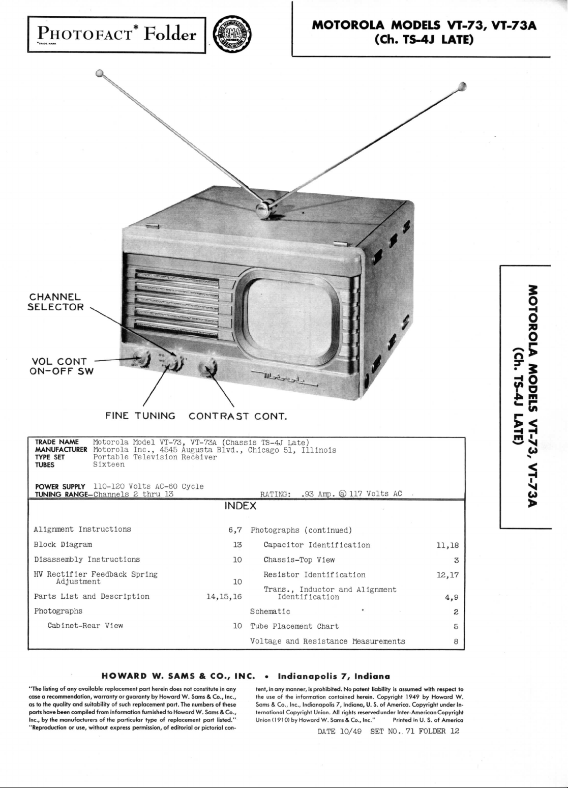
PHOTOFACT*
CHANNEL
SELECTOR
Fold
er
MOTOROLA MODELS
(Ch.
TS-4J
VT-73,
LATE)
VT-73A
I
VOL
CONT
ON-OFF
TRADE
NAME
MANUFACTURER
TYPE
SET
TUBES
Sixteen
POWER
SUPPIY
TUNING
RANGE-Channels 2 thru
Alignment
Block
Diagram
Disassembly
HV
Rectifier
Adjustment
Parts
List
Photographs
Cabinet-Rear
SW
FINE TUNING CONTRAST CONT.
Motorola
Motorola
Portable
110-120
Instructions
Instructions
Feedback
and
Description
View
Model
VT-73,
Inc.,
4545
Television
Volts
AC-60
13
Spring
VT-73A
Augusta
Receiver
Cycle
14,15,16
(Chassis
Blvd.,
TS-4J
Chicago
RATING:
Late)
51,
INDEX
6,7
Photographs (continued)
13
Capacitor
10
Chassis-Top
Resistor
10
Trans.,
Identification
Schematic
10
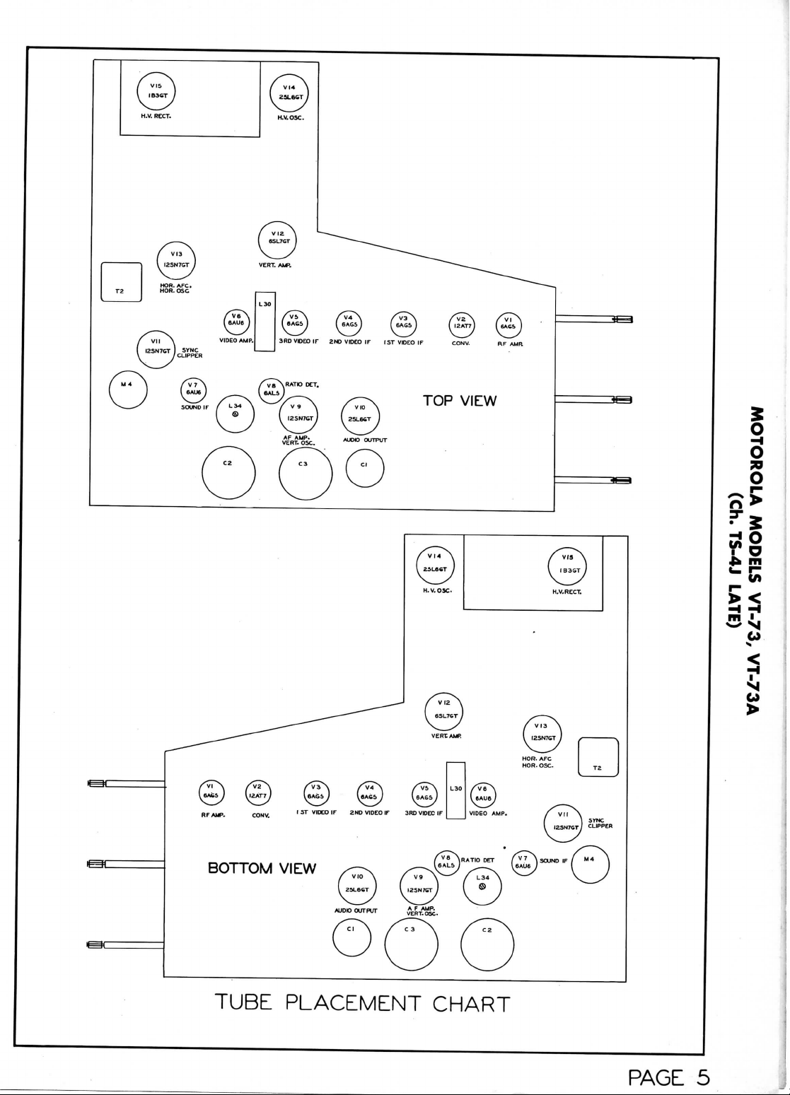
Tube Placement Chart
Voltage
and
Illinois
.95
Amp. @ 117
Volts
Identification
View
Identification
Inductor
and
Alignment
Resistance Measurements
s
5
64
AC
11,18
3
12,17
4,9
2
b
8
HOWARD
"The listing
of any
available
case a recommendation, warranty
as
to the
quality
parts
Inc.,
by the
"Reproduction
and
have been compiled
manufacturers
or
suitability
from
of the
use, without
replacement
of
information furnished
express
W.
part
or
guaranty
such
replacement
particular type
permission,
SAMS & CO., INC. • Indianapolis
tent,
in any
herein does
by
Howard
part.
to
Howard
of
replacement
of
editorial
not
constitute
W.
Sams & Co., Inc.,
The
numbers
W.
Sams & Co.,
part
or
pictorial
in any
of
these
listed."
con-
manner,
the
use of the
Sams & Co., Inc.,
ternational
Copyright Union.
Union
(1910)
by
information
Howard
7,
Indiana
is
prohibited.
No
patent
contained
Indianapolis
7,
Indiana,
All rights
W.
Sams & Co., Inc." Printed
DATE 10/49
liability
herein. Copyright
reserved
SET
is
U. S. of
America. Copyright under
under
NO..
assumed with respect
1949
by
Inter-American Copyright
in U. S. of
71
FOLDER
Howard
America
12
W.
to
In-
Page 2
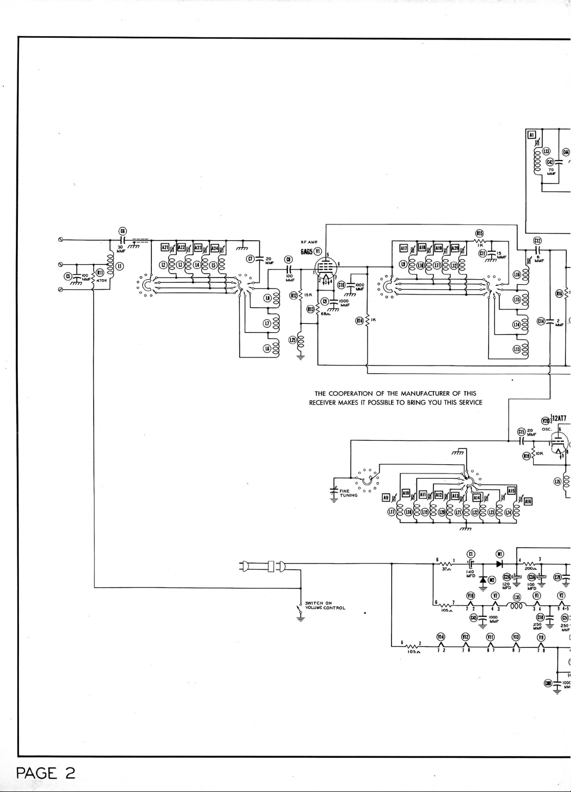
•
^^<*6&n.
I>
Z>
:>
L
.
RECEIVER
—
1000
<
®~
"""
MMF
77
THE
COOPERATION
MAKES
(JH)<
IT
>
IK
OF THE
POSSIBLE
MANUFACTURER
TO
BRING
YOU
OF
THIS
THIS
SERVICE
V-HIH-H-
® ® I 3
37-^
,,«
i
® " ® ®
. 1 A
(jg)
V-/
•±
MFD - MFD
^8
®§
^
©|
"-
^1 I 200^
©^
@^
120
-±
100
MFD ' urn
® ®
®:
I J
-i-
~
-Z*
@^
^
5
PAGE
2
Page 3
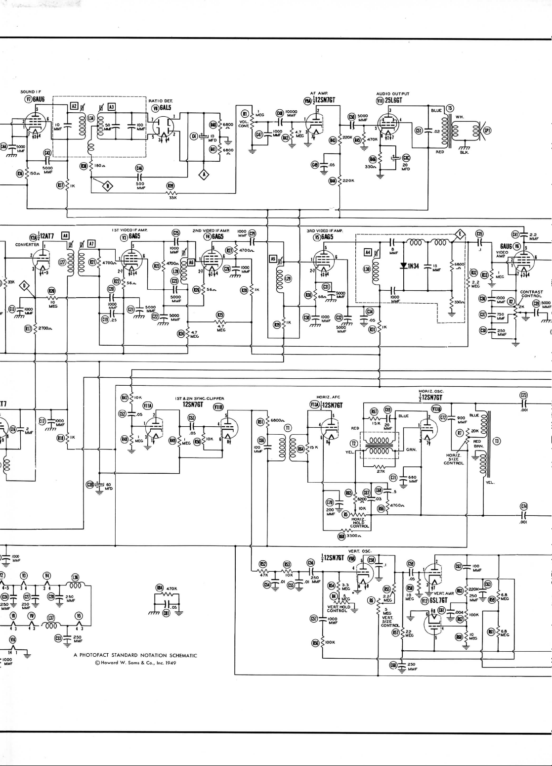
I
®6AU6
i
AUDIO OUTPUT
(ra)25L66T_
A
PHOTOFACT
STANDARD
©Howard
NOTATION
W.
Sams & Co., Inc. 1949
SCHEMATIC
Page 4
Page 5
3RD
6AS5
v_y
VDEO
I I
6AG5 ) I
v_y
If
3ND
v^x
VIDEO
IF
1ST
6AG5
VIDEO
I
IF
TOP
VIEW
I
ll2AT7J
cony.
BOTTOM
IBAG&
VIDEO
VIEW
6A&5
j
X '
IF
3RD
VIOEC
IF
TUBE PLACEMENT CHART
©
SOUND
«(
"'
v_y
}
PAGE
5
Page 6
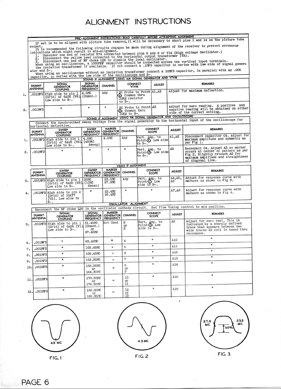
If
set is to be
socket.
It
Is
recommended
Indications
ator
capacitor,
DUMMY
ANTENNA
.001MFD
1.
2.
.001MFD
Connect
horizontal deflection.
DUMMY
ANTENNA
1.
.001MFD
2.
.001MFD
DUMMY
ANTENNA
.001MFD
3.
4.
.001MFD
Reconnect
DUMMY
ANTENNA
.OOU1FD
5.
.001MFD
6.
.OOMFD
7.
.001MFD
8.
.001MFD
9.
.001MFD
10.
.001MFD
11.
.001MFD
12.
which
1.
Unsolder
2.
Disconnect
3.
Disconnect
When
using
Use
isolation
and B-.
When
using
in
High
side
(Grid)
Low
side
the
High
side
(Grid)
Low
side
High
side
(Grid)
Low
side
High
side
(Grid)
(V2).
B-.
the RF
High
side
(Grid)
Low
side
GENERATOR
GENERATOR
ALIGNMENT
aligned
with
picture tube
the
following
might
result
the low
1
1
(V6).
1
(V3)
to
L26
1
(VI)
in
resistor
RF
choke
If
available.
without
SOUND
SIGNAL
GENERATOR
FREQUENCY
4.5M3
(Unmod.)
n
SOUND
sweep
SWEEP
GENERATOR
FREQUENCY
4.
SMC
(450KC
Sweep)
n
SWEEP
GENERATOR
FREQUENCY
251*
(10MC
Sweep)
in the
SIGNAL
GENERATOR
FREQUENCY
81.45MC
(Unmod.
or
87.45MC
93.45MC
103.45MC
109.45MC
152.35MC
158.35MC
or
164.35MC
170.35MC
or
176.35MC
182.35MC
or
189
.35MC
one end of
the
yellow lead
one end of
an
oscilloscope, a 1000HMF
transformer
an
oscilloscope
series
with
SIGNAL
COUPLING
to
pin
of
6AU6
(V6),
to B-.
"
synchronized
SWEEP
COUPLING
to
pin
of
6AU6
to
B-
.
it
SWEEP
GENERATOR
COUPLING
to
pin
of
6AG5
to
B-.
to pin 2
of
'12AT7
Low
side
choke
SIGNAL
GENERATOR
COUPLING
to
pin
'of
6AG5
to B-.
•
»
"
n
n
V
n
removed.
circuits
mis-alignment.
connected
side
IF
voltage
changes
R74
connected
to the
L26
to
disable
capacitor
If not
an
isolation
of
the
ALIGNMENT
CHANNEL
Any
IF
ALIGNMENT
from
MARKER
GENERATOR
FREQUENCY
4.5MC
MARKER
GENERATOR
FREQUENCY
23.5M3
27.
ore
22.
4M3
26.4M3
OSCILLATOR ALIGNMENT
oscillator
MARKER
GENERATOR
FREQUENCY
Not
Used
)
n
»
"
II
"
ii
ii
INSTRUCTIONS
It
will
be
necessary
be
made
during alignment
between
pins
local
be
connected
a .
and B-.
SIGNAL
GENERATOR
AD
VTVM
ADJUST
to
Point
thru
to
Point
thru
SIGNAL
generator
Vert.
Polnt<S>
to
B-.
Vert.
Point<§>
to
B-.
MMENT
Vert.
Po
int
<^
side
to-B-.
Vert.
Polnt<E>
side
to B-.
6 and 8 of V14
oscillator.
1MFD
capacitor
A1,A2
A3
GENERATOR
to the
CONNECT
SCOPE
Amp.
to
Low
Amp.
to
Low
CONNECT
SCOPE
Amp.
to
Low
n
Set
fine
CONNECT
SCOPE
Amp.
to
Low
"
«
»
n
"
II
"
horizontal output transformer
the
should
connect
transformer connect a 10MFD
oscilloscope
USING
AM
CONNECT
JC
Probe
a
Common
IOK2
resistor
to
B-.
X
Probe
a
Common
<
lOKffi
to B-.
USING
FM
the
signal
CHANNEL
Any
n
VII
EO
IF
ALIG
CHANNEL
Any
cathode
circuit.
CHANNEL
2
or
3
4
5
6
7
8
or
9
10
or
11
12
or
13
to
short
of the
(High
across
the
In
capacitor,
AND
VTVM
HIST
Adjust
Adjust
negative
side
AND
OSCILLOSCOPE
horizontal
ADJUST
A1,A2
side
A3
side
ADJUST
A4,A5,
A6
A7,A8
tuning control
ADJUST
A9
A10
All
A12
A13
A14-
A15
A16
pins
1 and 14 on the
receiver
voltage
(T3).
vertical
series
for
for
reading
of the
Disconnect
maximum
per
Reconnect
occurs
Fig
maximum
of
Adjust
markers
Adjust
markers
Adjust
Indicated
trace
wide
resonance.
to
prevent erroneous
Oscillator.)
input
with
maximum
zero reading. A positive
correct
Input
Fig
2.
diagonal
to mid
traces
terminals.
low
side
in
parallel
REMARKS
deflection.
will
be
setting.
of the
capacitor
amplitude
1.
C4.
Adjust
at
center
Slightly
amplitude
line.
for
response curve
as
shown
for
response
as
shown
position.
for
zero
by a
that
appears
as
"
"
"
n
"
n
11
picture tube
of
signal
genera
with
an
.005
obtained
oscilloscope
REMARKS
and
of
pattern
retouch
and
REMARKS
In
Fig 3.
in Fig 4.
REMARKS
beat.
sharply defined
between
coil
is
and
on
for
C4.
Adjust
symmetry
A3 so
marker
as per
A2 for
straightness
with
curve
with
This
is
two
tuned
either
for
as
thru
PAGE
6
FIG.
FIG.
I
FIG.2
3
Page 7
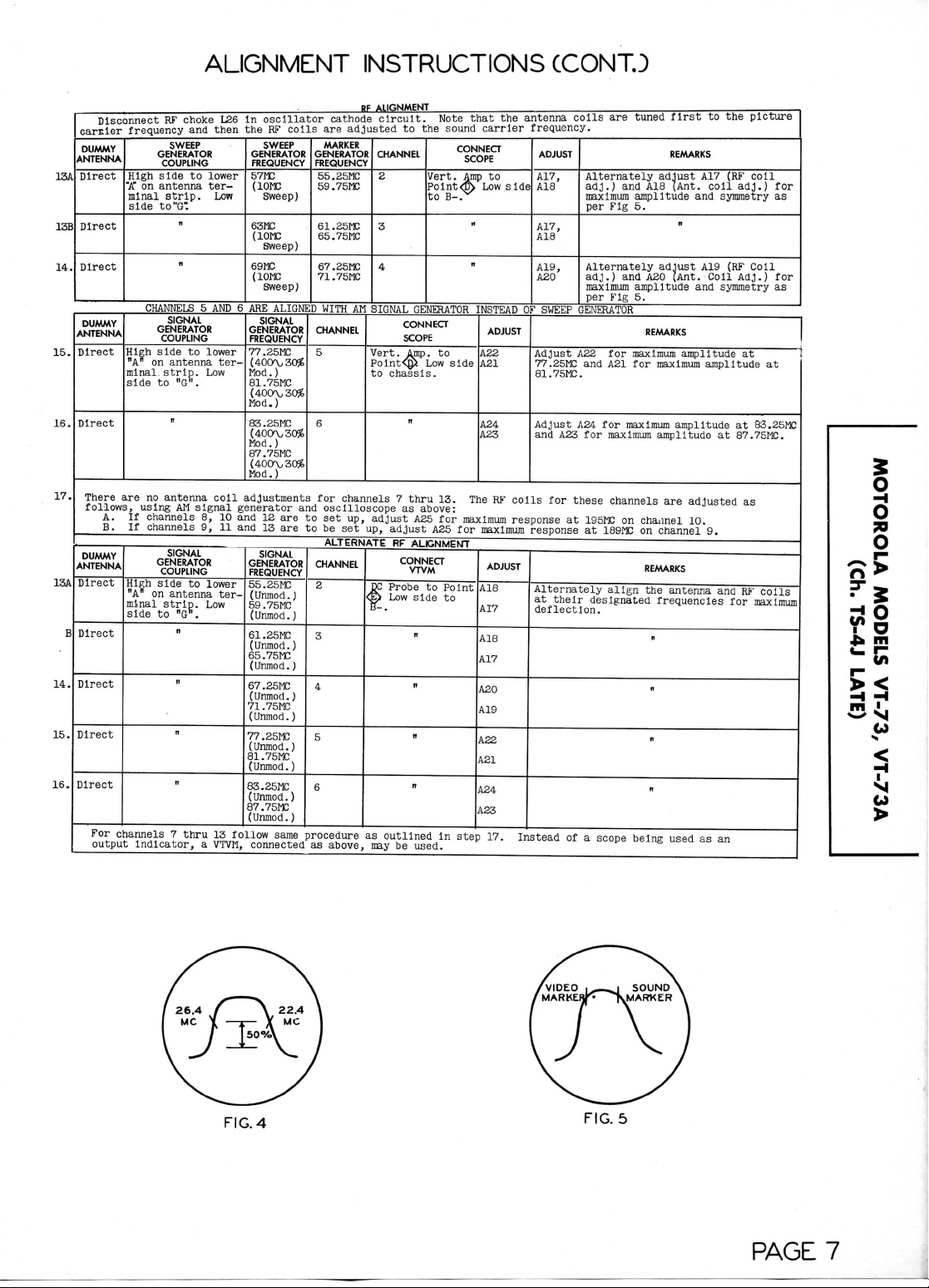
"
Disconnect W choke
careler
frequency
DUMMY
ANTENNA
High
Direct
ISA
13B
14.
15.
16.
17.
ISA
B
14.
15.
16.
Direct
Direct
DUMMY
ANTENNA
Direct
Direct
There
are no
follows,
A.
If
B.
If
DUMMY
ANTENNA
Direct
Direct
Direct
Direct
Direct
For
channels 7 thru
output
"A"
on
minal
side
High
"A"
minal,
side
using
channels
channels
High
"A"
minal
side
indicator, a VTVM,
ALIGNMENT INSTRUCTIONS CCONTJ
L26
ana
then
SWEEP
GENERATOR
COUPLING
side
to
lower
antenna
ter-
strip.
Low
to"G".
11
n
CHANNELS 5 AND
SIGNAL
GENERATOR
COUPLING
side
to
on
on
lower
antenna
ter-
strip.
Low
to
"G".
n
antenna
coil
AM
signal
8, 10 and
9, 11 and 13 are to be set up,
SIGNAL
GENERATOR
COUPLING
side
to
lower
antenna
"G".
n
Low
ter-
strip.
to
13
in
oscillator
the
RF
coils
SWEEP
GENERATOR
FREQUENCY
57M3
done
Sweep)
63MC
(10M3
Sweep)
69MC
(1OTE
Sweep)
ARE
ALIGNED
6
SIGNAL
GENERATOR
FREQUENCY
77.25MC
(400%
3056
Mod.)
81.75MC
(400%
3056
Mod.)
83.25MC
(400%
Mod.)
87.75MC
(400% 3054
Mod.)
adjustments
generator
12
are to set up,
SIGNAL
GENERATOR
FREQUENCY
55.25MC
(Unmod.)
59.75MC
(Unmod.)
61.25MC
(Unmod.)
65.75MC
(Unmod.)
67.25M3
(Unmod.)
71.75MC
(
Unmod . )
77.35MC
(Unmod.)
81.75MC
(Unmod.)
83.25MC
(Unmod.)
87.75MC
(Unmod.)
follow
same
connected
GENERATOR
FREQUENCY
3056
for
and
procedure
as
OF
ALIGNMENT
cathode
are
MARKER
55.25MC
59.75M3
61.25M3
65.75MC
67.25M3
71.75MC
WITH
CHANNEL
5
6
CHANNEL
circuit.
adjusted
CHANNEL
2
3
AM
SIGNAL
Vert . Amp . to
Polnt<g>.
to
channels 7 thru
oscilloscope
adjust
ALTERNATE
2
f
3
4
5
6
as
above,
may be
,
Note
that
the
antenna
coils
are
tunea
«rst
u,
mo
A17 (RF
coll
adj.)
symmetry
A19 (RF
Adj.)
symmetry
amplitude
at
at
87.75MC.
9.
and RF
for
as an
v^^»
coll
Coil
at
at
83.25MC
as
coils
maximum
for
as
for
as
to the
4
GENERATOR
CONNECT
SCOPE
Low
chassis.
as
A25 for
adjust
RF
ALIGNMENT
CONNECT
VTVM
Probe
Low
side
w
outlined
used.
sound
CONNECT
SCOPE
Vert.
Amp
Point
<JJ>
to
B-X
rt
INSTEAD
side
13. The RF
above:
maximum
A25 for
to
Point
to
in
step
carrier
to
Low
side
ADJUST
A22
A21
A24
A23
colls
response
maximum
ADJUST
A18
AI7
A18
A17
A20
A19
A22
A21
A24
A23
17.
Instead
frequency.
ADJUST
A17,
A18
A17,
A18
A19,
A20
1
SWEEP
0
Adjust
A22 for
77.25MC
81.75MC.
Adjust
A24 for
and
A23 for
for
these channels
at
response
Alternately
at
their
deflection.
of a
REMARKS
Alternately
adj.)
maximum
per
Alternately adjust
adj.)
maximum
per
GENERATOR
and A21 for
maximum
195M3
at
189MC
designated frequencies
scope
and A18
amplitude
Fig 5.
and A20
amplitude
Fig 5.
REMARKS
maximum
maximum
maximum
on
channel
on
REMARKS
align
the
being used
adjust
(Ant.
and
(Ant. Coll
and
amplitude
amplitude
amplitude
are
adjusted
10.
channel
antenna
n
n
n
n
I
5
73
o
FIG.4
FIG.
5
PAGE?
Page 8

MEASUREMENTS
RESISTANCE
AND
9
Pin
242
8
Pin
2.5ffl
ia
3302
222
222
fioooa
TOP CAP
12
172
Inf.
1002
Inf.
1
7
Pin
esa
lOKffi
6
Pin
T10002
ifl.2K2
5
Pin
tioooa
21.52
4
Pin
242
READINGS
RESISTANCE
21.52
3
Pin
262
2.7K2
2
Pin
68S2
33K2
1
Pin
ftOOOffl
15Ka
Tub«
6AG5
1SAT7
2
1
Item
V
V
9
Pin
48VAC
8
Pin
.1VDC
7
Pin
.5VDC
S-.2VDC
6
Pin
90VDC
220VDC
tioooa
562
Inf.
ft. 2Ka
Inf.
I1.2K2
#5.5K2
inf.
ifl.2K2
169
192
122
21.52
192
152
Inf.
T10002
562
Meg.
T10002
2
4.7 Meg
6AG5
6AG5
6AG5
V3
V4
V 5V6
.6VDC
T13VDC
120VDC
T125VDC
225VDC
120VDC
Meg.
T1502
1
2K2
iH.SKffi
#11.5K2
72
11.5SZ
2KS2
Meg.
1
6AU6
5.2VDC
250VDC
112
422
172
252
112
#1.2K2
470Ka
Meg.
#1.2K2
1
302
12
27S
?ffi
T1502
6.8K2
8KB
T12
6.
6AU6
6AL5
8
7
V
V
T1.4VDC
4.6VDC
.1VDC
T135VDC
T02
oa
Inf.
02
3.3K2
7K2
Ilifiif
Mee
8.3 Meg
3.3
02
if440K2
Meg.
5
12SN7GT
V9
VAC
3
6.
20VAC
OV
inf.
t
470K2
toa
T240a
302
Inf.
25L6GT
10
V
8.6VDC
87VAC
OV
18K2
Meg.
TlOKa
10
18K2
8.2K2
oa
02
2002
1 Meg
T
Inf.
#20K2
15002
Meg.
Meg.
1
10
18K2
8.2Kfi
12SN7GT
6SL7GT
12SN7GT
13
12
V
Vll
V
50VAC
50VAC
35VAC
56VAC
35VAC
20VAC
tov
OV
17VDC
14
V
382
Offi
150Ka
#3002
#3002
252
Inf.
25L6GT
3.5VDC
85VAC
OV
10 j 11 14
Inf.
Inf.
9
Inf.
678
Inf.
5
4
Inf.
Inf.
23
1
Inf.
1B3GT
15
PINS
V
14
10 11
9
8
7
#700K2
Inf.
Inf. Inf.
Inf.
Inf
02
450K2
02
7JP4
¥16
6.3VAC
«
*
«
*
#
volt-
Ml,
Vll.
Of
Output
Pin 6 Of
From
From
Measured
Measured
T
#
to the
for
volts
117
at
maintained
voltage
reodings.
Line
age
4.
1,000
20,000
at
are at
measured
Voltage
AC
measurements
volt;
per
Voltage
ohms
1. DC
us.
urn
ohms.
according
minimum.
vary
set at
may
controls
readings
panels
Front
WKere
6.
5.
direc-
j-
-
clockwise
a
i i
in
•
socket.
counted
of
are
j
bottom
on
numbers
,
tion
Pin
.
..
_
2.
minimum
both
given.
are
controls,
readings
service
of the
maximum
setting
and
com-
pin to
stated.
socket
from
otherwise
ore
unless
values
negative
mon
Measured
3.
VOLTAGE
m
co
T82VDC
270VDC
t-.5VDC
-1.2VDC
OV
OV
13.5VDO»155VDC
9VDC
.
-1.8VDC
-1
12SN7GT
6SL7GT
1
12
1
V
V
DC
-57VDC
-52V
OV
-57VDC
-52VDC
245VDC
9VDC
.
1
245VDC
56VAC
345VDC
0V
-43.5VDC1
-47.5VDCI
12SN7GT
25L6GT
13
14V 15
V
V
6
415
3
2
0V
MEASfJRE.
* DO HOT
1B3GT
1
PINS
_|
*
..1.
0V
225VDC
Vll.
Pin 6 Of
0V
From
7JP4
Measure.
6
Do Wot
Measured
VI
T
*
5
Pin
90VDO
40VAC
80VDC
187VDC
4
Pin
48VAC
READINGS
3
Pin
VOLTAGE
54VAC
2
Pin
.5VDC
1
Pin
-.1VDC
Tube
6AG5
Item
V 1
40VAC
34VAC
8VDC
40VAC
.6VDC
0V
.1VBC
220VDC
12AT7
6AG5
V 2V 3V4
27VAC
34VAC
120VDC
77VDC
6AG5
T135VDC
T135VDC
230VDC
OV
14VDC
OV
45VDC
DC
.TV
.7VDC
60VAC
6.3VAC
13VAC
20VAC
27VAC
20VAC
54VAC
T1.4VDC
T13VDC
5.2VDC
0V
T
T11.5VDC
0V
6AU6
6AG5
6AU6
6
V7
V5
V
100VDC
DC
13VAC
ov
93V
-3.6VDC
18VDC
60VAC
11VDC
-.5VDC
0V
6AL5
12SK7GT
25L6GT
8
10
V9
V
V
Page 9

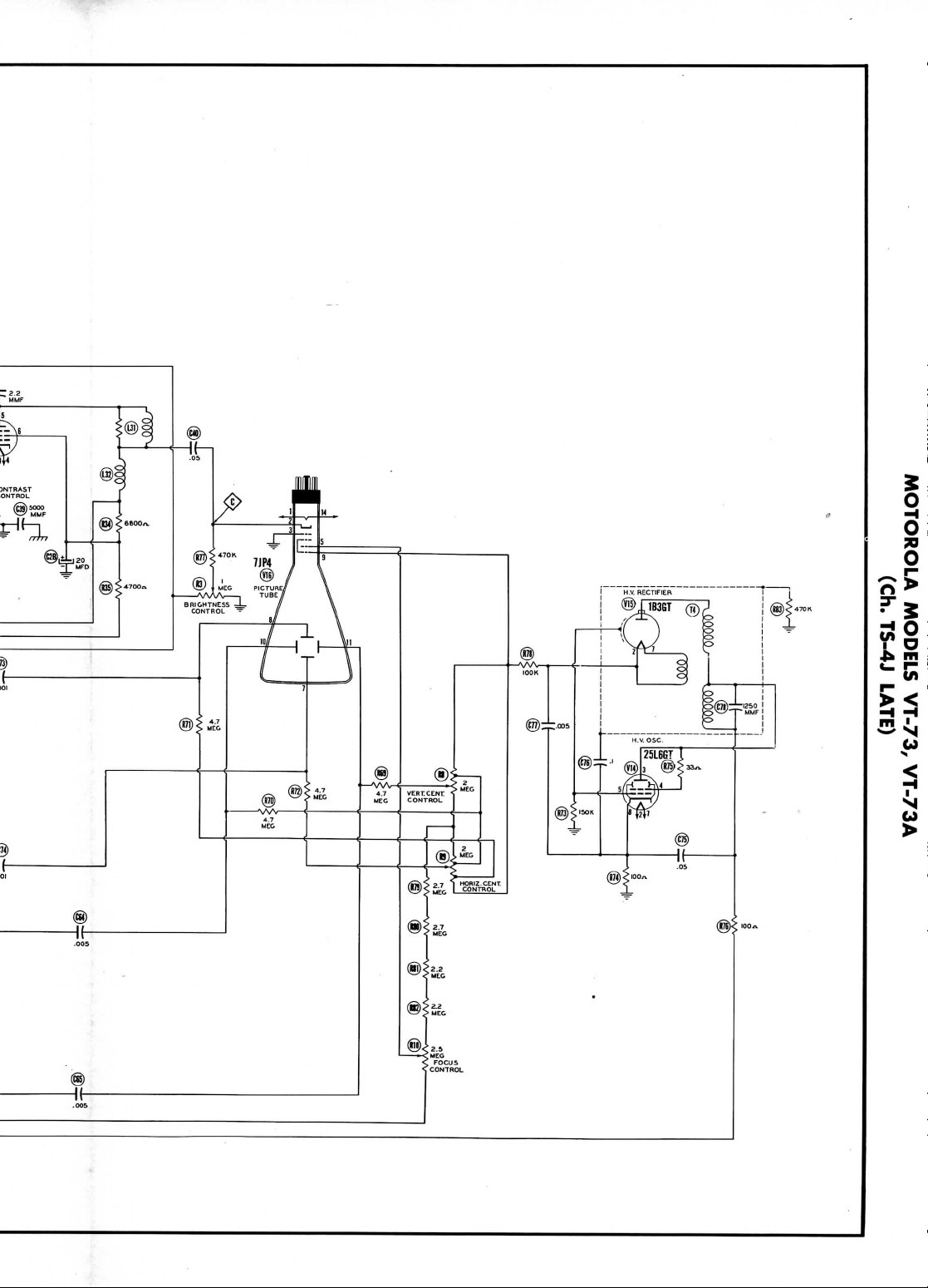
VT-73A
>
UJ
Q_
COCOCO
<
CJ
VT-73,
MODELS
MOTOROLA
LATE)
(Ch. TS-4J
Page 10

FOCUS
HORIZ.
CENT.
VERT. WIDTH
HEIGHT
HORIZ.
VERT. BRIGHTNESS
CENT. CONT. CONT. HOLD HOLD
1.
Remove 6 screws
2.
Remove
3.
Unplug speaker leads.
4.
Remove picture tube socket.
5.
Remove 4 chassis bolts from bottom
6.
Slide
7.
Remove 4 nuts
POSITIONING
Feedback
to the
consisting
tion
age.
of
this
Two
bottom edge
of a
coll mounted
spring
CABINET-REAR
DISASSEMBLY
holding
back
panel
push
on
type knobs
chassis
out
and
OF
FEEDBACK
grid
of H. V.
around
is
very critical
of the
spring should
and 2
rear
of
cab.
lock
washers
Oscillator tube
the
envelope
and
misplacement will
be
VIEW
INSTRUCTIONS
and
power
felt
washers
of
cabinet.
on
speaker
SPRING
Is
obtained
of the
3/4" ± 1/32"
interlock
on
and
remove.
High Voltage rectifier
,-esult
from
and
front
of
receiver.
ON KV.
by a
capacltive coupling
In
very
the top of the
remove.
low or no
tube
RECTIFIER
device
tube.
The
posi-
high
volt-
base.
PAGE
10
Page 11

VT-13
MOTOROLA
vioaoiow
DIAGRAM
siaaow
(31V1
BLOCK
'ez-iA
ve/-iA
IF V3
IF V4
IF V5
VIDEO
VIDEO
VIDEO
1st
2nd
3rd
VI
V2
AMP.
CONV.
RF
m
o
03
Page 12

ITEM
No.
VI
V2
V3
V4
V5
V6
V7
V8
V9
V10
VII
V12
VIS
V14
V15
V16
ITEM
01
C2A
C3A
C4
C5
06
C7
C8
C9
CIO
Oil
C12
C13
C14
C15
C16
017
CIS
019
020
021
022
023
024
025
C26
C27
C28
029
030
031
C32
C33
C34
035
036
037
038
C39
C40
041
042
C43
044
C45
046
047
C48
C49
050
051
C52
053
C54
C55
C56
C57
C58
059
060
061
062
063
C64
065
066
C67
C68
C69
No.
KF
Amp.
Converter
1st
2nd
3rd
Video
Sound
Ratio
AF
Amp.
Osc.
Audio
1st &
Clipper
Vert.
Hor.
Osc.
HV
Osc.
HV
Rectifier
Picture
CAP.
140
120
B
20
100
B
60
C
20
10
100
30
20
100
1000
1000
15
3
1000
£
20
2
1000
250
.25
1000
5000
5000
5000
250
1000
1000
250
250
1000
1000
5000
5000
250
.05
.1
1000
750
250
5000
.05
2.2
70
5000
5000
1000
500
1000
10000
.05
5000
.02
.05
.05
.01
.01
250
1000
.1
.05
250
.004
100
250
.005
.005
100
.03
.5
20
USE
Video
IF
Video
Video
IF
Amp.
IF
Det.
-Vert.
Output
2nd
Sync.
Amp.
AFC-Hor.
Tube
RATING
VOLT
150
300
300
300
150
25
50
300
200
600
100
600
500
600
600
600
600
600
600
500
600
600
600
6000
6000
600
200
Amp.
IF
Amp.
Amp.
MOTOROLA
23B48097
23B90134
23B90136
23A90205
21R6631
21K470329
21K470322
21B77286
21K478410
21K478410
21K470323
21K470324
21K478410
21K478280
21K478287
21K478280
21K478410
21R6648
8A471356
21K478410
21A470789
21A470789
21A470789
21R6648
21K478410
21K478410
21R6648
21R6648
21K478410
21K478410
21A470789
21A470789
21R6648
8A471151
8A471366
21K780599
21K780598
21K77375
21A470789
8A471151
21A478274
21K470328
21A470789
21A470789
21K478410
21R6590
21K478410
21K482726
8A471151
21A470789
8A471152
8A471151
8A471151
8A471153
8A471153
21R6648
21R6630
8A471149
8A471151
21A481402
8A471156
21A471211
21R6648
8K484866
8K484866
21R6631
8A482184
8A484814
21K470322
MOTOROLA
PART
6AG5
12AT7
6A05
6AG5
6AG5
6AU6
6AU6
6AL5
12SN70T
25L6GT
12SN7GT
6SL7GT
12SN7GT
25LSGT
1B3GT
7JP4
Capacity
and
Paper
PART
No.
TUBES
REPLACEMENT
No.
values
given
Capacitors,
AEROVOX
PART
AFH28D
AFH244G
AFH20G12D4A
PRS50/10
1468-0001
1468-00004
1468-0001
1468-001
1468-001
1468-001
1468-001
1468-00025
P488-25
1468-001
1467-005
1467-005
1467-005
1468-00025
1468-001
1468-001
1468-00025
1468-00025
1468-001
1468-001
1467-005
1467-005
1468-00025
P688-05
P288-1
1468-001
1468-00075
1468-00025
1467-005
P688-05
1467-005
1467-005
1468-001
1468-0005
1468*001
P488-01
P688-05
1467-005
P688-02
P688-05
P688-05
P688-01
P688-01
1468-00025
1468-001
P688-1
P688-05
1468-00025
P688-004
1468-0001
1468-00025
7584-005
7584-005
1469-0001
P688-03
P288-5
(SYLVANIA
DATA
STANDARD
REPLACEMENT
6AG5
12AT7
6AG5
6AGS
6AG5
6AU6
6AU6
6AL5
12SN7GT
85L6GT
12SN7GT
6SL7GT
12SN7GT
35L6GT
1B3GT
7JP4
CAPACITORS
in the
rating
and in
REPLACEMENT
No.
mmfd.
DATA
CORNELL-
DUBILIER
PART
No.
UP6AJ333
UP9BJ993
UP9CJ994
BR105
5W5T1
5W553
5R5Q2
5W5T1
1W5D1
1W5D1
1W5D1
5W5Q2
1W5D1
5W5T25
GT2P25
1W5D1
1D5D5
1D5D5
1D5D5
5W5T25
1W5D1
1WSD1
5W5T25
5W5T25
1W5D1
1W5D1
1D5D5
1D5D5
5W5T25
GT6S5
GT2P1
1W5D1
1W5T8
5W5T25
1D5D5
GT6S5
5R5Q7
1D5D5
1D5D5
1W5D1
5W5T5
1W5D1
GT4S1
GT6S5
1D5D5
GT6S2
GT6S5
GT6S5
GT6S1
GT6S1
5W5T25
1W5D1
GT6P1
GT6S5
5W5T25
GT6D4
5W5T1
5W5T25
DSTH60D5
DSTH60D5
5R5T1
GT6S3
GT2P5
5W5Q2
.
7BD
9A
7BD
7BD
7BD
7BK
•7BK
6BT
8BD
7AC
8BD
BED
8BD
VAC
3C
column
or
Equivalent)
RMA
BASE
TYPE
are in
for
Mica
ERIE
PART
No.
GP1K-100
GP1K-33
NPOK-20
GP1K-100
GP2L-001
GP2L-001
OP1K-1S
GP2L-001
NPOK-20
GP2L-001
GP2K-250
GP2L-001
811-005
811-005
811-005
GP2K-250
GP2L-001
GP2L-001
GP2K-250
GP2K-250
QP2L-001
GP2L-001
811-005
811-005
GP2K-250
GP2L-001
GP2K-750
GP2K-250
811-005
811-005
811-005
GP2L-001
GP2K-500
GP2L-001
821-01
811-005
3P2-335-01
GP2-335-01
3P2K-250
3P2L-001
GP2K-250
GP1K-100
GP2K-250
NPOM-100
NPOK-50
and
mfd.
for
Ceramic
SPRAGUE
PART
No.
D6282
TVL-46
TVL-51
TVA-14
1FM-31
ffi-43
MS-42
1FM-31
1FM-21
1FM-21
MS
-415
1FM-21
MS-42
1FM-21
1FM-325
rTO-2
1FM-21
29C1
29C1
2901
LFM-325
1FM-21
1FM-21
LFM-325
LFM-325
1FM-21
1FM-21
29C1
29C1
LFM-325
TM-15
TM-1
1FM-21
1FM-37
LFM-325
2901
TM-15
MS-47
29C1
29C1
1FM-21
1FM-35
1FM-21
36C1
TM-15
29C1
TM-12
TM-15
TM-15
TM-11
TM-11
1FM-325
1FM-21
TM-1
TM-15
1FM-325
TM-24
1FM-31
1FM-325
TVM-25f
TVM-256
M3-31
TM-13
TC-5
MS-42
NOTES
Electrolytic
Capacitors.
IDENTIFICATION
INSTALLATION
m
Doubler
A
o
A
Stabilizing
Ext.
Ant.
Fixed
RF
RF
RF
RF
Mixer
Osc.
Osc.
Osc.
Decoupling
RF
AGC
RF
1st V. IF
1st V. IF
1st V. IF
2nd V. IF
2nd
3rd V. IF
3rd V. IF
3rd V. IF
3rd V. IF
3rd V. IF
Video
V.
n
RF
Video
S.
Fixed
S. IF
S. IF
S.
Diode
De-emphasis
Audio
AF
Audio
Output
Sync.
Cap.
Filter
Video
Amp.
Filter
Filter
Output
Cath.
Ground
Coupling
Trimmer
Coupling
Cath.
Bypass
Decoupling
n
n
Coupling
Cath.
Coupling
Grid
Cap.
Feedback
Fil.
Bypass
Filter
Bypass
Decoupling
Grid
IF
IF
ii
Fll.
Coupling
Decoupling
V. IF
Fil.
Coupling
Decoupling
Cath.
Decoupling
Fll.
Decoupling
Coupling
Amp.
Cath.
n n
Bypass
Coupling
IF
Coupling
Trimmer
Decoupling
Cath.
IF
Fil.
Load
Coupling
Plate
Decoupling
Coupling
Plate
Coupling
n
ti
Integrator
Vert.
Sync.
Vert.
Feedback
Vert.
Discharge
Vert.
Sweep
Linearity
Voltage
Vert.
Fixed
Hor.
Hor.
Comp.
Divider
Sweep
Trimmer
Osc.
Feedback
AND
NOTES
Dec.
Bypass
Cap.
Isolation
Bypass
Dec.
Byp.
Bypass
Bypass
Bypass
Bypass
Bypass
Bypass
Cap.
Bypass
Net.
.
Coupling
Coupling
Coupling
Grid
Cap.
CODES
*
ITEM
No.
C70
C71
C7g
C73
C74
C75
C76
C77
C78
C79
C80
C81
» Not
ITEM
No.
R1A
B
C
R2
R3
R4
R5
R6
R7
R8A
B
R9A
B
R10A
B
#
Use
* Use
required.
inserted
ITEM
No.
Rll
R12
R13
R14
R15
R16
R17
R18
R19
R20
R21
R22
R23
R24
R25
R26
R27
R28
R29
R30
R31
R32
R33
R34
R35
R36
R37
R38
R39
R40
R41
R42
R43
R44
R45
R46
R47
R48
R49
R50
R51
R52
R53
R54
R55
R56
R57
R58
R59
R60
R61
R62
R63
R64
R65
R66
R67
R68
RATING
CAP.
200
680
900
.001
.001
.05
.1
.005
1250
1000
1000
.05
used
RATING
RESIST-
ANCE
1
Meg.
Shaft
Switch
20002
1
Meg.
5
Meg.
10K2
5
Meg.
20K2
2
Meg.
Shaft
2
Meg.
Shaft
2.5 Meg
Shaft
original
original
into
RESISTANCE
470K2
15K2
682
10002
10002
33K2
27002
10002
10K2
10
Meg.
47002
562
47002
4.7
Meg.
4.7
Meg.
562
47002
10002
10002
682
10002
2.2
Meg.
1
Meg.
68002
47002
1502
10002
1802
33K2
68002
68002
4.7
Meg.
220K2
220K2
470K2
3302
10K2
1
Meg.
1
Meg.
10K2
68002
47K2
10K2
3.3
Meg.
2.2
Meg.
100K2
22
Meg.
10
Meg.
6.8
Meg.
10
Meg.
6.8
Meg.
100K2
220K2
15K2
82002
47002
15K2
33002
VOLT
500
2000
2000
6000
6000
600
200
6000
500
600
In
WATTS
Lock
RATING
PARTS
MOTOROLA
PART
21R662S
21R2741
21R2739
8A480255
8A4802S5
8A471151
8A471355
8A471348
21R2738
21K478410
21K478410
8A471151
all
MOTOROLA
18A90142
4
Not
Not
4
18A780359
18A90147
I
18A90145
4
18A780098
4
18A90145
£
18A90144
£
18A478285
Not
18A478286
4
Not
18A90148
4
Not
insulated
insulated
ring
slot.
WATTS
4
4
4
4
X
X
X
i
4
4
4
4
4
X
4
I
4
4
2
2
4
4
4
4
4
X
4
4
4
•^
I
H
i
£
1
X
X
X
X
I
4
^
1
4
1
4
4
4
1
4
4
4
No.
models.
PART
No.
Req.
Req.
Req.
Req.
Req,
spacer
spacer
should
MOTOROLA
PART
6R6377
6R6477
6R2039
6R62S9
6R6229
6R6410
6R5577
6R6229
6R63SO
6R2109
6R6080
6R5614
6R6080
6R6446
6R6446
6R5614
6R6080
6R6229
6R6229
6R2039
6R6229
6R6433
6R6046
6R5690
6R5671
6R6229
6R5660
6R6410
6R6428
6R6428
6R6446
6R6407
6R6407
6R6377
6R6022
6R6320
6R6046
6R6046
6R6320
6R5691
6R6048
6R6320
6R6497
6H6433
6R6031
6R488252
6R5622
6R488157
6RS622
6R488157
6R6031
6R6407
6R6477
6R5610
6R6030
6R6477
6R5581
LIST
CAPACITORS
AEROVOX
PART
No.
1468-0002
7584-001
7584-001
P688-05
P288-1
7584-005
1468-001
1468-001
P688-05
REPLACEMENT
IRC
PART
513-137
Not
Req.
76-1
Qll-137
411-141
Qll-116
Qll-141
Q18-139X
RQ
t
Q13-139XX
RQ f
Qll-239
RQ
if
bushing
bushing
be
removed
REPLACEMENT
No.
BTS-470K
BTS-1000
BTS-1000
BTS-33K
BTS-4700
BTS-4700
BTS-4.7
BTS-4.7
BTS-4700
BTS-1000
BTS-1000
BTS-1000
BTS-2.2
BTS-1
BT-2-6800
BT-2-4700
BTS-1000
BTS-33K
BTS-6800
BTS-6800
BTS-4.7
BTS-220K
BTS-220K
BTS-470K
BW-4-330
BTS-10K
BTS-1 Meg.
BTS-1 Meg.
BTS-10K
BTA-6800
BTS-47K
BTS-10K
BTS-3.3
BTS-2.2
BTS-100K
BTS-22
BTS-10
BTA-6.8
BTS-10 Meg.
BTA-6.8
BTS-100K
BTS-220K
BTS-15K
BTA-8200
BTS-4700
BTS-15K
BTS-3300
AMI
REPLACEMENT
CORNELI
DUBILIE!
PART
5W5T2
DSTH60I
DSTH60r
GT6S5
GT2P1
DSTH60I
1W5D1
1W5D1
GT6S5
CON
DATA
CLARO
No.
PART
AM-63-
KSS-3
SW-A
M-61-E
M-8S-E
M-27-E
M-85-E
AT-llf
and E
and £
from
RESI
DATA
IRC
PART
No.
Meg
Meg
Meg
Meg.
Meg
Mef
Mef
Meg.
Meg.
Mej
Me(
•
PAGE
14
Page 13

lettrolytic
apacitors.
IDENTIFICATION CODES
AND
INSTALLATION NOTES
Doubler
Cap.
•
Filter
Video Amp.
.
Filter
:
Filter
.
Output
tabllizing
;xt.
.nt.
ixed
:F
Coupling
,F
Cath.
;F
Decoupling
;F
Coupling
llxer
)sc.
)sc.
)sc.
lecoupllng
(F
Fll.
J3C
Filter
IF
Bypass
.st
1st
V. IF
1st
V. IF
[F
Coupling
2nd
V. IF
ind
V. IF
IF
Coupling
5rd
V. IF
5rd
V. IF
5rd
V. IF
5rd
V. IF
5rd
V. IF
/idso
/.
Amp.
W
Bypass
/ideo
3. IF
?lxed
3. IF
3.
IF
3.
IF
Diode
De-emphasis
Audio
AF
Plate
Audio
Output
Sync.
Integrator
Vert.
Vert.
Vert.
Vert.
Linearity
Voltage
Vert.
Fixed
Hor.
Hor.
Dec.
Cath.
Cap.
Ground
Isolation
Coupling
Trimmer
Bypass
p
Cath. Bypass
Coupling
Grid
Cap.
Feedback
Bypass
V. IF
Decoupling
Grid
Fil.
Decoupling
Fil.
Decoupling
Cath.
Decoupling
Fil.
Decoupling
Coupling
Cath. Bypass
Coupling
Coupling
Trimmer
Decoupling
Cath. Bypass
Fll. Bypass
Load
Cap.
Coupling
Decoupling
Coupling
Plate
Bypass
Coupling
Net.
Sync.
Coupling
Feedback
Discharge
Sweep
Coupling
Comp.
Divider
Sweep
Coupling
Trimmer
Osc.
Grid
Feedback
Bypass
Dec.
Byp.
Bypass
Bypass
Bypass
Cap.
PARTS
RATING
ITEM
CAP.
No.
200
C70
C71
680
C7S
900
.001
C73
.001
074
.05
C75
.1
C76
C77
.005
C78
1250
1000
C79
C80
1000
C81
.05
* Not
ITEM
No.
RESIST-
ANCE
1
Meg.
R1A
Shaft
B
Switch
C
R2
20002
1
Meg.
R3
5
Meg.
R4
lOKffi
R5
5
Meg.
R6
R7
20K2
2
Meg.
R8A
B
Shaft
R9A
Z
Meg.
Shaft
B
R10A
2.5 Meg
Shaft
B
Use
original
* Use
original Insulated spacer bushing
required. Lock
inserted
ITEM
No.
RESISTANCE
470K2
Rll
R12
15K2
R13
682
R14
1000S!
R15
10002
R16
33K2
R17
27002
R18
10002
R19
10K2
10
Meg.
R20
R21
47002
R22
562
4700B
R23
4.7
R24
4.7
R25
R26
56ffl
R27
47002
R28
10002
R29
10002
R30
R31
R32
R33
R34
R35
R36
R37
R38
R39
R40
R41
R42
R43
R44
R45
R46
R47
R48
R49
R50
R51
R52
R53
R54
R55
R56
R57
R58
R59
R60
R61
R62
R63
R64
R65
R66
R67
R68
682
10002
2.2
1
Meg.
68002
47002
1502
10002
1802
33K2
68002
68002
4.7
220K2
220K2
470K2
3302
10K2
1
Meg.
1
Meg.
10K2
68002
47K2
10K2
3.3
2.2
100K2
22
Meg.
10
Meg.
6.8
10
Meg.
6.8
100K2
220K2
15K2
82002
47002
15K2
33002
*
MOTOROLA
VOLT
PART
500
2000
2000
6000
6000
600
200
6000
500
600
used
RATING
into
RATING
Meg.
Meg.
Meg.
Meg.
in all
WATTS
No.
21R6629
31R2741
21R2739
8A480255
8A480255
8A471151
8A471355
8A471348
21R2738
81K478410
21K478410
8A471151
models.
MOTOROLA
PART
18A90142
4
Not
Not
1
18A780359
I
18A90147
1
18A90145
1
18A780098
18A90145
4
18A90144
jjj
18A478285
Not
18A478286
4
Not
18A90148
4
Not
Insulated spacer bushing
ring
slot.
WATTS
4
^
I
^
I
£
4
4
4
•£
£
4
£
2
2
JT
I
I
I
i
^
I
1
Meg.
Meg.
Meg.
Meg.
4
1
4
1
i
1
4
i
X
X
4
No.
Req.
Req.
Req.
Req.
Req.
should
REPLACEMENT
MOTOROLA
PART
6R6377
6R6477
6R2039
6R6229
6R6229
6R6410
6R5577
6R6229
6R6320
6R2109
6R6080
6R5614
6R6080
6R6446
6R6446
6R5614
6R6080
6R6229
6R6229
6R2039
6R6229
6R6433
6R6046
6RS690
6R5671
6R6229
6R5660
6R6410
6R6428
6R6428
6R6446
6R6407
6R6407
6R6377
6R6022
6R6320
6R6046
6R6046
6R6320
6R5691
6R6048
6R6320
6R6497
6X6433
6R6031
6R488252
6RS622
6R488157
6R5622
6R488157
6R6031
6R6407
6R6477
6R5610
6R6080
6R6477
6R5581
LIST
AEROVOX
1468-0002
7584-001
7584-001
P688-05
P288-1
7584-005
1468-001
1468-001
P688-05
AND
CAPACITORS
REPLACEMENT
No.
CORNELLPART
SW5T2
DSTH60D1
DSTH60D1
GT6S5
GT2P1
DSTH60D5
1W5D1
1W5D1
GT6S5
PART
DUBILIER
CONTROLS
REPLACEMENT
be
No.
'
DATA
IRC
PART
No.
Q13-137
Not
76-1
Qll-137
Q.ll-141
Qll-116
Qll-141
Q18-139X
RQ
t
Q13-139XX
RQ
^
Q.ll-239
RQ
t
removed from control
Req.
DATA
PART
BTS-470K
BTS-1000
BTS-1000
BTS-33K
BTS-4700
BTS-4700
BTS-4.7
BTS-4.7
BTS-4700
BTS-1000
BTS-1000
BTS-1000
BTS-2.2
BTS-1
BT-2-6800
BT-2-4700
BTS-1000
BTS-33K
BTS-6800
BTS-6800
BTS-4.7
BTS-230K
BTS-220K
BTS-470K
BW-i-330
BTS-10K
BTS-1
BTS-1
BTS-10K
BTA-6800
BTS-47K
BTS-10K
BTS-3.3
BTS-2.2
BTS-100K
BTS-22
BTS-10
BTA-6.8
BTS-10
BTA-6.8
BTS-100K
BTS-220K
BTS-15K
BTA-8200
BTS-4700
BTS-15K
BTS-3300
AM-63-Z
KSS-3
SW-A
M-61-S
M-85-S
M-27-S
M-85-S
AT-116
and
and
IRC
No.
Meg.
Meg.
Meg.
Meg.
Meg.
Meg.
DESCRIPTIONS
CCONT.J)
DATA
No.
CLAROSTAT
PART
#
shaft
RESISTORS
Meg.
Meg.
Meg.
Meg.
Meg.
Meg.
Meg.
Meg.
ERIE
SPRAGUE
PART
GP2K-200
GP2L-001
GP2L-001
No.
Volume
Attach
Attach
Contrast
Brightness
Vert.
Horiz.
Vert.
Horlz.
Vert.
Horlz. Centering Control, Tapped ® 400K2
Focus Control
with
shaft with
to
ALL
RESISTORS
Ant. Isolation
RF
Grid
RF
Cathode
Voltage Dropping
RF
Plate Decoupling
Conv.
Grid
Conv. Cathode
Osc.
Plate
Osc. Grid
Feedback
1st
Video
1st
Video
1st
Video
Bias Network
n
II
2nd
Video
2nd
Video
2nd
Video
3rd
Video
3rd
Video
3rd
Video
Bias
Network
Video
Amp.
Video
Amp.
Filter
Sound
IF
Sound
IF
Balancing
De-emphasis
Ratio
Det.
n
ii
AF
Grid
AF
Plate
ii
ti
Output
Output
Current Limiting
1st
Sync. Clipper Grid
1st
Sync.
2nd
Sync.
2nd
Sync.
Integrator
fl
Vert.
Osc.
Vert.
Osc.
Feedback
"
Vert.
Amp.
Vert.
Amp.
Vert.
Amp.
Vert.
Amp.
Voltage
n II
AFC
Coupling Transformer Shunt
Horiz.
Horiz.
Horiz.
Horiz.
PART
No.
1FM-32
TVM-216
TVM-216
TM-15
TM-1
TVM-256
1FM-21
1FM-21
TM-15
Control
to
R1A
to
R1A
Control,
Control
Hold
Control
Hold
Size
Control
Size
Centering
IRC RQ
shaft.
AT
control,
allow
tongue
ARE * 10%
2C$
IF
Transformer Shunt
IF
Cathode
IF
Plate
IF
Cathode
IF
Plate
IF
Decoupling
IF
Grid
IF
Cathode
IF
Decoupling
Grid
Plate
Cathode
Decoupling
Diode
n
n
Grid
Cathode
Clipper
Clipper
Clipper
Grid
Plate
Grid
Plate
Grid
Plate
Divider
Osc.
Grid
AFC
Filter Network
AFC
Transformer Shunt
AFC
Cathode
IDENTIFICATION
No.
INSTALLATION
Per
Per
Control
Control
IDENTIFICATION
See
Load
Plate
Grid
Plate
INSTALLATION
AFC
Coupling
Fixed
Trimmer
Fixed
Trimmer
Hor.
Sweep
Hor.
Sweep
RF
Bypass
ii
11
HV
Filter
Fixed
Trimmer
RF
Bypass
Filament
Line
Isolation
NOTES
Instructions
Instructions
Tapped © 10002 & 15002
Control,
Tapped
no
additional shaft
of
insulater shaft
CODES
UNLESS
OTHFRWISE
Note
.
AND
Coupling
Coupling
Bypass
® 1
CODES
NOTES
Meg.
1
is
to be
STATED.
&
Meg.
ITEM
No.
RESISTANCE
R69
4.7
4.7
R70
R71
4.7
R72
4.7
150K2
R73
R74
100S
Rv5
338
R76
1002
R77
470K2
R78
100K2
R79
2.7
2.7
R80
2.2
R81
2.2
R82
470KB
R83
470KS2
R84
Note. Some models
ITEM
No.
DC
RESISTANCE
PRI.
Tl
552
T2
602
T3A
2552
B
2002
ITEM
No.
DC
SEC.
T4
870ffl
j)
4.
ITEM
IMPEDANCE
No.
PRI.
T5
23002
ITEM
No.
Ant . Input
LI
L2
Ant. Coll
Ant. Coll
L3
Ant. Coll
L4
Ant. Coil
L5
L6
Ant. Coil
L7
Ant.
L8
Ant. Coil
RF
Coll
L9
RF
Coil
L10
RF
Coil
Lll
RF
Coil
L12
RF
Coll
L13
RF
Coil
L14
L15
RF
Coll
L16
RF
Coil
L17
Osc. Coll
L18
Osc. Coil
Osc.
L19
L20
Osc. Coil
L21
Osc. Coll
L22
Osc.
L23
Osc. Coll
ISA
Osc. Coil
L25
RF
Choke
L26
RF
Choke
L27
1st
L28
2nd
L29
3rd
4th
L30A
RF
Choke
E
RF
Choke
C
Peaking
LSI
Peaking
L32
Sound
L33
Ratio
L34
Trans
L35
Fll. Choke
L36
Fll. Choke
L37
Fll.
RATING
Meg.
Meg.
Meg.
Meg.
Meg.
Meg.
Meg.
Meg.
RATING
SEC.
1602
1702
RATING
RESISTANCE
02
Tap
52
RATING
SEC.
3.32
USE
Coll
Coil
Coll
Video
IF
Video
IF
Video
IF
Video
IF
IF
Det.
.
Choke
WATTS
4
4
4
4
4
2
4
|
4
PRI.
2452
02
02
02
02
02
02
02
02
02
02
02
02
02
02
02
02
OS
02
02
02
02
02
02
02
.12
2.52
.52
.12
.12
.IS
112
142
12
32
12
12
12
1
4
1
1
1
1
24B
24B480209
25B484819
2SB90138
1X471212
DC
PRI.
DC
PRI.
MOTORO
p,yeT
6R6446
6R6446
6R6446
6R6446
6R6398
6R6415
6R2036
6R3963
6R6046
6R6031
6R488057
6R488057
6R2011
6R2011
6R6377
6R6377
use 82:
TRAt
MOTOROLA
PART
No.
480209
TRA
MOTOROLA
PART
RES.
SEC.
.82
RES.
SEC.
.42
.42
N
No.
TR
Page 14

CRIPTIONS
SPRAGUE
PART
No.
1FM-32
TVM-216
TVM-216
TM-15
TM-1
TVM-256
1FM-21
1FM-21
TM-15
INSTALLATION
Control
to
R1A
Per
to
R1A
Per
it
Control, Tapped ® 10002 & 15002
less
Control
told Control
Hold
Control
Size
Control
Size
Control
Centering
Centering
Control
1C
RQ
shaft.
.T
control,
.low
tongue
IDENTIFICATION
|RS
ARE t 10%
IDENTIFICATION
INSTALLATION
AFC
Coupling
Fixed
Trimmer
Fixed
Trimmer
Hor. Sweep
Hor. Sweep
RF
Bypass
n
ii
HV
Filter
Fixed
Trimmer
RF
Bypass
Filament
Line
Isolation
Instructions
Instructions
Control,
Tapped®!
Control,
no
additional
of
insulater shaft
CODES
UNLESS
AND
NOTES
Coupling
Coupling
Bypass
NOTES
Tapped ® 400K2
shaft
OTHERWISE
CODES
Meg.
1
is
to be
STATED.
&
Meg.
ITEM
No.
Tl
T2
T3A
ITEM
ITEM
R69
R70
R71
R72
R73
R74
RV5
R76
R77
R78
R79
R80
R81
R82
R83
R84
No.
T4
ITEM
No.
B
No.
T5
RESISTANCE
4.7
4.7
4.7
4.7
150K2
1002
332
100S2
470K2
100K2
2.7
2.7
2.2
2. 2 'Meg.
470K2
470KS2
Note.
DC
PRI.
552
602
2552
2002
DC
870S2
8)4.52
IMPEDANCE
PRI.
23002
RATING
Meg.
Meg.
Meg.
Meg.
Meg.
Meg.
Meg.
Some
RATING
RESISTANCE
SEC.
1602
1702
RATING
RESISTANCE
SEC.
02
Tap
RATING
SEC.
3.32
WATTS
£
X
X
X
1
^
2
4
I
l
i
1
1
i
i
models
PRI.
PRI.
2452
RESISTORS
REPLACEMENT
MOTOROLA
PAST
No.
6R6446
6R6446
6R6446
6R6446
6R6398
6R6415
6R2036
6R3963
6R6046
6R6031
6R488057
6R488057
6R2011
SR2011
6R6377
6R6377
use 822
TRANSFORMER
MOTOROLA
PART
No.
24B480209
24B480209
25B484819
25B90138
resistor
•
DATA
IRC
PART
No.
BTS-150K
BW-1-100
BTS-470K
BTS-100K
BTS-470K
BTS-470K
in
this
(SWEEP CIRCUITS)
REPLACEMENT
STANCOR
PART
No.
TRANSFORMER C H.V.) OSC.
No.
REPLACEMENT
STANCOR
PART
No.
STANCOR
A-3876
(AUDIO
REPLACEMENT
PART
No.
MOTOROLA
PART
No.
1X471212
TRANSFORMER
DC
RES.
SEC.
.82
MOTOROLA
PART
25K470392
CCONT.}
IDENTIFICATION
Vert.
Deflection Load
«
ti
Horlz.
M
n n
HV
Osc.
HV
Os
Parasitic
HV
Decoupling
Picture
Voltage Divider
ii
n
ii
M
Isolation
it
Deflection
Grid
c.
Cathode
Tube
n
n
n
If
Load
Suppressor
Cathode
"
application.
DATA
CHICAGO
PART
No.
DATA
CHICAGO
PART
DATA
CHICAGO
PART
RO-2
No.
No.
MERIT
PART
MERIT
PART
OUTPUT)
MERIT
PART
No.
A-2928
No.
No.
CODES
NOTES
AFC
Coupling Trans.
Hor.
Block Osc. Trans,
Hor.
Output
"
"
INSTALLATION
Trans.
"
NOTES
NOTES
(Alt.
I
O
O
*
ipping
coupling
IF
Transformer
T
Cathode
:F
Plate
-k
IF
Cathode
:F
Plate
[F
Decoupling
If
Grid
IF
Cathode
[F
Decoupling
-k
Grid
Plate
ithode
See
^coupling
i
lode
siting
Clipper
Grid
Clipper
Plate
Jlipper
Grid
Clipper
Plate
Grid
Plate
Grid
Plate
Grid
Plate
•/ider
ng
Transformer
.
Grid
Filter
Network
Transformer
Cathode
Note
Shunt
Shunt
Shunt
20?
ITEM
LI
L2
L3
L4
L5
L6
L7
L8
L9
L10
Lll
L12
L13
L14
L15
L16
L17
LIB
L19
L20
LSI
L24
L88
L32
L34
No.
L22
L23
b25
L26
L27
L29
L30A
LSI
L33
L35
L36
L37
USE
Ant . Input
Ant.
Coil
Ant.
Coil
Ant.
Coil
Ant.
Coil
Ant.
Coil
Ant.
Coil
Ant.
Coil
RF
Coil
RF
Coil
RF
Coil
RF
Coil
RF
Coil
RF
Coil
RF
Coil
RF
Coil
Osc.
Coil
Osc.
Coil
Osc.
Coll
Osc.
Coil
Osc.
Coil
Osc.
Coil
Osc.
Coll
Osc.
Coll
RF
Choke
RF
Choke
1st
Video
2nd
Video
3rd
Video
4th
Video
RF
Choke
E
RF
Choke
C
Peaking
PeaKing
Sound
Ratio
Trans
Fll.
Fll.
Fll. Choke
IF
Det.
.
Choke
Choke
COILS
DC
RES.
PRI.
SEC.
02
02
02
02
02
02
02
02
02
02
02
02
02
02
02
02
02
02
02
02
02
02
02
02
.12
2.52
.52
IF
IF
IF
IF
.12
.12
.12
112
142
12
32
12
12
12
.48
.42
REPLACEMENT
MOTOROLA
PART
No.
24A482232
24K484872
24K478293
24K478294
24K478294
24A471374
24A471374
24A471374
24K484873
24K478292
24K90185
24K90185
24A471373
24A471373
24A471373
24A780142
24K484874
24K489003
24K489004
24K489004
24A489188
24A485442
24A489067
24A485443
24A90064
24A90193
24B90192
24A90197
24A90197
24A470314
24A90169
24A90169
24A780602
24A780601
24A470159
24B470316
24A90064
24A90064
24A90064
(RF-IF)
DATA
MEISSNER
PART
No.
Channels
2 and 3.
Channel
4.
Channel
Channel
Channel
Channels
Channels
Channels
Channel
Channel
Channel
Channel
Channels
Channels
Channels
Channels
Channel
Channel
Channel
Channel
Channels
Channels
Channels
1
Microhenry
2
Microhenries
Less Core
5.
Less Core
6.
Less Core
7.
Loop
8 and 9.
10 & 11.
2 & 3.
4.
Less Core
5.
Less Core
6.
Less Core
7.
Loop
849.
10 & 11.
12 & 13.
2 & 3.
4.
Less Core
5.
Less
6.
Less Core
7.
Less Core
8 & 9.
10 & 11.
12 & 13.
Less Core
Less Core
Les^
Core
Less Core. Part
Part
of
Video
M
ii
n n
Wound
on
18K2
1
Microhenry
1
Microhenry
1
Microhenry
NOTES
Less
Core.
of
|18
Loop
Loop
of
Less
Core
of
118
Loop
of
Loop
Less Form
Less Core
Core
and
Less Core
Less Core
Less Core
of
Video Detector.
Detector.
resistor.
Bare
of
Bare
if
of
Form
Wire
^18
Bare Wire
<18
Bare
Wire
18
Bare Wire
118
Bare Wire
and
and
Form
and
and
Wire
Core
Form
Form
<
w
PAGE
15
Page 15

PARTS
ITEM
No.
SP1
SP2
FIELD
CONE
5
RES.
PM
7/8"
RATING
DIA.
LIST
V. C.
IMP.
3.3S2
V. C.
DIA.
3/4"
AND
MOTOROLA
PART
50B471219
DESCRIPTIONS
SPEAKER
REPLACEMENT
No.
JENSEN
PART
No. •
ST-110
MOD.P6-V
DATA
PART
6A15
GUAM
(Continued)
No.
NOTES
ITEM
No.
Ml
.108A
M2
.108A
ITEM
No.
Channel Selector
MSA
Channel Selector
B
Ballast
M4
Crystal
Core
Core
Core
Core
Core
Coil
Detector
Cabinet
RATING
CURRENT
PART
Tube
Form
NAME
Ass'y.
MOTOROLA
PART
48B470395
48B470395
SW.
SW.
REPLACEMENT
No.
T
t
MOTOROLA
PART
1X471377
1X489168
17A485459
48A9017S
46A470302
46A70023
46A470310
46K480256
46A478342
14K485465
1X482133
16F7804SO
SELENIUM
DATA
MISCELLANEOUS
No.
3
Section, with shield plate
Loops
.
3
Section, with shield plate,
and
Ose.
Video
Detector
Iron.
and
Iron
and
Iron
and
Iron
and
Brass
and
L21,
L22,
Includes
and
8MMF,
RECTIFIER
trimmer.
Sylvania
Screw
L34
Screw
L34
Screw
L29,
Screw
Bottom
Screw
Ant.
L23
and
L30B',
100MMF
L24.
L30C,
and
T
Alternate
NOTES
1N34
secondary
primary
L30A,
L33
of
L27
RF and
MS,
6800S
15MMF
NOTES
Part f 48B471S50
and
RF
and
RF and
Ant.
and Top of
Osc.
Coils
resistor,
capacitors.
Ant. Coil
Coll Loops,
L27
330fi
resistor
PAGE
16
Page 16

CHASSIS
BOTTOM
VIEW-TRANS.,
INDUCTO
PAGE
4
Page 17

FOR
AND
ALIGNMENT
IDENTIFICATION
PAGE
9
Page 18

CHASSIS BOTTOM VIEW-CAP
PAGE
18
Page 19

PACITOR
IDENTIFICATION
PAGE
11
Page 20

CHASSIS
BOTTOM
VIEW-RES
PAGE
12
Page 21

R43)(R44)
^-*S
\^S
:SISTOR
IDENTIFICATION
PAGE
17
 Loading...