

Page 1
SSE™ 5000
UHF Range 2
(450–488 MHz)
Portable Radio
Service Manual
Page 2

Page 3

Title Page
SSE™ 5000
UHF Range 2 (450–488 MHz)
Portable Radio
Service Manual
Motorola, Inc.
8000 West Sunrise Boulevard
Fort Lauderdale, Florida 33322
6881094C12-A
Page 4
Foreword
C
n
This manual includes all the information necessary to maintain peak product performance and maximum working time of
the SSE 5000 portable radio, using Level 1, 2, and 3 service procedures. (For a description of the different levels of service,
see Section 3.1: “Levels of Service” on page 3-1.) Therefore, the manual contains sections on radio specifications for UHF
Range 2 (450–488 MHz), a general description of the SSE 5000 radio, radio alignment procedures, test equipment, service
aids, general maintenance recommendations, procedures for assembly and disassembly, schematics, board overlays,
parts lists, and service procedures down to the component level
For information on user operation of the radio, refer to the applicable publications available separately (see “Related
Publications” on page vii).
Product Safety and RF Exposure Compliance
Before using this product, read the operating instructions
!
a u t i o
This radio is restricted to occupational use only to satisfy FCC RF energy exposure requirements.
Before using this product, read the RF energy awareness information and operating instructions in the
Product Safety and RF Exposure booklet enclosed with your radio (Motorola Publication part number
6881095C98) to ensure compliance with RF energy exposure limits.
for safe usage contained in the Product Safety and RF
Exposure booklet enclosed with your radio.
ATTENTION!
.
Manual Revisions
Changes which occur after this manual is printed are described in FMRs (Florida Manual Revisions). These FMRs provide
complete replacement pages for all added, changed, and deleted items. To obtain FMRs, contact the Radio Products
Services Division (refer to Appendix B: “Replacement Parts Ordering”).
Computer Software Copyrights
The Motorola products described in this manual may include copyrighted Motorola computer programs stored in
semiconductor memories or other media. Laws in the United States and other countries preserve for Motorola certain
exclusive rights for copyrighted computer programs, including, but not limited to, the exclusive right to copy or reproduce in
any form the copyrighted computer program. Accordingly, any copyrighted Motorola computer programs contained in the
Motorola products described in this manual may not be copied, reproduced, modified, reverse-engineered, or distributed in
any manner without the express written permission of Motorola. Furthermore, the purchase of Motorola products shall not
be deemed to grant either directly or by implication, estoppel, or otherwise, any license under the copyrights, patents or
patent applications of Motorola, except for the normal non-exclusive license to use that arises by operation of law in the
sale of a product.
Document Copyrights
No duplication or distribution of this document or any portion thereof shall take place without the express written permission
of Motorola. No part of this manual may be reproduced, distributed, or transmitted in any form or by any means, electronic
or mechanical, for any purpose without the express written permission of Motorola.
Disclaimer
The information in this document is carefully examined, and is believed to be entirely reliable. However, no responsibility is
assumed for inaccuracies. Furthermore, Motorola reserves the right to make changes to any products herein to improve
readability, function, or design. Motorola does not assume any liability arising out of the applications or use of any product
or circuit described herein; nor does it cover any license under its patent rights nor the rights of others.
Trademarks
MOTOROLA, the Stylized M logo, and FLASHport are registered in the US Patent & Trademark Office. All other products or
service names are the property of their respective owners.
© Motorola, Inc. 2005.
Page 5

Table of Contents iii
Table of Contents
Foreword.........................................................................................................ii
Product Safety and RF Exposure Compliance ............................................................................................ii
Manual Revisions ........................................................................................................................................ ii
Computer Software Copyrights ...................................................................................................................ii
Document Copyrights .................................................................................................................................. ii
Disclaimer....................................................................................................................................................ii
Trademarks ................................................................................................................................................. ii
Commercial Warranty ...................................................................................xi
Special Note on NYPD Warranty Agreement .............................................................................................xi
Limited Warranty ........................................................................................................................................ xi
MOTOROLA COMMUNICATION PRODUCTS ................................................................................ xi
I. What This Warranty Covers And For How Long .....................................................................xi
II. General Provisions ................................................................................................................ xii
III. State Law Rights .................................................................................................................. xii
IV. How To Get Warranty Service ............................................................................................. xii
V. What This Warranty Does Not Cover.................................................................................... xii
VI. Patent And Software Provisions ......................................................................................... xiii
VII. Governing Law................................................................................................................... xiii
Chapter 1 Radio Description ............................................................... 1-1
1.1 Physical Features of the Radio...................................................................................................... 1-1
1.2 FLASHport
1.3 Portable Radio Model Numbering System..................................................................................... 1-2
1.4 SSE 5000 UHF Range 2 (450–488 MHz) Model Chart ................................................................. 1-3
1.5 Specifications for UHF Range 2 (450–488 MHz) Radios .............................................................. 1-4
1.6 Notations Used in This Manual...................................................................................................... 1-5
®
................................................................................................................................... 1-1
Chapter 2 Theory of Operation............................................................ 2-1
2.1 Major Assemblies .......................................................................................................................... 2-1
2.2 Mode of Operation ......................................................................................................................... 2-2
2.2.1 Receiving .......................................................................................................................... 2-2
2.2.2 Transmitting ...................................................................................................................... 2-3
2.3 Power Distribution.......................................................................................................................... 2-4
2.3.1 DC Power Routing—Transceiver Board ........................................................................... 2-5
2.3.2 DC Power Routing—VOCON Board................................................................................. 2-5
2.4 Transceiver Board ......................................................................................................................... 2-7
2.4.1 Interconnections ............................................................................................................... 2-7
2.4.1.1 Battery Connector J3............................................................................................... 2-7
2.4.1.2 VOCON Connector P1............................................................................................. 2-7
2.4.1.3 Antenna Ports.......................................................................................................... 2-8
2.4.1.4 Serial EEPROM....................................................................................................... 2-8
2.4.1.5 Power Conditioning Components ............................................................................ 2-9
6881094C12-A November 11, 2004
Page 6

iv Table of Contents
2.4.2 Receiver............................................................................................................................ 2-9
2.4.2.1 Receiver Front-End.................................................................................................. 2-9
2.4.2.2 Receiver Back-End ................................................................................................ 2-10
2.4.3 Transmitter...................................................................................................................... 2-11
2.4.3.1 Power Distribution.................................................................................................. 2-12
2.4.3.2 Driver Amplifier ...................................................................................................... 2-12
2.4.3.3 Power Amplifier Transistor Q107........................................................................... 2-12
2.4.3.4 Directional Coupler ................................................................................................ 2-13
2.4.3.5 Antenna Switch...................................................................................................... 2-13
2.4.3.6 Harmonic Filter....................................................................................................... 2-13
2.4.3.7 RF Detector D101.................................................................................................. 2-14
2.4.3.8 Power-Control IC (PCIC) U104.............................................................................. 2-14
2.4.4 Frequency Generation Unit (FGU).................................................................................. 2-16
2.4.4.1 Reference Oscillator Y200..................................................................................... 2-16
2.4.4.2 Fractional-N Frequency Synthesizer (FracN) IC U202 .......................................... 2-16
2.4.4.3 Loop Filter..............................................................................................................2-17
2.4.4.4 VCO Buffer IC (VCOBIC)....................................................................................... 2-17
2.5 VOCON Board ............................................................................................................................. 2-17
2.5.1 Interconnections.............................................................................................................. 2-18
2.5.1.1 Transceiver Board Connector P201....................................................................... 2-18
2.5.1.2 Universal Flex Connector J102.............................................................................. 2-18
2.5.1.3 Internal Speaker and Microphone Flex Connector M102 ...................................... 2-19
2.5.1.4 Control Top Flex Connector J707.......................................................................... 2-19
2.5.1.5 Encryption Module Connector J701....................................................................... 2-19
2.5.1.6 Display Module Connector J301............................................................................ 2-19
2.5.2 Functional Blocks............................................................................................................ 2-19
2.5.2.1 Controller and Memory .......................................................................................... 2-19
2.5.2.2 Audio and Power.................................................................................................... 2-23
2.5.2.3 Interface Support ................................................................................................... 2-26
2.5.3 Display Module ............................................................................................................... 2-31
2.5.4 Controls and Control Top Flex ........................................................................................ 2-31
2.5.5 VOCON Audio Paths ...................................................................................................... 2-32
2.5.5.1 Transmit Audio Path .............................................................................................. 2-32
2.5.5.2 Receive Audio Path ............................................................................................... 2-33
2.5.6 Radio Power-Up/Power-Down Sequence ....................................................................... 2-34
Chapter 3 Test Equipment and Service Aids ..................................... 3-1
3.1 Levels of Service............................................................................................................................ 3-1
3.2 Test Equipment.............................................................................................................................. 3-1
3.3 Service Aids ................................................................................................................................... 3-3
3.4 Field Programming......................................................................................................................... 3-6
Chapter 4 Performance Checks .......................................................... 4-1
4.1 Test Equipment Setup ................................................................................................................... 4-1
4.2 Radio Test Mode............................................................................................................................ 4-2
4.2.1 Access the Test Mode ...................................................................................................... 4-2
4.2.2 RF Test Mode ................................................................................................................... 4-4
4.2.3 Control Top Test Mode ..................................................................................................... 4-5
4.3 Receiver Performance Checks ...................................................................................................... 4-6
4.4 Transmitter Performance Checks .................................................................................................. 4-7
November 11, 2004 6881094C12-A
Page 7

Table of Contents v
Chapter 5 Radio Alignment Procedures............................................. 5-1
5.1 Radio Alignment Test Setup .......................................................................................................... 5-1
5.2 Reading the Radio ......................................................................................................................... 5-2
5.3 Tuner Menu ................................................................................................................................... 5-2
5.4 Radio Information .......................................................................................................................... 5-2
5.5 Transmitter Alignments.................................................................................................................. 5-3
5.5.1 Softpot .............................................................................................................................. 5-3
5.5.2 Reference Oscillator Alignment ........................................................................................ 5-3
5.5.3 Transmit Power Alignment................................................................................................ 5-4
5.5.4 Transmit Deviation Balance Alignment ............................................................................. 5-7
5.5.5 Transmit Deviation Limit Alignment .................................................................................. 5-8
5.6 Performance Testing ..................................................................................................................... 5-9
5.6.1 Transmitter Test Pattern ...................................................................................................5-9
5.6.2 Battery Reading Calibration .............................................................................................. 5-9
Chapter 6 Encryption ........................................................................... 6-1
6.1 Load an Encryption Key................................................................................................................. 6-1
6.2 Multikey Feature ............................................................................................................................ 6-1
Chapter 7 Disassembly/Reassembly Procedures ............................. 7-1
7.1 General Maintenance .................................................................................................................... 7-1
7.1.1 Inspection ......................................................................................................................... 7-1
7.1.2 Cleaning............................................................................................................................ 7-1
7.2 Handling Precautions..................................................................................................................... 7-2
7.3 SSE 5000 Exploded View.............................................................................................................. 7-3
7.4 Disassembly/Reassembly Procedures for Accessories................................................................. 7-6
7.4.1 Antenna ............................................................................................................................ 7-6
7.4.1.1 Attach the Antenna .................................................................................................. 7-6
7.4.1.2 Remove the Antenna............................................................................................... 7-6
7.4.2 Battery .............................................................................................................................. 7-6
7.4.2.1 Attach the Battery .................................................................................................... 7-7
7.4.2.2 Remove the Battery ................................................................................................. 7-7
7.4.3 Belt Clip ............................................................................................................................ 7-7
7.4.3.1 Attach the Belt Clip .................................................................................................. 7-7
7.4.3.2 Remove the Belt Clip ............................................................................................... 7-8
7.4.4 Carry Case........................................................................................................................ 7-9
7.4.5 Universal Connector Dust Cover .................................................................................... 7-10
7.4.5.1 Remove the Universal Connector Dust Cover....................................................... 7-10
7.4.5.2 Attach the Universal Connector Dust Cover .......................................................... 7-10
7.5 Disassembly/Reassembly Procedures for Radio Knobs ............................................................. 7-10
7.5.1 Channel Select Knob ...................................................................................................... 7-11
7.5.1.1 Remove the Channel Select Knob......................................................................... 7-11
7.5.1.2 Install the Channel Select Knob............................................................................. 7-11
7.5.2 Volume Knob .................................................................................................................. 7-11
7.5.2.1 Remove the Volume Knob..................................................................................... 7-11
7.5.2.2 Install the Volume Knob......................................................................................... 7-12
7.6 Disassembly Procedures for SSE 5000 Radio ............................................................................ 7-12
7.6.1 Separate the Chassis and Housing Assemblies ............................................................. 7-12
7.6.2 Disassemble the Chassis Assembly ............................................................................... 7-12
6881094C12-A November 11, 2004
Page 8

vi Table of Contents
7.6.3 Disassemble the Control Top.......................................................................................... 7-13
7.6.4 Disassemble the Housing Baseplate .............................................................................. 7-14
7.7 Reassembly Procedures for SSE 5000 Radio ............................................................................. 7-15
7.7.1 Reassemble the Control Top .......................................................................................... 7-15
7.7.2 Reassemble the Chassis Assembly................................................................................ 7-16
7.7.3 Join the Chassis and Housing Assemblies ..................................................................... 7-16
7.7.4 Reassemble the Housing Baseplate............................................................................... 7-17
Chapter 8 Troubleshooting.................................................................. 8-1
8.1 Voltage Measurement and Signal Tracing..................................................................................... 8-1
8.2 Standard Bias Table ...................................................................................................................... 8-1
8.3 Power-Up Error Codes................................................................................................................... 8-2
8.4 Operational Error Codes ................................................................................................................ 8-3
8.5 Receiver Troubleshooting .............................................................................................................. 8-3
8.6 Transmitter Troubleshooting .......................................................................................................... 8-4
8.7 Encryption Troubleshooting ........................................................................................................... 8-4
Chapter 9 Troubleshooting Charts ..................................................... 9-1
9.1 List of Troubleshooting Charts ....................................................................................................... 9-1
9.2 Main Troubleshooting Flowchart.................................................................................................... 9-2
9.6 Volume Set Error ......................................................................................................................... 9-11
9.7 Channel Select Error.................................................................................................................... 9-12
9.8 Button Test................................................................................................................................... 9-13
9.9 Top/Side Button Test ................................................................................................................... 9-14
9.10 VCO TX/RX Unlock...................................................................................................................... 9-15
9.15 Keyload Failure ............................................................................................................................ 9-28
9.16 Secure Hardware Failure ............................................................................................................. 9-29
Chapter 10 Troubleshooting Tables ................................................... 10-1
10.1 List of Board and IC Signals ........................................................................................................ 10-1
Chapter 11 Troubleshooting Waveforms ........................................... 11-1
11.1 List of Waveforms ........................................................................................................................ 11-1
11.2 13 MHz Clock............................................................................................................................... 11-2
11.3 16.8 MHz Buffer Input and Output ............................................................................................... 11-3
11.4 32.768 kHz Clock Outputs ........................................................................................................... 11-4
11.5 SPI B Data ................................................................................................................................... 11-5
11.6 Receive Serial Audio Port (SAP) ................................................................................................. 11-6
11.7 Receive Baseband Interface Port (RX BBP)................................................................................ 11-7
11.8 Transmit Baseband Interface Port (TX BBP) ............................................................................... 11-8
Chapter 12 Schematics, Board Layouts, and Parts Lists ................. 12-1
12.1 Transceiver (RF) Board ............................................................................................................... 12-2
12.2 VOCON Board ........................................................................................................................... 12-17
November 11, 2004 6881094C12-A
Page 9

Table of Contents vii
12.3 Control Flex ............................................................................................................................... 12-33
12.4 Universal Flex ............................................................................................................................ 12-35
12.5 UCM........................................................................................................................................... 12-37
Appendix A Accessories .........................................................................A-1
A.1 Antennas........................................................................................................................................A-1
A.2 Batteries.........................................................................................................................................A-1
A.3 Carrying Accessories..................................................................................................................... A-1
A.4 Chargers and Charger Accessories...............................................................................................A-1
A.5 Dust Cover..................................................................................................................................... A-1
A.6 Keyload Accessories .....................................................................................................................A-2
A.7 Microphones and Microphone Accessories ................................................................................... A-2
A.8 Programming Cables .....................................................................................................................A-2
A.9 Surveillance Accessories............................................................................................................... A-2
Appendix B Replacement Parts Ordering..............................................B-1
B.1 Basic Ordering Information ............................................................................................................B-1
B.2 Transceiver Board and VOCON Board Ordering Information........................................................ B-1
B.3 Motorola Online .............................................................................................................................B-1
B.4 Mail Orders ....................................................................................................................................B-1
B.5 Telephone Orders.......................................................................................................................... B-1
B.6 Fax Orders.....................................................................................................................................B-2
B.7 Parts Identification .........................................................................................................................B-2
B.8 Product Customer Service............................................................................................................. B-2
Glossary.........................................................................................Glossary-1
Index.....................................................................................................Index-1
Related Publications
SSE 5000 Portable Radio User Guide....................................................................................... 6881094C11
SSE 5000 Portable Radio User Guide (on CD) ......................................................................... 9985086F04
SSE 5000 Product Listing (Factory Mutual Approval) ............................................................... 6881094C14
SSE 5000 Portable Radio Quick Guide ..................................................................................... 6881094C16
SSE 5000 Interactive End-User Training (on CD) ..................................................................... 6881094C17
SSE 5000 Portable Radio Service Manual (on CD) .................................................................. 9985086F05
FLASHport User Guide.............................................................................................................. 6881094C35
CPS Installation guide ............................................................................................................... 6881095C44
6881094C12-A November 11, 2004
Page 10

viii
Notes
November 11, 2004 6881094C12-A
Page 11

List of Figures ix
List of Figures
Figure 1-1. Physical Features of the SSE 5000 Radio............................................................................ 1-1
Figure 2-1. SSE 5000 Overall Block Diagram ......................................................................................... 2-1
Figure 2-2. Receiver Block Diagram ....................................................................................................... 2-2
Figure 2-3. Transceiver (UHF Range) Block Diagram (Power and Control Omitted).............................. 2-3
Figure 2-4. DC Power Distribution—UHF Radios ................................................................................... 2-4
Figure 2-5. Abacus III (AD9874) Functional Block Diagram.................................................................. 2-11
Figure 2-6. Transmitter Block Diagram ................................................................................................. 2-12
Figure 2-7. VOCON Board Block Diagram............................................................................................2-18
Figure 2-8. Dual-Core Processor EIM and Memory Block Diagram...................................................... 2-23
Figure 2-9. Universal Side Connector ................................................................................................... 2-29
Figure 2-10. VOCON Board Connector J102..........................................................................................2-30
Figure 2-11. VOCON Transmit Audio Path ............................................................................................. 2-33
Figure 2-12. VOCON Receive Audio Path .............................................................................................. 2-34
Figure 4-1. Performance Checks Test Setup .......................................................................................... 4-1
Figure 5-1. Radio Alignment Test Setup.................................................................................................. 5-1
Figure 5-2. Tuner Software Main Menu................................................................................................... 5-2
Figure 5-3. Radio Information Screen ..................................................................................................... 5-2
Figure 5-4. Typical Softpot Screen .......................................................................................................... 5-3
Figure 5-5. Reference Oscillator Alignment Screen ................................................................................5-4
Figure 5-6. Transmit Power Alignment Screen (High Power) ................................................................. 5-6
Figure 5-7. Transmit Power Alignment Screen (Low Power) .................................................................. 5-6
Figure 5-8. Transmit Deviation Balance Alignment Screen..................................................................... 5-7
Figure 5-9. Transmit Deviation Limit Alignment Screen .......................................................................... 5-8
Figure 5-10. Transmitter Test Pattern Screen ........................................................................................... 5-9
Figure 5-11. Battery Reading Calibration Screen.................................................................................... 5-10
Figure 7-1. SSE 5000 Exploded View..................................................................................................... 7-3
Figure 7-2. Attaching/Removing the Antenna ......................................................................................... 7-6
Figure 7-3. Attaching/Removing the Battery ........................................................................................... 7-7
Figure 7-4. Attaching the Belt Clip........................................................................................................... 7-8
Figure 7-5. Removing the Belt Clip ......................................................................................................... 7-8
Figure 7-6. Assembling the Carry Case .................................................................................................. 7-9
Figure 7-7. Attaching the Universal Connector Dust Cover .................................................................. 7-10
Figure 11-1. 13 MHz Clock Waveform .................................................................................................... 11-2
Figure 11-2. 16.8 MHz Buffer Input and Output Waveforms ................................................................... 11-3
Figure 11-3. 32.768 kHz Clock Outputs Waveforms............................................................................... 11-4
Figure 11-4. SPI B Data Waveforms ....................................................................................................... 11-5
Figure 11-5. Receive Serial Audio Port (SAP) Waveforms ..................................................................... 11-6
Figure 11-6. Receive Baseband Interface Port (RX BBP) Waveforms ................................................... 11-7
Figure 11-7. Transmit Baseband Interface Port (TX BBP) Waveforms ................................................... 11-8
6881094C12-A November 11, 2004
Page 12

x List of Tables
List of Tables
Table 2-1. Conventional Batteries .......................................................................................................... 2-4
Table 2-2. Smart Batteries ..................................................................................................................... 2-4
Table 2-3. Transceiver Voltage Regulators............................................................................................ 2-5
Table 2-4. VOCON Board DC Power Distribution .................................................................................. 2-6
Table 2-5. Battery Connector J3 ............................................................................................................ 2-7
Table 2-6. VOCON Connector P1 .......................................................................................................... 2-7
Table 2-7. Local Oscillator and First IF Frequencies .............................................................................2-9
Table 2-8. Power Control IC (U104) Pin Descriptions.......................................................................... 2-14
Table 2-9. Audio PA Status .................................................................................................................. 2-26
Table 2-10. Pin Assignments for Universal Side Connector .................................................................. 2-30
Table 2-11. Option Select Functions...................................................................................................... 2-31
Table 3-1. Test Equipment ..................................................................................................................... 3-1
Table 3-2. Service Aids .......................................................................................................................... 3-3
Table 4-1. Initial Equipment Control Settings ......................................................................................... 4-2
Table 4-2. Test-Mode Displays............................................................................................................... 4-3
Table 4-3. Test Frequencies (MHz) ........................................................................................................ 4-4
Table 4-4. Test Environments................................................................................................................. 4-4
Table 4-5. Receiver Performance Checks .............................................................................................4-6
Table 4-6. Transmitter Performance Checks ......................................................................................... 4-7
Table 5-1. Reference Oscillator Alignment ............................................................................................ 5-4
Table 5-2. Transmit Power Settings ....................................................................................................... 5-5
Table 7-1. SSE 5000 Exploded View Parts List ..................................................................................... 7-4
Table 7-2. Tools Used for Disassembly/Reassembly ........................................................................... 7-10
Table 8-1. Standard Operating Bias....................................................................................................... 8-1
Table 8-2. Power-Up Error Code Displays ............................................................................................. 8-2
Table 8-3. Operational Error Code Displays .......................................................................................... 8-3
Table 8-4. Receiver Troubleshooting Chart ........................................................................................... 8-3
Table 8-5. Transmitter Troubleshooting Chart........................................................................................ 8-4
Table 8-6. Encryption Troubleshooting Chart......................................................................................... 8-4
Table 9-1. Troubleshooting Charts List .................................................................................................. 9-1
Table 10-1. List of Tables of Board and IC Signals ................................................................................ 10-1
Table 10-2. J102 VOCON Board to Universal Flex................................................................................ 10-2
Table 10-3. J707 VOCON Board to Controls Flex Assembly................................................................. 10-2
Table 10-4. J701 VOCON Board to Encryption Module......................................................................... 10-3
Table 10-5. U402 FLASH Pinouts.......................................................................................................... 10-4
Table 10-6. U403 SRAM Pinouts ........................................................................................................... 10-6
Table 10-7. U401 MCU/DSP IC Pinouts ................................................................................................ 10-8
Table 10-8. U301 Digital-Support IC Pinouts ....................................................................................... 10-17
Table 10-9. U501 GCAP II IC Pinouts.................................................................................................. 10-19
Table 11-1. List of Waveforms ............................................................................................................... 11-1
Table 12-1. List of Transceiver Schematics, Board Layouts and Parts Lists ......................................... 12-1
Table 12-2. List of VOCON Schematics, Board Layouts and Parts Lists............................................... 12-1
Table 12-3. List of Control Flex Schematics and Board Layouts ........................................................... 12-1
Table 12-4. List of Universal Flex Schematics and Board Layouts........................................................ 12-1
Table 12-5. List of UCM Schematics and Board Layouts....................................................................... 12-1
November 11, 2004 6881094C12-A
Page 13

Commercial Warranty
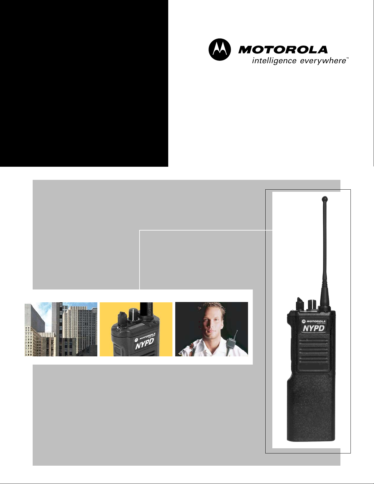
Special Note on NYPD Warranty Agreement
The three-year warranty on the NYPD SSE 5000 portable radio units represents the combination of the
standard one-year product warranty (detailed in this section) and the two-year Motorola Express Service Plus
(ESP) option. ESP is an extended service coverage plan, which provides for the repair of this product for an
additional period of two years beyond the expiration date of the standard warranty. For more information about
ESP, contact the Motorola Radio Support Center at 2200 Galvin Drive, Elgin IL 60123, (800) 422-4210 (U.S.
and Canada) / (847) 538-8023 (international).
Limited Warranty
MOTOROLA COMMUNICATION PRODUCTS
I. What This Warranty Covers And For How Long
MOTOROLA INC. (“MOTOROLA”) warrants the MOTOROLA manufactured Communication
Products listed below (“Product”) against defects in material and workmanship under normal use and
service for a period of time from the date of purchase as scheduled below:
SSE 5000 Portable Units Three (3) Years
Product Accessories One (1) Year
Motorola, at its option, will at no charge either repair the Product (with new or reconditioned parts),
replace it (with a new or reconditioned Product), or refund the purchase price of the Product during
the warranty period provided it is returned in accordance with the terms of this warranty. Replaced
parts or boards are warranted for the balance of the original applicable warranty period. All replaced
parts of Product shall become the property of MOTOROLA.
This express limited warranty is extended by MOTOROLA to the original end user purchaser only
and is not assignable or transferable to any other party. This is the complete warranty for the Product
manufactured by MOTOROLA. MOTOROLA assumes no obligations or liability for additions or
modifications to this warranty unless made in writing and signed by an officer of MOTOROLA.
Unless made in a separate agreement between MOTOROLA and the original end user purchaser,
MOTOROLA does not warrant the installation, maintenance or service of the Product.
MOTOROLA cannot be responsible in any way for any ancillary equipment not furnished by
MOTOROLA which is attached to or used in connection with the Product, or for operation of the
Product with any ancillary equipment, and all such equipment is expressly excluded from this
warranty. Because each system which may use the Product is unique, MOTOROLA disclaims
liability for range, coverage, or operation of the system as a whole under this warranty.
Page 14

xii Commercial Warranty
II. General Provisions
This warranty sets forth the full extent of MOTOROLA’S responsibilities regarding the Product.
Repair, replacement or refund of the purchase price, at MOTOROLA’s option, is the exclusive
remedy. THIS WARRANTY IS GIVEN IN LIEU OF ALL OTHER EXPRESS WARRANTIES. IMPLIED
WARRANTIES, INCLUDING WITHOUT LIMITATION, IMPLIED WARRANTIES OF
MERCHANTABILITY AND FITNESS FOR A PARTICULAR PURPOSE, ARE LIMITED TO THE
DURATION OF THIS LIMITED WARRANTY. IN NO EVENT SHALL MOTOROLA BE LIABLE FOR
DAMAGES IN EXCESS OF THE PURCHASE PRICE OF THE PRODUCT, FOR ANY LOSS OF
USE, LOSS OF TIME, INCONVENIENCE, COMMERCIAL LOSS, LOST PROFITS OR SAVINGS
OR OTHER INCIDENTAL, SPECIAL OR CONSEQUENTIAL DAMAGES ARISING OUT OF THE
USE OR INABILITY TO USE SUCH PRODUCT, TO THE FULL EXTENT SUCH MAY BE
DISCLAIMED BY LAW.
III. State Law Rights
SOME STATES DO NOT ALLOW THE EXCLUSION OR LIMITATION OF INCIDENTAL OR
CONSEQUENTIAL DAMAGES OR LIMITATION ON HOW LONG AN IMPLIED WARRANTY
LASTS, SO THE ABOVE LIMITATION OR EXCLUSIONS MAY NOT APPLY.
This warranty gives specific legal rights, and there may be other rights which may vary from state to
state.
IV. How To Get Warranty Service
You must provide proof of purchase (bearing the date of purchase and Product item serial number)
in order to receive warranty service and, also, deliver or send the Product item, transportation and
insurance prepaid, to an authorized warranty service location. Warranty service will be provided by
Motorola through one of its authorized warranty service locations. If you first contact the company
which sold you the Product, it can facilitate your obtaining warranty service. You can also call
Motorola at 1-888-567-7347 US/Canada.
V. What This Warranty Does Not Cover
A. Defects or damage resulting from use of the Product in other than its normal and customary
manner.
B. Defects or damage from misuse, accident, water, or neglect.
C. Defects or damage from improper testing, operation, maintenance, installation, alteration,
modification, or adjustment.
D. Breakage or damage to antennas unless caused directly by defects in material workmanship.
E. A Product subjected to unauthorized Product modifications, disassemblies or repairs
(including, without limitation, the addition to the Product of non-Motorola supplied equipment)
which adversely affect performance of the Product or interfere with Motorola's normal
warranty inspection and testing of the Product to verify any warranty claim.
F. Product which has had the serial number removed or made illegible.
G. Rechargeable batteries if:
- any of the seals on the battery enclosure of cells are broken or show evidence of
tampering.
- the damage or defect is caused by charging or using the battery in equipment or service
other than the Product for which it is specified.
H. Freight costs to the repair depot.
November 11, 2004 6881094C12-A
Page 15

Commercial Warranty xiii
I. A Product which, due to illegal or unauthorized alteration of the software/firmware in the
Product, does not function in accordance with MOTOROLA’s published specifications or the
FCC type acceptance labeling in effect for the Product at the time the Product was initially
distributed from MOTOROLA.
J. Scratches or other cosmetic damage to Product surfaces that does not affect the operation of
the Product.
K. Normal and customary wear and tear.
VI. Patent And Software Provisions
MOTOROLA will defend, at its own expense, any suit brought against the end user purchaser to the
extent that it is based on a claim that the Product or parts infringe a United States patent, and
MOTOROLA will pay those costs and damages finally awarded against the end user purchaser in
any such suit which are attributable to any such claim, but such defense and payments are
conditioned on the following:
A. that MOTOROLA will be notified promptly in writing by such purchaser of any notice of such
claim;
B. that MOTOROLA will have sole control of the defense of such suit and all negotiations for its
settlement or compromise; and
C. should the Product or parts become, or in MOTOROLA’s opinion be likely to become, the
subject of a claim of infringement of a United States patent, that such purchaser will permit
MOTOROLA, at its option and expense, either to procure for such purchaser the right to
continue using the Product or parts or to replace or modify the same so that it becomes
noninfringing or to grant such purchaser a credit for the Product or parts as depreciated and
accept its return. The depreciation will be an equal amount per year over the lifetime of the
Product or parts as established by MOTOROLA.
MOTOROLA will have no liability with respect to any claim of patent infringement which is based
upon the combination of the Product or parts furnished hereunder with software, apparatus or
devices not furnished by MOTOROLA, nor will MOTOROLA have any liability for the use of ancillary
equipment or software not furnished by MOTOROLA which is attached to or used in connection with
the Product. The foregoing states the entire liability of MOTOROLA with respect to infringement of
patents by the Product or any parts thereof.
Laws in the United States and other countries preserve for MOTOROLA certain exclusive rights for
copyrighted MOTOROLA software such as the exclusive rights to reproduce in copies and distribute
copies of such Motorola software. MOTOROLA software may be used in only the Product in which
the software was originally embodied and such software in such Product may not be replaced,
copied, distributed, modified in any way, or used to produce any derivative thereof. No other use
including, without limitation, alteration, modification, reproduction, distribution, or reverse
engineering of such MOTOROLA software or exercise of rights in such MOTOROLA software is
permitted. No license is granted by implication, estoppel or otherwise under MOTOROLA patent
rights or copyrights.
VII. Governing Law
This Warranty is governed by the laws of the State of Illinois, USA.
6881094C12-A November 11, 2004
Page 16

xiv Commercial Warranty
Notes
November 11, 2004 6881094C12-A
Page 17
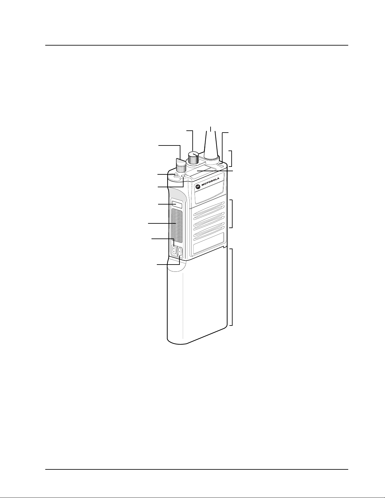
Chapter 1 Radio Description
1.1 Physical Features of the Radio
Figure 1-1 shows the physical features of the SSE 5000 portable radio.
On/Off/
Volume
Knob
Channel
Bank Select
Switch
Display
Button
Monitor
Button
PTT
Channel
Bank
Button
Secure
Button
Channel
Select
Knob
7
5
3
Antenna
5
1
1
P
Y
N
0
5
E
S
S
D
Transm it/
Receive
Indicator
(LED)
Control
Top
Display (1 line x 8 char,
bitmapped LCD)
0
0
Speaker/
Mic
Battery
The SSE 5000 portable radio operates in the UHF Range 2 (450–488 MHz) frequency band. It can
be programmed with up to 96 channels. Earlier versions of the radio, which could be programmed
with up to 48 channels, can be upgraded to 96-channel capability via FLASHport
1.2 FLASHport
The SSE 5000 radio utilizes Motorola’s FLASHport technology. FLASHport allows you to add
software that drives the radio’s capabilities, both at the time of purchase and afterwards. Previously,
changing a radio’s features and capabilities meant significant modifications, or buying a new radio.
Now the radio’s features and capabilities can be upgraded with FLASHport software, similar to how a
computer can be loaded with different software. For information on upgrading the radio’s features
using FLASHport, see the FLASHport User Guide (Motorola publication part number 6881094C35).
Figure 1-1. Physical Features of the SSE 5000 Radio
®
®
.
Page 18
1-2 Radio Description: Portable Radio Model Numbering System
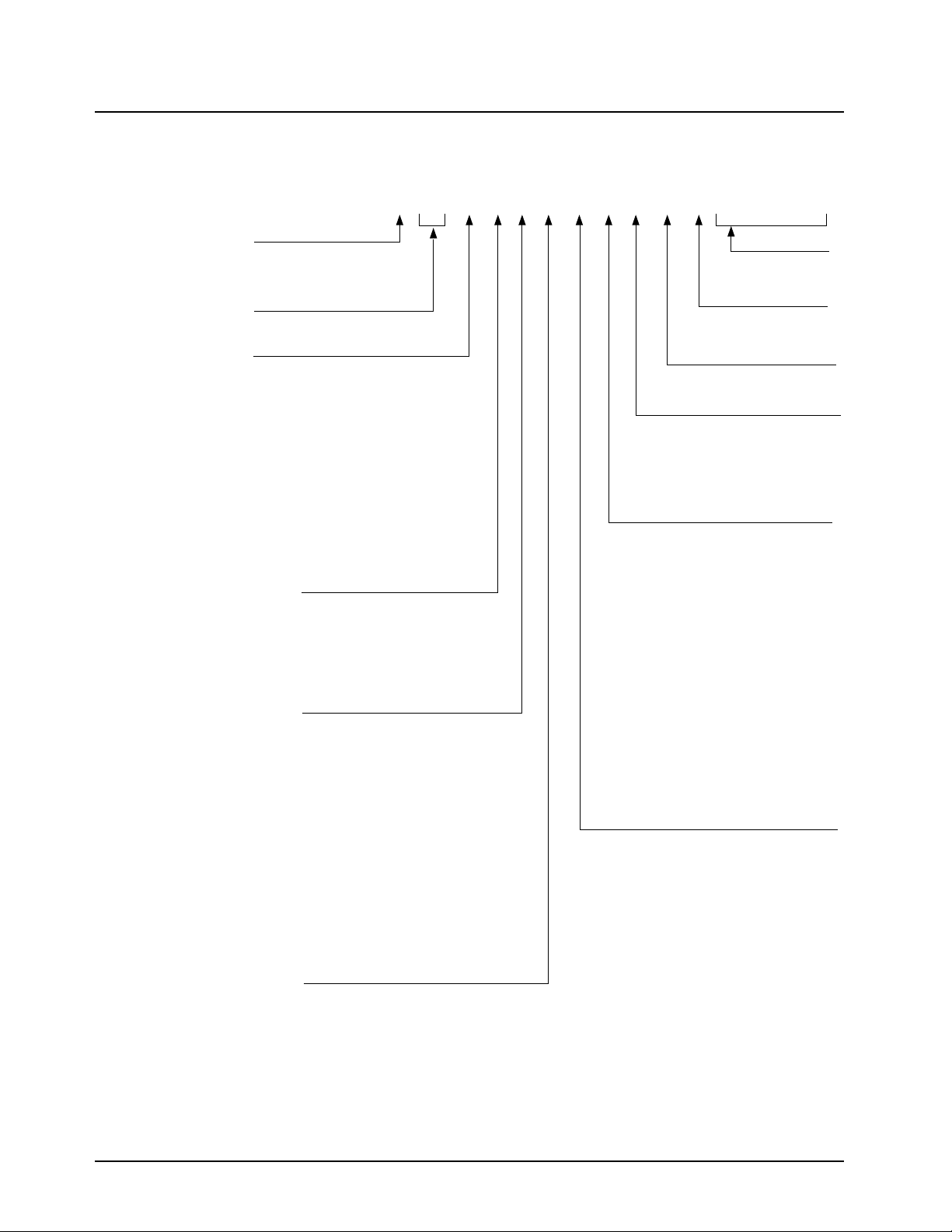
1.3 Portable Radio Model Numbering System
SSE5000ModelNumber:
Position:
Position1-TypeofUnit
H=Hand-HeldPortable
Positions2&3-ModelSeries
10=SSE5000
Position4-FrequencyBand
Lessthan29.7MHz
A
=
29.7to35.99MHz
B
=
36to41.99MHz
C
=
42to50MHz
D
=
66to80MHz
F
=
74to90MHz
G
=
ProductSpecific
H
=
136to162MHz
J
=
146to178MHz
K
=
174to210MHz
L
=
190to235MHz
M
=
Valuesgivenrepresentrangeonly;theyare
notabsolute.
Position5-PowerLevel
0to0.7Watts
A
=
0.7to0.9Watts
B
=
1.0to3.9Watts
C
=
4.0to5.0Watts
D
=
5.1to6.0Watts
E
=
6.1to10Watts
F
=
Position6-PhysicalPackages
RFModemOperation
A
=
ReceiverOnly
B
=
StandardControl;NoDisplay
C
=
StandardControl;WithDisplay
D
=
LimitedKeypad;NoDisplay
E
=
LimitedKeypad;WithDisplay
F
=
FullKeypad;NoDisplay
G
=
FullKeypad;WithDisplay
H
=
LimitedControls;NoDisplay
J
=
LimitedControls;BasicDisplay
K
=
LimitedControls;LimitedDisplay
L
=
RotaryControls;StandardDisplay
M
=
EnhancedControls;EnhancedDisplay
N
=
LowProfile;NoDisplay
P
=
LowProfile;BasicDisplay
Q
=
LowProfile;BasicDisplay,FullKeypad
R
=
Position7-ChannelSpacing
1=5kHz
2=6.25kHz
3=10kHz
4=12.5kHz
H10 S DD 9 P W 6 A N S P 0 1
123 4 56 7 8 910111213141516
P
=
Q
=
R
=
S
=
T
=
U
=
V
=
W
=
Y
=
Z
=
5=15kHz
6=20/25kHz
7=30kHz
9=Variable/Programmable
336to410MHz
403to437MHz
438to482MHz
470to520MHz
ProductSpecific
764to870MHz
825to870MHz
896to941MHz
1.0to1.6GHz
1.5to2.0GHz
Positions13-16
SPModelSuffix
Position12-
UniqueModelVariations
C=Cenelec
N=StandardPackage
Position11-Version
VersionLetter(Alpha)-MajorChange
Position10-FeatureLevel
1=Basic
2=LimitedPackage
3=LimitedPlus
4=Intermediate
5=StandardPackage
Position9-PrimarySystemType
A
=
Conventional
B
=
PrivacyPlus
C
=
ClearSMARTNET
D
=
AdvancedConventionalStat-Alert
E
=
EnhancedPrivacyPlus
F
=
Nauganet888Series
G
=
JapanSpecializedMobileRadio(JSMR)
H
=
Multi-ChannelAccess(MCA)
J
=
CoveragePLUS
K
=
MPT1327*-Public
L
=
MPT1327*-Private
M
=
Radiocom
N
=
ToneSignalling
P
=
BinarySignalling
Q
=
Phonenet
W
=
Programmable
X
=
SecureConventional
Y
=
SecureSMARTNET
6=StandardPlus
7=ExpandedPackage
8=ExpandedPlus
9=FullFeature/
Programmable
*MPT=MinistryofPostsandTelecommunications
Position8-PrimaryOperation
A
=
Conventional/Simplex
B
=
Conventional/Duplex
C
=
TrunkedTwinType
D
=
DualModeTrunked
E
=
DualModeTrunked/Duplex
F
=
TrunkedTypeI
G
=
TrunkedTypeII
H
=
FDMA*DigitalDualMode
J
=
TDMA**DigitalDualMode
K
=
SingleSideband
L
=
GlobalPositioningSatelliteCapable
M
=
AmplitudeCompandedSideband(ACSB)
P
=
Programmable
*FDMA=FrequencyDivisionMultipleAccess
**TDMA=TimeDivisionMultipleAccess
MAEPF-27326-A
November 11, 2004 6881094C12-A
Page 19
Radio Description: SSE 5000 UHF Range 2 (450–488 MHz) Model Chart 1-3
1.4 SSE 5000 UHF Range 2 (450–488 MHz) Model Chart
MODEL NUMBER DESCRIPTION
H10SDD9PW6AN UHF Range 2 (450–488 MHz), 2–5 Watts, SSE 5000
ITEM NUMBER DESCRIPTION
X — Antenna, UHF (Refer to Section A.1: “Antennas” on page A-1)
X — Battery (Refer to Section A.2: “Batteries” on page A-1)
X NUE7337_ Board, Transceiver, UHF Range 2 (450–488 MHz)
X NCN6186_ Board, VOCON *
X — Cable, Programming (Refer to Section A.8: “Programming Cables” on page A-2)
X — Case, Carrying (Refer to Section A.3: “Carrying Accessories” on page A-1)
X — Charger (Refer to Section A.4: “Chargers and Charger Accessories” on page A-1)
X NTN7061_ Cover, Accessory Connector
X NNTN4709_ Kit, Belt Clip
X NNTN4825_ Kit, Chassis, Back
X NNTN4826_ Kit, Chassis, Front
X 8485687E01 Kit, Control Flex
X NNTN4468_ Kit, Hardware
X NNTN4467_ Kit, Housing
X 8485791E01 Kit, Speaker Mic Flex
X — Mic Accessories (Refer to Section A.7: “Microphones and Microphone Accessories” on page A-2)
X NNTN4006_ Module, Encryption, DES, DES-XL, DES-PFB
X — Surveillance Accessories (Refer to Section A.9: “Surveillance Accessories” on page A-2)
X
Notes:
X = Item Included
* = When ordering a VOCON board, you will be asked to provide the radio's model number, FLASHcode, host
code, and DSP code. You can find this information as follows:
• For the radio model number and FLASHcode, place the radio in test mode (see Section 4.2: “Radio Test
Mode” on page 4-2) and view the scrolling displays.
• For the host code and DSP code, read the radio using the programming cable (RKN4121_ or RKN4122_)
and view the information in the CPS.
6881094C12-A November 11, 2004
Page 20

1-4 Radio Description: Specifications for UHF Range 2 (450–488 MHz) Radios
1.5 Specifications for UHF Range 2 (450–488 MHz) Radios
All specifications are per Telecommunications Industry Association TIA/EIA-603 unless otherwise
noted.
GENERAL RECEIVER TRANSMITTER
FCC Designation: AZ489FT4861
Temperature Range:
Operating: –30°C to +60°C
Storage: –40°C to +85°C
Power Supply: Nickel-Cadmium Battery (NiCd)
Battery Voltage:
Nominal: 7.5 Vdc
Range: 6 to 9 Vdc
Transmit Current Drain (typical)*:
5W RF Power: 1800 mA
2W RF Power: 1100 mA
Receive Current Drain at Rated Audio
(typical)*: 240 mA
Standby Current Drain (typical)*: 80 mA
Recommended Battery:
NiCd: NTN4595
or NiCd Smart: HNN9033
Optional FM (Factory Mutual) Battery:
NiCd FM: NTN4596*
or NiCd FM (HazMat): NTN4992*
or NiCd Smart FM: HNN9034*
* FM Intrinsically Safe.
Dimensions (H x W x D):
Without Battery (Radio Only):
H W
(no antenna) (at cntl top) (at cntl top)
4.7 in. 2.92 in. 1.37 in.
119.5 mm 74.2 mm 34.9 mm
(no antenna) (at bottom) (at PTT)
4.7 in. 2.66 in. 1.27 in.
119.5 mm 67.6 mm 32.2 mm
With Battery:
H W
(no antenna) (at cntl top) (at cntl top)
8.5 in. 2.92 in. 1.37 in.
215.9 mm 74.2 mm 34.9 mm
(no antenna) (at bottom) (at PTT)
8.5 in. 2.66 in. 1.27 in.
215.9 mm 67.6 mm 32.2 mm
D
D
Frequency Range: 450–488 MHz
Bandwidth: 38 MHz
Reference Sensitivity (12 dB SINAD) (typical):
0.25 µV
Intermodulation Rejection (typical): 75 dB
Adjacent Channel Rejection (typical):
25/30 kHz 78 dB
12.5 kHz 68 dB
Spurious Response Rejection (typical): 80 dB
Rated Audio Frequency Output Power:
500 mW
Hum and Noise Ratio (typical):
25 kHz 50 dB
12.5 kHz 43 dB
Audio Distortion (typical): 1.0%
Channel Spacing: 12.5/25 kHz
Frequency Range: 450–488 MHz
Conducted Carrier Output Power Rating:
450–488 MHz: 2–5 Watts
Carrier Frequency Stability (typical)
(–30 to +60°C; 25°C ref.): ±0.0002%
Conducted Spurious Emissions (typical):
70 dBc
FM Hum and Noise Ratio (typical)
(Companion Receiver): 25 kHz 50 dB
12.5 kHz 40 dB
Audio Distortion (typical): 1.5%
Modulation Limiting: 25 kHz ±5.0 kHz
12.5 kHz ±2.5 kHz
Adjacent Channel Power Ratio (ACPR)
(typical): 25 kHz 77 dBc
12.5 kHz 62 dBc
Emissions Designators:
20K0F1E, 16K0F3E, 11K0F3E, 8K10F1D, and
8K10F1E
Weight: (w/ Antenna):
Less Battery: 11.2 oz (316.9 gm)
With NiCd Smart: 15.9 oz (449.4 gm)
With NiCd: 13.7 oz (387.8 gm)
* Test box will add 25 mA.
Specifications subject to change without notice.
November 11, 2004 6881094C12-A
Page 21
Radio Description: Notations Used in This Manual 1-5
C
n
W
G
1.6 Notations Used in This Manual
Throughout the text in this publication, you will notice the use of note, caution, warning, and danger
notations. These notations are used to emphasize that safety hazards exist, and due care must be
taken and observed.
NOTE: An operational procedure, practice, or condition that is essential to emphasize.
!
a u t i o
!
!
A R N I N
!
D A N G E R
CAUTION indicates a potentially hazardous situation which, if
not avoided, might
WARNING indicates a potentially hazardous situation
which, if not avoided, could
DANGER indicates an imminently hazardous
situation which, if not avoided, will
injury.
result in equipment damage.
result in death or injury.
result in death or
6881094C12-A November 11, 2004
Page 22

1-6 Radio Description: Notations Used in This Manual
Notes
November 11, 2004 6881094C12-A
Page 23
Chapter 2 Theory of Operation
This chapter provides a detailed circuit description of the SSE 5000 transceiver and VOCON boards.
When reading the theory of operation, refer to the appropriate schematic and component location
diagrams located in the back of this manual. This detailed theory of operation can help isolate the
problem to a particular component.
The SSE 5000 radio is a dual-mode (digital/analog), microcontroller-based transceiver incorporating
a digital signal processor (DSP). The microcontroller handles the general radio control, monitors
status, and processes commands input from the keypad or other user controls. The DSP processes
the typical analog signals, and generates the standard signaling digitally to provide compatibility with
existing analog systems. In addition, the DSP provides digital modulation techniques, utilizing voice
encoding techniques with error correction schemes. This provides the user with enhanced range and
audio quality, all in a reduced bandwidth channel requirement. It allows embedded signaling, which
can mix system information and data with digital voice to support a multitude of system features.
The SSE 5000 radio operates within the UHF range (450 to 488 MHz).
2.1 Major Assemblies
The SSE 5000 radio includes the following major assemblies (see Figure 2-1):
• VOCON Board — contains a dual-core processor which includes both the microcontroller unit
(MCU) and a digital signal processor (DSP) core, the processor’s memory devices, an audio
and power supply support integrated circuit (IC), a digital-support IC, and the audio power
amplifier.
• Transceiver (XCVR) Board — contains all transmit, receive, and frequency generation
circuitry, including the digital receiver back-end IC and the reference oscillator.
• Controls/Universal Flex — contains on/off/volume switch, channel select switch, push-to-talk
(PTT) switch, monitor button, several function-selectable switches, universal connector,
speaker, and microphone.
• Display — 112 pixels x 32 pixels bit-mapped, liquid-crystal display (LCD).
Note:
Indicates12
wires
External
Accessory
Connector
7.5V
Battery
J101
J102
J1
Standard
Antenna
Remote
Antenna
3
MAEPF-27277-B
4
M102
20
J707
VOCON
20
14
Board
J301
J102
26
P201 P1
40
J701
Transceiver
Board
Encryption
Module
(Optional)
12
3
InternalSpeaker
& MicFlex
Control
Top
Display
Universal
Flex
12
Figure 2-1. SSE 5000 Overall Block Diagram
Page 24
2-2 Theory of Operation: Mode of Operation
2.2 Mode of Operation
This section provides an overview of the radio’s receive and transmit operation in the analog mode.
2.2.1 Receiving
When the radio is receiving (see Figure 2-2), the signal travels from the antenna connector to the
transceiver board, passing through the antenna switch and the receiver front-end. The signal is then
filtered, amplified, and mixed with the first local-oscillator signal, generated by the voltage-controlled
oscillator (VCO).
RXFrontEnd
LNA
CKO
Preselector
Filter
ADC
1stLO
1st
Mixer
3
MAEPF-27278-B
RX_SSI_DATA
toVOCONBoard
Remote
Port
Harmonic
Filter
RFInput
Harmonic
XTAL
Filter
Filter
Antenna
Switch
LO
Preselector
Filter
ABACUSIII-RXBackEnd
Figure 2-2. Receiver Block Diagram
The resulting intermediate frequency (IF) signal is fed to the IF circuitry, where it is again filtered and
passed to the Abacus III digital back-end IC. In the digital back-end IC, the IF signal is mixed with the
second local oscillator to create the second IF at 2.25 MHz. In the back-end IC, a bandpass, sigmadelta, analog-to-digital converter then decodes the second IF signal, and outputs, on the radio’s
serial synchronous interface (SSI) bus, digital audio to the VOCON board.
On the VOCON board, the dual-core processor’s digital-signal processor (DSP) digitally filters the
PCM audio. The DSP decodes the information in the signal and identifies the appropriate destination
for it.
• For a voice signal, the DSP will route the digital voice data to the CODEC inside the audio and
power supply support IC, for conversion to an analog signal. The CODEC will then present the
signal to the receive audio pre-amplifier, then to the audio power amplifier, which drives the
speaker.
• For signaling information, the DSP will decode the message and pass it internally to the
microcontrol unit of the dual-core processor.
November 11, 2004 6881094C12-A
Page 25
Theory of Operation: Mode of Operation 2-3
2.2.2 Transmitting
When the radio is transmitting, microphone audio is passed through gain stages to the CODEC,
where the signal is digitized (see Figure 2-3). The CODEC passes digital data to the DSP, where preemphasis and low-pass (splatter) filtering are done. The DSP passes this signal to a digital/analog
converter (DAC), where it is reconverted into an analog signal and scaled for application to the
voltage-controlled oscillator as a modulation signal.
TX_SSIfrom
VOCONBoard
RX_SSIto
VOCONBoard
PCIC
U104
Preselector
Filter
Power
Module
Q107
D101
RXLNA
Directional
Coupler
U101
Preselector
Filter
Dual
Antenna
Switch
Harmonic
MAEPF-27530-A
Filter
To
Remote
Port
To
Antenna
Reference
Oscillator
Y200
FracN
3
DAC
U203
FL200
SerialEE
3
LPF
PROM
U4
Sample
Clk
MOD
IN
ABACUSIIIU500
Loop
Filter
Note:
ThisUHFrangehas2VCOs
(1TX,1RX)
2ND
LO
VCO1
VCO2
Crystal
VCOBIC
Filter
TX
Buffer
Mixer
Amplifier
U102
TXDriver
Figure 2-3. Transceiver (UHF Range) Block Diagram (Power and Control Omitted)
Transmitted signaling information is applied to the DSP from the microcontrol unit, where it is coded,
and passed to the DAC, which handles it the same as a voice signal. The DAC output connects to
the synthesizer modulation input. A modulated carrier is provided to the transmitter power amplifier,
which transmits the signal under dynamic power control.
6881094C12-A November 11, 2004
Page 26
2-4 Theory of Operation: Power Distribution
2.3 Power Distribution
This section provides a detailed circuit description of the power distribution of the SSE 5000 radio.
In the SSE 5000 radio, power (B+) is distributed to two boards: the transceiver (RF) board and the
VOCON board (see Figure 2-4). In the case of a secure radio, B+ is also supplied to the encryption
module.
FET
1.55V
VOCONBoard
VCC5
SW_B+
3.8V(VSW1)
1.875Volts
(VSW2)
(VREF)
5Volts
GCAPII
2.893
2.893
Volts Volts
(V2)
MAEPF-27419-A
Battery
7.5Volts
(Nominal)
RFBoard
J1
BATT FB+
RAWB+
Fuse
FET
XB+
(controlsignal)
V5A
5Volts
V3A V3D
3Volts
AnalogCircuits
3Volts
DigitalCircuits
P1
UNSW_B+
P201
1.55Volts
(VSW_1.55)
Figure 2-4. DC Power Distribution—UHF Radios
Power for the radio is provided through a battery supplying a nominal 7.5 Vdc directly to the
transceiver. The following battery types and capacities are available:
Table 2-1. Conventional Batteries
Part Number Description
NTN4595 Premium NiCd (1800 mAh, 7.5 V)
NTN4596 Premium NiCd FM (1800 mAh, 7.5 V)
NTN4992 Premium NiCd FM (1800 mAh, 7.5 V) (HazMat)
Table 2-2. Smart Batteries
Part Number Description
HNN9033 impres™ NiCd (2000 mAh)
HNN9034 impres™ NiCd FM (2000 mAh)
B+ from the battery is electrically switched to most of the radio, rather than routed through the On/
Off/Volume knob. The electrical switching of B+ supports a keep-alive mode. Under software control,
November 11, 2004 6881094C12-A
Page 27
Theory of Operation: Power Distribution 2-5
even when the On/Off/Volume knob has been turned to the off position, power remains on until the
microcontroller unit (MCU) completes its power-down, at which time the radio is physically powered
down.
2.3.1 DC Power Routing—Transceiver Board
Connector J1, the B+ assembly, connects the battery to the transceiver board. Two capacitors
provide protection against momentary breaks at the B+ connector due to contact bounce when the
radio is dropped.
An RF bead forms a power-line filter for signal RAWB+, which supplies battery voltage to the
transmitter PA.
A transistor, controlled by signal SWB+ from the VOCON board, turns on XB+, which supplies the
5-V linear regulator, TX_ALC block and SW_FL.
Fuse F901 and a filter supply fused B-plus to the VOCON board. In turn, the VOCON board supplies
VSW1, regulated 3.8 Vdc, from the Global Control Audio and Power (GCAP) switching regulator to
the XCVR. A switch, controlled by SWB+, turns on V38 to the XCVR 3-V linear regulators. The
XCVR regulated power supplies are summarized in Table 2-3.
Table 2-3. Transceiver Voltage Regulators
IC
Name
LP2989 V5A Regulated 5.0 Vdc
LP3985 V3D Regulated 3.0 Vdc digital
LP3985 V3A Regulated 3.0 Vdc analog for the RX FE
Output
Signal Name
Description
2.3.2 DC Power Routing—VOCON Board
Raw B+, or unswitched B+, (UNSW_B+) is routed to connector J1 on the transceiver board, and then
on to P201 on the VOCON board. Here the UNSW B+ is forwarded to the radio’s control top
On/Off/Volume knob through connector J707 and a flex circuit, as well as to regulator U505 (VCC5).
The On/Off/Volume knob controls B+SENSE to a BJT switch, which in turn controls a power
MOSFET. The MOSFET is a solid-state power switch that provides SW B+ to the VOCON board, the
audio PA, the GCAP II IC (via GCAP_B+), and back to the transceiver board.
In the case of a secure radio model, SW B+ and UNSW B+ are also supplied to the encryption
module through connector J701.
The BJT switch is also under the control of the MCU via Vref from the GCAP II IC (U501). This allows
the MCU to follow an orderly power-down sequence when it senses that B+SENSE is off. This sense
is provided through MECH_SW_BAR (inverted B+SENSE).
The digital circuits in the VOCON board are powered from regulators located in the GCAP II IC
(U501), an external 5 Vdc regulator (VCC5, U505), and an external 1.55 Vdc regulator (VSW_1.55).
The GCAP II IC provides three supplies: VSW1, VSW2, and V2. These regulators are software
programmable.
6881094C12-A November 11, 2004
Page 28

2-6 Theory of Operation: Power Distribution
Table 2-4 lists the supply voltages and the circuits that use these voltages.
Table 2-4. VOCON Board DC Power Distribution
Supply
Name
UNSW_B+ 9 to 6 Vdc
SW_B+ 9 to 6 Vdc
VCC5 5Vdc Linear regula-
VSW1 3.8 Vdc Switching
VSW2 1.8 Vdc Switching
Output
Voltage
7.5 Vdc
nominal
7.5 Vdc
nominal
Supply Type
Battery N/A VCC5 input
Battery N/A VSW1 input (GCAP)
tor
regulator
software programmable
regulator
software programmable
Unprogrammed
Output Voltage
N/A Smart battery circuitry
3.2 Vdc 3-V regulators (RF)
2.2 Vdc Dual-core processor’s external
Circuits Supplied
Mechanical switch
Power switch (FET)
Secure module
Audio power amplifier
Side connector
SW_B+ to transceiver board
GCAP IC
Secure module
USB circuitry
Int. / ext. microphone bias
Audio preamplifier
Digital-support IC
Display LEDs
VSW2 input
V2 input
1.55 V regulator bias
memory interface
FLASH IC
SRAM
1.55 V regulator bias
VSW_1.55 1.55 Vdc Linear regula-
tor
V2 2.893 Vdc Switching
regulator
software programmable
November 11, 2004 6881094C12-A
N/A Dual-core processor core
2.775 Vdc Dual-core processor’s I/O ring
Digital-support IC
EEPOT
Display
16.8 MHz buffer
Page 29
Theory of Operation: Transceiver Board 2-7
2.4 Transceiver Board
The transceiver (XCVR) board performs the transmitter and receiver functions necessary to translate
between voice and data from the VOCON board and the modulated radio-frequency (RF) carrier at
the antenna. The transceiver board contains all the radio’s RF circuits for the following major
components:
• Receiver
• Transmitter
• Frequency Generation Unit (FGU)
2.4.1 Interconnections
This section describes the various interconnections for the transceiver board.
2.4.1.1 Battery Connector J3
Battery connector J3 consists of three gold-plated contacts on the printed circuit board that mate with
a B-plus connector assembly. Signal descriptions are in Table 2-5.
Table 2-5. Battery Connector J3
Pin No. Signal Description
1 BATT Battery positive terminal, nominally 7.5 Vdc
2 BSTAT Battery status, from battery to VOCON
3 BAT_RTN Battery negative terminal, tied to PCB ground
2.4.1.2 VOCON Connector P1
VOCON connector P1 (located on the XCVR board) consists of 26 gold-plated pads for the 26-pin
compression connector, and one plated tool hole (pin 27) used for connector alignment. This is a
digital interface carrying DC power, control, and data between the XCVR and VOCON boards. P1
connects through the compression connector to P201 on the VOCON board.
Table 2-6 lists the connector pins, their signals, and functions. SPI refers to the serial peripheral
interface, which is the control bus from the microprocessor. SSI is the serial synchronous interface
bus for data to and from the DSP. There is a RX SSI bus for demodulated data from the receiver and
a TX SSI bus for modulation data to the transmitter.
Pin No. VOCON Signal
1 UNSW_B+ FUB+ O dc Fused B+ to VOCON
2 UNSW_B+ FUB+ O dc Fused B+ to VOCON
Table 2-6. VOCON Connector P1
XCVR
Signal
XCVR
I/O
Type Description
3 LOCK_DET* LOCK O status FGU lock detect
4 TX_SSI_DATA TXTD O ssi TX SSI data
5 SSI_CLK RXCK O ssi RX SSI clock
6881094C12-A November 11, 2004
Page 30
2-8 Theory of Operation: Transceiver Board
Table 2-6. VOCON Connector P1 (Continued)
Pin No. VOCON Signal
6 SSI_FSYNC RXFS O ssi RX SSI frame sync
7 16.8MHz F168 O RF 16.8 MHz reference clock
8 SW_B+ SWB+ I dc Switch control
9 TX_SSI_FSYNC TXFS I ssi TX SSI frame sync
10 TX_SSI_CLK TXCK I ssi TX SSI clock
11 AD4_RF_BD_ID RF_BD_ID O dc RF board ID
12 RX_SSI_DATA RXDO O ssi RX SSI data
13 ABACUS3_CS ABCS I ssi SPI Abacus chip select
14 GND GND
15 VSW1 VSW1 I dc Regulated 3.8 V
16 SPI_CLK_A SPCK I spi SPI clock
17 SPI_MISO_A MISO O spi SPI data out
18 EEPROM_SEL* EECS I spi SPI EEPROM chip select
19 TX_INHIBIT TXINH I control TX inhibit control for secure
XCVR
Signal
XCVR
I/O
Typ e Description
20 GND GND
21 BAT_STATUS BSTAT O dc Battery status
22 GND GND
23 SPI_MOSI_A MOSI I/O spi SPI data I/O
24 UNI_CS USEL I spi SPI universal chip select
25 RF_RX_ATNR RX_ATNR I dc RF RX attenuator
26 POR* RSTL I/O control asynchronous reset, active low
2.4.1.3 Antenna Ports
Antenna port J101 is a hot launch connector that interfaces to the antenna connector that is part of
the control top. This interface provides the launch mechanism for the antenna. Antenna port J102
provides RF to the accessory RF connector on the back of the SSE 5000 radio. This port provides
RF energy for tuning purposes, as well as RF for a public safety microphone.
2.4.1.4 Serial EEPROM
The serial, electrostatically erasable, programmable, read-only memory (EEPROM) has the
reference designator U4 on the SSE 5000 transceiver board. This IC holds all of the transceiver
tuning data. This allows transceivers to be tuned in the factory and installed in the field without
retuning.
November 11, 2004 6881094C12-A
Page 31

Theory of Operation: Transceiver Board 2-9
2.4.1.5 Power Conditioning Components
DC power-conditioning components include zener diodes, capacitors, ferrite beads, a power
inductor, and the fuse. Diodes VR1 and VR2 provide over-voltage protection. Ferrite beads
(designated E1, E4, E101) and capacitors suppress electromagnetic interference from the
transceiver. The power-line filter consisting of L1, C13, and C14 suppresses digital noise from the
VOCON board switching power supplies that could degrade the transmitter spectral purity.
Pass transistor Q1 switches the battery voltage to the transceiver when control signal SWB+ or SB+
from the VOCON board is asserted high. This increases the transceiver’s immunity to conducted
interference that might be present on SWB+ or SB+, such as from switching voltage regulators on
the VOCON board.
Ground clip G9 makes contact between the transceiver board ground and the radio chassis. The
chassis connection is a necessary electrical reference point to complete the antenna circuit path.
Shields SH201 through SH702 and the tool hole appear on the schematic to show their connection
to ground.
2.4.2 Receiver
The SSE 5000 transceiver has a dual-conversion superheterodyne receiver. Figure 2-2 illustrates
the major receiver components:
• Receiver front-end
• Receiver back-end
2.4.2.1 Receiver Front-End
NOTE: Refer to Figure 2-2 for the receiver block diagram, Table 2-7 for local oscillator (LO) and first
IF information, and Figure 12-2 for the receiver front-end schematic.
The receiver front-end tunes to the desired channel and down converts the RF signal to the first
intermediate frequency (IF). Channel selection is by way of a tunable local oscillator, RXLO, from the
FGU.
Table 2-7. Local Oscillator and First IF Frequencies
The receiver front-end consists of a preselector filter, an RF amplifier, a second preselector, mixer,
and an IF crystal filter. The SSE 5000 radio also contains a switchable attenuator between the
antenna switch and the first preselector filter. The RF amplifier is a discrete RF transistor with
associated circuitry. The mixer is a double-balanced, active mixer IC, coupled by transformers. The
receiver (RX) local oscillator (LO) is provided by the FGU.
2.4.2.1.1 Preselector Filters
UHF Range 2
(450–488 MHz)
LO Frequency Range 376.65–414.65 MHz
First IF Frequency 73.35 MHz
The receiver front-end uses two discrete bandpass filters to achieve its required out-of-band
rejection. The first preselector filter precedes the RF amplifier, while the second preselector filter
follows the RF amplifier.
6881094C12-A November 11, 2004
Page 32

2-10 Theory of Operation: Transceiver Board
2.4.2.1.2 LNA (Low-Noise Amplifier)
The SSE 5000 radio uses a discrete transistor for the low-noise amplifier (Q430). A feedback
network between the collector and base improves stability and gain balance across the frequency
band. Input and output LC networks match the LNA impedance to 50 ohms.
A diode limiter (D400) protects the amplifier damage by strong input signals.
2.4.2.1.3 Mixer
The mixer (U470) down-converts the received RF to the first intermediate frequency (IF). The IF is
73.35 MHz. Low-side LO injection is used. Transformers are used as baluns to convert signals from
single-ended to balanced at pins MI, MIX, LO, and LOX. An output transformer converts the
balanced signal at pins MO and MOX to a single-ended output.
2.4.2.1.4 IF Filter
The IF filter (FL400) is a leadless, surface-mount, 3-pole, quartz crystal filter. This narrow bandpass
filter gives the radio its adjacent-channel and alternate-channel rejection performance.
Input and output LC networks match the filter impedance to 50 ohms.
2.4.2.2 Receiver Back-End
NOTE: Refer to Figure 2-2 for the receiver block diagram and Figure 12-3 for the receiver back-end
schematic.
The receiver back-end, which consists of the Abacus III (AD9874 IF digitizing subsystem) IC and its
associated circuitry, processes the down-converted IF signal to produce digital data for final
processing by the VOCON DSP.
2.4.2.2.1 Abacus III IC U500
The AD9874 is a general-purpose, IF subsystem that digitizes a low-level 10–300 MHz IF input with
a bandwidth up to 270 kHz. The output of the Abacus III IC is SSI data to the VOCON.
The signal chain of the AD9874 consists of a low-noise amplifier, a mixer, a bandpass sigma-delta
A/D converter, and a decimation filter with programmable decimation factor. An automatic gain
control (AGC) circuit provides the AD9874 with 12 dB of continuous gain adjustment. The high
dynamic range and inherent anti-aliasing provided by the bandpass sigma-delta converter allow the
AD9874 to cope with blocking signals 80 dB stronger than the desired signal.
Auxiliary blocks include frequency synthesizers for the second LO and sampling clock LO, as well as
an SPI port. The second LO uses a discrete external loop filter and VCO. The clock oscillator has an
external loop filter and resonator.
November 11, 2004 6881094C12-A
Page 33

Theory of Operation: Transceiver Board 2-11
MXON
IF2P
MXOP
IF2N
GCP
GCN
IFIN
FREF
AD9874
-16dB
LNA
LO
Synth.
IOUTL
LOVCOand
LoopFilter
LOP
LON
M
Samp.Clock
Synthesizer
CLKP
IOUTC
CLKVCOand
LoopFilter
ADC
......=13-26MHz
CLKN
DAC AGC
Decimation
Filter
Voltage/
Current
Reference
VREFP
RREF
VREFN
Formatting/SSI
ControlLogic
SPI
PC
PD
DOUTA
DOUTB
FS
CLKOUT
PE
SYNCB
MAEPF-27412-O
Figure 2-5. Abacus III (AD9874) Functional Block Diagram
Input signal RXIF is 73.35 MHz IF from crystal filter FL400 in the receiver front-end. Components
L547 and C542 match the input impedance to 50 ohms. Formatted SSI data is output to the VOCON
board on ports FS, DOUTA, and CLKOUT.
2.4.2.2.2 Second Local Oscillator
The second LO is controlled by the Abacus LO synthesizer, which mixes with IFIN to produce a 2.25
MHz final IF. The external VCO consists of Q502 and its bias network and frequency-determining
elements. Signal FREF is the 16.8 MHz reference from the FGU. Darlington transistor Q501 with
C550 and R501 form an active power-line filter.
The second LO frequency is 71.1 MHz by default or 75.6 MHz in special cases as needed to avoid
radio self-quieters. The loop filter is composed of R551, C558, C559, R552, and C512.
2.4.2.2.3 Sampling Clock Oscillator
The Abacus sampling clock synthesizer operates at 18 MHz = 8 x 2.25 MHz. The VCO uses an
internal transistor and external resonator. The resonator is composed of L503, C535, C929, and
D501.
The loop filter is composed of R512, C536, R514, C570, and C571.
2.4.3 Transmitter
NOTE: Refer to Figure 2-6 for the transmitter block diagram and Figure 12-4 for the transmitter
schematic.
The transmitter takes modulated RF from the FGU and amplifies it to the radio’s rated output power
to produce the modulated transmitter carrier at the antenna.
The transmitter consists of an RF driver IC that receives its input signal from the voltage-controlled
oscillator (VCO) and a high-power output transistor. Transmitter power is controlled by a power-
6881094C12-A November 11, 2004
Page 34

2-12 Theory of Operation: Transceiver Board
control IC (PCIC) that senses the output of a directional coupler and adjusts PA control voltages to
maintain a constant power level. The signal passes through a dual antenna switch and harmonic
filters to the antenna or to the remote RF port.
amplifier
ModulatedRF
fromFGU
2.4.3.1 Power Distribution
To minimize voltage drop to the power amplifiers, net RAWB+ connects to power module Q107 and
the second stage of driver amplifier U102 through components having minimal series resistance—
ferrite beads and chokes only. During receive, no RF or DC bias is applied, and leakage current
through U102 and Q107 is less than 100 microamps.
At the rated transmitter power of 5 Watts, the radio consumes approximately 1800 mA, and at the
rated transmitter power of 2 Watts the radio consumes approximately 1100 mA.
Driver
INT
Power
amplifier
PCIC
Directional
V
V
V
V
V
RFIN
RX
coupler
Forwardpowerdetector
Vd=m*sqrt(P)+b
Figure 2-6. Transmitter Block Diagram
Dual
Antenna
switch
Harmonic
filters
To
Remote
RF
MAEPF-27408-O
Antenna
2.4.3.2 Driver Amplifier
The driver amplifier IC (U102) contains two LDMOS FET amplifier stages and two internal resistor
bias networks. Pin 16 is the RF input. Modulated RF from the FGU, at a level of +3 dBm ±2 dB, is
coupled through a DC blocking capacitor to the gate of FET-1. An LC interstage matching network
connects the first stage output VD1 to the second stage input G2. The RF output from the drain of
FET-2 is pin 6 (RFOUT1). Gain control is provided by a voltage applied to pin 1 (VCNTRL). Typical
output power is about +27 dBm (500 mW) with VCNTRL at 5.0 V.
L109 and C113 are the interstage matching network. Components L105 and C110 match the output
impedance to 50 ohms; capacitor C107 is a DC block.
2.4.3.3 Power Amplifier Transistor Q107
The power amplifier transistor, Q107, is an LDMOS FET housed in a high-power, surface-mount, ring
package. To prevent thermal damage, it is essential that the heat sink of the power module be held in
place against the radio chassis. The input impedance-matching network uses discrete inductors and
capacitors. The low-pass output matching network uses both transmission lines and lumped LCs.
Drain bias is applied through E101 and L101. Gain is dynamically controlled by adjusting the gate
bias. The gate is insulated from the drain and source so that gate bias current is essentially zero.
The input impedance-matching network is L106, L107, C108, and C109. A transmission-line
structure and C137, C111, L110 and C112 form the output-matching network. Gate bias is applied
through R105 and L108.
November 11, 2004 6881094C12-A
Page 35

Theory of Operation: Transceiver Board 2-13
2.4.3.4 Directional Coupler
A directional coupler senses the transmitter forward power as a control signal in the transmitter’s
automatic level control (ALC) loop. Isolated ports are terminated with external resistors.
The directional coupler is U101, a low-loss, bidirectional coupler.
2.4.3.5 Antenna Switch
The SSE 5000 has two antenna switches: one standard antenna switch and a remote antenna
switch.
The standard antenna switch is a quarterwave switch that determines whether the radio is in receive
or transmit mode. The standard antenna switch consists of part numbers D701, D702, C706, C704,
C701, C707, L702, L703, and R701. When the standard antenna switch is in receive mode, the
diodes D701 and D702 are unbiased and radio signals are able to travel to the receive front-end.
When the standard antenna switch is in transmit mode, radio signals travel from the transmitter to
the selected port and radio signals from the transmitter to the receive front-end are redirected by the
large impedance presented by L702 and C704. The receive front-end is also protected from the
transmitter because of the combined effect of the radio wave redirection and the short produced by
C703 when the standard antenna switch is enabled.
The circuitry that enables the standard antenna switch consists of part numbers L703, C707, and
U104. When the radio is in transmit mode, pin 32 (also known as ANO) on U104 provides
approximately 6.7 volts to diode D702. This voltage is dropped approximately 1.4 volts, or two diode
drops, and applied to R701. R701 sets the current through the antenna switch (approximately 14
mA). L703 and C707 are used as a DC bias network designed to only transmit DC signals.
The remote antenna switch is also a quarterwave switch, but this switch determines which antenna
the radio uses for transmit or receive. The remote antenna switch consists of part numbers D602,
D601, C724, C725, C726, C727, C728, L701, L704, L711, R703, R704, R705, Q702, and Q703.
When the radio is receiving from the standard antenna, no diodes are forward biased. In order to
activate the remote antenna port, the VOCON must supply 2.9 volts (+/– 3%) to pin 19 of the 26-pin
connector. Pin 19 is also known as TX_INH. TX_INH going high causes the voltage on the collector
of Q703 to become the voltage on the emitter. The voltage on the emitter for this circuit is zero volts.
The collector is connected to the gate of Q702, which in turn forces the voltage on the drain of Q702
to become the voltage on the source of Q702. The voltage on the source of Q702 is switched B+, or
battery voltage. Switched B+ is dropped approximately 1.4 volts, or two diode drops, and applied to
R705. R705 sets the current through the remote port switch (approximately 12 mA).
L701 and C724 are used as a DC bias network designed to only transmit dc signals. When the radio
is receiving or transmitting through the remote port, radio signals travel through diode D602. The
signals are directed away from the standard antenna by the large impedance presented by L704 and
C727. Accidental radiation through the standard antenna is prevented, because of the combined
effect of the radio wave redirection and the short produced by C725 when the remote port is
enabled.
NOTE: Part numbers C728 and L711 are used to resonate the parasitic capacitance created by diode
D602. The parasitic capacitance was creating a degradation in the transmit response through
the standard antenna port. Essentially, C728 is a DC block to prevent reverse biasing D602,
and L711 resonates with the parasitic capacitance of D602 to create a large impedance.
2.4.3.6 Harmonic Filter
RF from the power amplifier is routed through the coupler (U101), passed through the antenna
switch, passed through the remote port switch, and applied to a harmonic filtering network. The SSE
5000 harmonic filters are five-pole elliptical low-pass filters.
6881094C12-A November 11, 2004
Page 36

2-14 Theory of Operation: Transceiver Board
The initial design utilizes a cutoff frequency of 750 MHz, even though the actual design cutoff
frequency is 488 MHz. The reasoning behind using a significantly higher cutoff frequency is due to
the lower frequency response of realized circuits. The design tables used for the filter synthesis can
be located in the Handbook of Filter Synthesis (Zverev, pp. 218–219), where θ = 47.0. This design
was chosen because the attenuation at the stop band was the closest to the desired ratio for the
SSE 5000 design.
The remote port harmonic filter consists of parts C709, C710, C711, C712, C713, L706, and L707.
The antenna port harmonic filter consists of parts C716, C717, C718, C719, C720, L709, and L710.
The filters are optimized for the impedance match seen for their respective ports and terminations.
NOTE: Capacitor C720 was changed to 2pF, because this value improved the radiated response of
the radio with the antenna removed. Also, Capacitors C710 and C711 were increased in order
to remove a spur located at the (2*LO)-IF frequency point (680.075 MHz), where LO is
450.0625 MHz – 73.35 MHz and IF is 73.35 MHz. Essentially, C710 and C711 decreased the
cutoff frequency of the remote port harmonic filter.
2.4.3.7 RF Detector D101
Schottky diode D101 is used as a forward-power detector. Forward-coupled RF from the power
amplifier is converted to a DC voltage. Detector output is a positive DC voltage, proportional to the
amplitude of the RF signal at the input, and is applied to the ALC input of the PCIC.
2.4.3.8 Power-Control IC (PCIC) U104
The PCIC, U104, contains all of the digital, and most of the analog, circuits needed to control the
transmitter power amplifier. Host control is through a 3-wire, smart SPI interface. Pin descriptions are
shown in Table 2-8.
Table 2-8. Power Control IC (U104) Pin Descriptions
Pin Name Description
1 RFIN Detector voltage input to ALC
2 T1 Test point
3 CI External capacitor for integrator time constant
4 INT Integrator output; control voltage to amplifiers
5 CJ External capacitor for PA rise and fall times
6, 7 VL, CL External capacitor for PA rise and fall times
8 GND1 Ground
9 F168 Reference clock input, 2.1 MHz
10, 13 QX, CQX External capacitor for voltage multiplier
11, 12 Q, CQ External capacitor for voltage multiplier
14 V10 Voltage multiplier output
15 VG Internal band-gap reference voltage
16 V45 Regulated 4.5 Vdc output
17 V5EXT Power supply input for internal voltage regulator
November 11, 2004 6881094C12-A
Page 37

Theory of Operation: Transceiver Board 2-15
Table 2-8. Power Control IC (U104) Pin Descriptions (Continued)
Pin Name Description
18 VAR2 Buffered D/A output
19 VLIM Test point for internal D/A No.2 voltage
20 VAR1 Buffered D/A output
21 RS Asynchronous reset input
22 NA Spare pin
23 RX RX/TX mode control-bit output
24 VAR3 Buffered D/A output
25 GND2 Ground
26 CLK SPI clock input
27 BPOS Power supply input
28 DATA SPI data input/output
29 CEX SPI chip select input
30 TEMP Temperature sensor input
31 RSET External resistor; used to set the temperature cutback rate
32 ANO Switched BPOS output
2.4.3.8.1 Power and Control
Since U104 is powered from switched B+, it makes its own regulated 4.5 Vdc to power the internal
logic. The supply input is V5EXT at pin 17, and the output is V45 at pin 16. ANO at pin 32 is the
control signal to the RX/TX antenna switch control circuit.
2.4.3.8.2 Automatic Level Control (ALC)
In TX mode, the PCIC disables the receiver, turns on the transmitter, and controls the TX power
level. The automatic level control (ALC) circuit operates as follows:
The power level is set by programming an internal DAC to a calibrated reference voltage. D/A
settings for the power set points were determined during radio tuning and stored in EEPROM. An
internal op-amp compares the D/A reference voltage to the detector voltage at pin 1(RFIN) (TP101)
and produces an error signal output. This signal is buffered by another op-amp, configured as a lowpass filter, or integrator, to produce the INT output at pin 4 (TP111).
This INT output supplies voltage to drive the gain control pins of amplifiers U102 and Q107.
Resistors R105 and R106 determine the voltage ratio between U102 pin 1 (VCNTRL) and the Q107
gate. Transient response during key-up and key-down is controlled by the power amplifier rise and
fall times. External capacitors at pins CI, CJ, and CL, along with internal programmable resistors,
determine the ALC time constants.
2.4.3.8.3 Temperature Cut Back
The PCIC contains a temperature cut-back circuit to protect the power amplifier (PA) from thermal
damage that might result from incorrect assembly of the radio. External sensor U103 is a linear
temperature-to-voltage transducer, placed near the hottest spot in the radio: power module Q107.
6881094C12-A November 11, 2004
Page 38

2-16 Theory of Operation: Transceiver Board
The output is a DC voltage at pin 2 (VOUT) proportional to the temperature at pin 3 (GND). VOUT is
750 mV at 25°C and increases by 10 mV/°C. The PCIC temperature cut-back threshold is
programmed to correspond to 85 or 90°C. Above this threshold, the ALC gradually cuts back the
transmitter until it is fully turned off at 125°C. The slope of cut-back versus temperature is set by
external resistor R111. Diode D104 clamps TEMP to a voltage not much less than VG (pin 15), about
1.3 V, to improve the transient response of the cut-back circuit.
2.4.4 Frequency Generation Unit (FGU)
The frequency-generation function is performed by several ICs, two voltage-controlled oscillators
(VCOs) (one transmit and one receive), and associated circuitry. The reference oscillator provides a
frequency standard to the fractional-N frequency synthesizer (FracN) IC, which controls the VCOs
and VCO buffer IC (VCOBIC). The VCOBIC amplifies the VCO signal to the correct level for the next
stage.
NOTE: Refer to Figure 12-5 and Figure 12-6 for the FGU schematics.
2.4.4.1 Reference Oscillator Y200
The radio’s frequency stability and accuracy derive from the Voltage-Controlled TemperatureCompensated Crystal Oscillator (VCTCXO), Y200. This 16.8 MHz oscillator is controlled by the
voltage from the WARP pin of the FracN IC, U202, that can be programmed through a serial
peripheral interface (SPI). The oscillator output at pin 3 is coupled through capacitor C234 to the
FracN synthesizer reference oscillator input and through C236 to the non-invertive input of the opamp, U201.
Op-amp U201 buffers the 16.8 MHz output to the VOCON board. Components L205 and C214 form
a low-pass filter to reduce harmonics of the 16.8 MHz.
The Digital-to-Analog Converter (DAC) IC, U203, and Switched Capacitors Filter (SCF) IC, FL200,
form the interface between radio's DSP and the analog modulation input of the FracN IC.
2.4.4.2 Fractional-N Frequency Synthesizer (FracN) IC U202
The FracN IC, U202, is a mixed-mode, Motorola-proprietary, CMOS, fractional-N frequency
synthesizer with built-in dual-port modulation. The SSE 5000 radio uses a low-voltage version of the
device, sometimes called LVFracN, for compatibility with the 3 V logic used throughout the radio.
The FracN IC incorporates frequency division and comparison circuitry to keep the VCO signals
stable. The FracN IC is controlled by the MCU through a serial bus. All of the synthesizer circuitry is
enclosed in rigid metal cans on the transceiver board to reduce interference effects.
Separate power supply inputs are used for the various functional blocks on the IC. Inductors L203
and L204 provide isolation between supply pins 20 (AVDD) and 36 (DVDD) connected to Vdd3. Host
control is through a three-wire, smart SPI interface (pins 7, 8, and 9) with a bi-directional data pin.
FracN functions include frequency synthesis, reference clock generation, modulation control, voltage
multiplication and filtering, and auxiliary logic outputs.
2.4.4.2.1 Synthesizer
Frequency synthesis functions include a dual-modulus prescaler, a phase detector, a programmable
loop divider and its control logic, a charge pump, and a lock detector output. Fractional-N synthesizer
IC principles of operation are covered in detail in the manufacturers’ literature. No similar discussion
will be attempted here.
2.4.4.2.2 Clocks
U202, pin 23 (XTAL1), is the 16.8 MHz reference oscillator input from the VCTCXO (Y200).
November 11, 2004 6881094C12-A
Page 39

Theory of Operation: VOCON Board 2-17
2.4.4.2.3 Modulation
To support many voice, data, and signaling protocols, the SSE 5000 radio must modulate the
transmitter carrier frequency over a wide audio frequency range, from less than 10 Hz up to more
than 6 kHz. The FracN supports audio frequencies down to zero Hz by using dual-port modulation.
The audio signal at pin 10 (MODIN) is internally divided into high- and low-frequency components,
which modify both the synthesizer dividers and the external VCOs through signal MODOUT (pin 41).
The IC is adjusted to achieve flat modulation frequency response during transmitter modulation
balance calibration using a built-in modulation attenuator.
2.4.4.2.4 Voltage Multiplier and Superfilter
Pins 12 (VMULT3) and 11 (VMULT4) together with diode arrays D201 and D202 and their associated
capacitors form the voltage multiplier. The voltage multiplier generates 11.5 Vdc to supply the phase
detector and charge-pump output stage at pin 47 (VCP).
The superfilter is an active filter that provides a low-noise supply for the VCOs and VCOBIC. The
input is regulated 5 Vdc from Vdd5 at pin 30 (SFIN). The output is superfiltered voltage FSF at pin 28
(SFOUT).
The output from pin 15 (VMULT1) is used as a clock for the SCF IC, FL200.
2.4.4.3 Loop Filter
The components connected to pins 43 (IOUT) and 45 (IADAPT) form a 3rd-order, RC low-pass filter.
Current from the charge-pump output, IOUT, is transformed to voltage VCTRL, which modulates the
VCOs. Extra current is supplied by IADAPT for rapid phase-lock acquisition during frequency
changes. The lock detector output pin 4 (LOCK) goes to a logic “1” to indicate when the phased-lock
loop is in lock.
2.4.4.4 VCO Buffer IC (VCOBIC)
The VCOBIC (U250) is an analog IC containing two NPN transistors for use as oscillators, an activebias circuit, transmitter and receiver buffer amplifiers, and switching circuitry. The VCOBIC has three
RF outputs:
• TX_OUT (pin 10)—the modulated transmitter carrier
• RX_OUT (pin 8)—the receiver first LO
• PRESC_OUT (pin 12)—connected to FracN pin 32 (PREIN) through a matching circuit
Transmit/receive control is a single 5.0 Vdc logic input, TRB_IN (pin 19). When TRB_IN is low, the
receiver buffer is active and the transmitter circuits are disabled. The converse is also true.
This radio uses two external, discrete, varactor-tuned, Colpitts VCOs based on transistors Q211 and
Q215. Bias current to the VCOs is switched on and off by transistors Q214 and Q210, which are
controlled by FracN outputs AUX2 and AUX4. Transistors packged in Q301 form a 3.3 Vdc-to-5 Vdc
logic-level shifter for the signal from the FracN AUX3 pin to the VCOBIC.
2.5 VOCON Board
This section provides a detailed circuit description of the SSE 5000 VOCON (vocoder and controller)
board.
NOTE: Refer to Table 12-2 for a listing of VOCON schematics that will aid in the following discussion.
The VOCON board block diagram (see Figure 2-7) contains three functional blocks and six
connector symbols.
The functional blocks consist of the following:
6881094C12-A November 11, 2004
Page 40

2-18 Theory of Operation: VOCON Board
• Controller and Memory: The dual-core processor (U401) with the microcontroller unit (MCU)
and a digital signal processor (DSP) in a single integrated circuit (IC) package, the SRAM
(U403) and Flash (U402) memory devices.
• Audio and Power: The GCAP II (U501), a 5 Vdc linear regulator (U505), a 1.55 Vdc linear
regulator, the audio pre-amplifier (U502), the audio power amplifier (U503), and the dual
EEPOT (U509).
• Interface Support: The digital-support IC (U301) (Flipper), ESD protection circuitry, and side
connector interface circuitry.
The connector symbols represent the following:
• Transceiver board connector
• Universal flex connector
• Internal speaker and microphone flex connector
• Control top flex connector
• Liquid-crystal display (LCD) board connector
• Encryption module connector (optional)
INTERFACESUPPORT
ESDProtection&
SideConnector
Circuitry
DigitalSupportIC
Clocks&Side
ConnectorSupport
VOCON
Board
AUDIO&POWER
Transceiver
Board
Universal/
Accessory
Connector
Internal
Speaker&
Microphone
Audio
EEPOT
Pre-amp&
PowerAmp
GCAPII
&Discrete
Voltage
Regulators
Figure 2-7. VOCON Board Block Diagram
2.5.1 Interconnections
2.5.1.1 Transceiver Board Connector P201
This is a 26-pin compression connector that interfaces between the VOCON board and the
transceiver board. See Section 2.4.1.2: “VOCON Connector P1” on page 2-7 for a detailed
description of the interface between the VOCON and transceiver boards through P201.
2.5.1.2 Universal Flex Connector J102
This is a 40-pin connector that mates with the universal flex on the housing. A majority of the lines on
the connector are for user interface: emergency and side buttons (pin 14), monitor button (pin 17),
secure/clear switch (pin 23), channel switch (pins 24, 25, 26, and 27), volume knob (pin 31), and the
three-position toggle switch (pin 34). The LEDs on the universal flex are controlled through pins 20,
CONTROLLER&MEMORY
FLASH
Memory
SRAM
Dual-Core
Processor
MCU&DSP
ControlTop
Display
Encryption
MAEPF-27533-B
November 11, 2004 6881094C12-A
Page 41

Theory of Operation: VOCON Board 2-19
21, and 22. Connections to the external accessory connector, which include serial communication
data lines, external audio, and option select lines for controlling audio modes, are present at pins 1
through 13. Switched battery voltage (B+SENSE) is provided on pin 32. Most of the pins at this
connector have ESD protection devices and components. See Section 2.5.2.3.3: “Universal
Connector Interface Circuitry” on page 2-29 for more details on this connection circuitry.
2.5.1.3 Internal Speaker and Microphone Flex Connector M102
The audio switching between the internal and accessory microphones is controlled via flex connector
M102. See Section 2.5.2.2.1: “GCAP II IC U501” on page 2-24 for a discussion of this audio
switching.
2.5.1.4 Control Top Flex Connector J707
The control top switches and side controls are connected through a flex circuit to the controller at
J707. See Section 2.5.4: “Controls and Control Top Flex” on page 2-31 for a discussion of these
controls.
2.5.1.5 Encryption Module Connector J701
This 40-pin connector provides the interface between the VOCON board and the encryption module.
Two voltages are provided to the encryption board: UNSWB+ and SWB+. The SAP (Serial Audio
Port) SSI lines, serial communication data lines, and general-purpose I/O lines from the dual-core
processor are included in the interface to the encryption board.
2.5.1.6 Display Module Connector J301
This 20-pin connector (J301) mates the VOCON board to the display module flex. The VOCON kits
have a serial data interface to the display module. In this design, only 2.9 V is provided to the display
module on pins 11 and 14. The display’s serial dataline (pin 18), serial clock line (pin 7), and chip
select line (pin 3) are at 2.9V logic levels. See Section 2.5.3: “Display Module” on page 2-31 for
details on the display module.
2.5.2 Functional Blocks
2.5.2.1 Controller and Memory
The controller and memory section contains the following components:
• Dual-core processor (U401), which acts as both the microcontroller unit (MCU) and the digital
signal processor (DSP) for the radio
• Static RAM (SRAM) IC (U403), a volatile device, which is used as working memory and shares
the address and data bus with the Flash memory device
• Flash memory IC (U402), which contains host firmware, DSP firmware, and some codeplug
data
2.5.2.1.1 Dual-Core Processor U401
The dual-core processor U401 contains a 32-bit microcontroller unit (MCU) and a 16-bit digital signal
processor (DSP) in one IC package. It comes in a 256-pin, ball-grid array (BGA) package with 1mm
pitch solder balls. Most of the pins on the dual-core processor operate from the 3 V supply. A 1.55 V
supply is used for the core voltage and the clock amplifier module. The remaining pins of the
processor use a 2.9 V supply. The External Interface Module (EIM) utilizes a 1.85 V supply.
There are also two system clocks provided to the dual-core processor.
6881094C12-A November 11, 2004
Page 42

2-20 Theory of Operation: VOCON Board
Microcontroller Unit (MCU)
The MCU portion of the dual-core processor controls receive/transmit frequencies, power levels,
display, and other radio functions, using either direct logic control or serial communications paths to
the devices. The microcontrol unit executes a stored program located in the FLASH memory device.
Data is transferred to and from memory by the microcontrol unit data bus. The memory location from
which data is read, or to which data is written, is selected by the address lines. The microcontrol unit
requires a 16.8 MHz clock and a 32.768 kHz clock.
The MCU portion of the dual-core processor has 22.5k x 32 bits of internal RAM and 1k x 32 bits of
internal ROM, which is used for the bootstrapping code. The MCU has several peripherals including
an External Interface Module (EIM), the Multiple Queue Serial Peripheral Interface (MQSPI), two
Universal Asynchronous Receiver/Transmitter (UART) modules, and the One-Wire Interface
module. The MCU communicates internally to the DSP through the MCU/DSP Interface (MDI).
External Interface Module (EIM)
The External Interface Module (EIM) is the MCU interface to the SRAM U403 and Flash Memory
U402. The EIM lines include 24 external address lines, 16 external bi-directional data lines, 6 chip
selects lines, read/write line, and output enable line among others. All of the EIM lines operate at 1.8V logic levels, and the EIM operates at the MCU clock speed.
Multiple Queue Serial Peripheral Interface (MQSPI)
The Multiple Queue Serial Peripheral Interface (MQSPI) is the MCUs programming interface to other
ICs. The dual-core processor has two independent SPI busses, and each has its own clock line (test
points SCKA and SCKB), data-out line (test points MOSIA and MOSIB), and data-in line (test points
MISOA and MISOB). There are 10 SPI chip selects (SPICS) that are programmable to either SPI A,
the transceiver board SPI bus, or to SPI B, the dedicated VOCON SPI bus.
The devices on the SPI A bus include the PCIC and FracN IC on the SPICS4 (R131), the Abacus III
IC on SPICS5 (R126), an analog-to-digital converter (ADC) on SPICS6 (R133), and the serial
EEPROM on SPICS7 (R132). The two SPI B chip selects are for the GCAP II IC U501 on SPICS2
(R539) and the digital-support IC U301 on SPICS3. All of the SPI module lines operate at GPIO
voltage logic levels.
There are several devices on the transceiver board that only have one bi-directional SPI data line.
Components U404, U405, and U406 are configurable by MCU GPIO pin TOUT13 (MISOA_SEL) to
route the data line to the appropriate pin on the dual-core processor depending on which SPI device
is being accessed.
Universal Asynchronous Receiver/Transmitter (UART)
The dual-core processor has two Universal Asynchronous Receiver/Transmitter (UART) modules.
UART1 handles the RS232 lines while UART 2 is connected to the SB9600 lines. Each UART has a
receive data line (URXD), a transmit data line (UTXD), and hardware flow control signals (RTS–
request to send) and (CTS–clear to send). All UART lines operate at GPIO voltage logic levels. The
translation to 5 V logic levels for the accessory side connector is discussed in Section 2.5.2.3.1:
“Digital-Support IC U301” on page 2-26.
One-Wire Interface
The MCU has a One-Wire Interface module that is used to communicate to a One-Wire device like a
USB cable or a smart battery using the Dallas Semiconductor protocol. This module uses a GPIO
voltage logic level.
November 11, 2004 6881094C12-A
Page 43

Theory of Operation: VOCON Board 2-21
Digital Signal Processor (DSP)
The DSP portion of the dual-core processor performs signaling and voice encoding and decoding, as
well as audio filtering and volume control. The DSP performs Private-Line/Digital Private-Line (PL/
DPL) encode and alert-tone generation. The DSP transmits pre-emphasis on analog signals, and
applies a low-pass (splatter) filter to all transmitted signals. The DSP controls squelch, deviation, and
executes receiver and transmitter filtering. The DSP executes a stored program located in the
FLASH memory device.
The DSP requires a 16.8 MHz clock. The DSP uses the 16.8 MHz clock to generate a 256 kHz clock
and an 8 kHz frame synchronization signal that is supplied to the CODEC. Additionally, the DSP
requires clock and frame synchronization from the Abacus III digital back-end IC on the transceiver
board to generate another clock and frame synchronization signal, and these signals are supplied to
transmit DAC on the transceiver board.
The DSP has 84k x 24 bits of program RAM and 62k x 16 bits of data RAM. It has its own set of
peripherals including the Baseband Interface Port (BBP), the DSP Timer module, and the Serial
Audio CODEC Port (SAP). Additionally, the DSP shares some peripherals with the MCU, including
the USB interface and the General Purpose Input/Output module (GPIO).
Baseband Interface Port (BBP)
The Baseband Interface Port (BBP) module is the DSP’s serial synchronous interface (SSI) to the
transceiver board. The BBP has independent sections for the receiver and the transmitter. The
receiver BBP pins include the receive data pin SRDB (U703 pin 4), the receive clock signal pin SC0B
(U705 pin 4), and the receive frame synchronization (sync) signal pin SC1B (U704 pin 4). The
transmitter's BBP pins include the transmit data pin STDB (R717), the transmit clock signal pin
SCKB (R715), and the transmit frame sync signal pin SC2B (R711). All BBP lines use GPIO voltage
logic levels.
DSP Timer Module
While the BBP receive clock and frame sync signals are supplied by the Abacus III IC from the
transceiver board, the BBP transmit clock and frame sync signals are generated by the DSP Timer.
The BBP receive clock, connected to the DSP Timer input pin T10, is reference used to generate the
BBP transmit clock and frame sync signals. These two signals, along with the BBP transmit data
signal, are connected to the DAC on the transceiver board.
Serial Audio CODEC Port (SAP)
The Serial Audio CODEC Port (SAP) module is the DSP’s serial synchronous interface (SSI) to the
audio CODEC on the GCAP II IC. The SAP also interfaces with the encryption module.
The SAP interface consists of four signals including the SAP clock line pin SCKA (component R405),
the SAP frame sync line pin SC2A (component R406), the SAP receive data line pin SRDA
(component R402), and the transmit data line pin STDA (component R403).
The SAP clock is generated by the dual-core processor U401, and is a 256 kHz, 2.9 V peak-to-peak
square wave. The SAP frame sync signal is generated by the dual-core processor U401, and is an 8
kHz, 2.9 V peak-to-peak square wave.
Universal Serial Bus (USB)
The dual-core processor USB peripheral, shared by the MCU and the DSP, provides the required
buffering and protocol to communicate on the Universal Serial Bus. The dual-core processor
supports USB slave functionality.
The receive data path is routed from the discrete USB receiver (U302 pin 8) and is buffered by U308.
Single-ended positive data is generated at U302 pin 3 and is sent to the dual-core processor pin
URXD_RTS.
6881094C12-A November 11, 2004
Page 44

2-22 Theory of Operation: VOCON Board
USB data minus comes from U302 pin 4 and this signal is sent to URXD1 of the dual-core processor.
General-Purpose Input/Output (GPIO) Module
The General-Purpose Input/Output (GPIO) module is shared by the MCU and the DSP. This module
consists of four 16-pin bi-directional ports and a 15 pin bi-directional port. While some of the pins on
these ports are being used for other functions (UART, SPI, SAP, BBP, and Interrupt pins), the
remaining pins can be programmed to become GPIOs that can be used by either the DSP or the
MCU. Each GPIO pin has up to 8 alternate output functions and up to 4 alternate input functions.
This allows for the GPIO pins to be routed internally to pertinent dual-core processor modules.
Additionally, the GPIO module adds selectable edge-triggered or level-sensitive interrupt
functionality to the GPIO pins. Some examples of GPIO pins include the Audio PA control signals
(EXT_SPKR_SEL, AUDIO_PA_EN, and AUDIO_MODE_SEL), the EEPOT control signals
(EEPOT_INC*, EEPOT_U_D*, EEPOT_CS*, and EEPOT_CS_EXT*), and the LED control signals
(RED_LED and GREEN_LED).
System Clocks
Two main clocks are provided to the dual-core processor. The first clock, a 16.8 MHz sine wave,
comes from the RF interface connector P201 pin 7. This is the most important clock, since it is used
internally to generate the clocks for both the MCU and DSP cores, as well as most of the peripherals.
It is conditioned by the clock buffer circuit, which includes Q601, R603, R605, R615, L601, C606,
C609, R608, and C607. The output of this buffer (C452) goes to the dual-core processor CKIH pin,
as well as to the digital-support IC REF_16_IN.
The other clock supplied to the dual-core processor is a 3 V peak-to-peak 32.768 kHz square wave
(32 kHz test point). It is generated by the digital-support IC U301 internal oscillator and an external
32.768 kHz crystal Y301, and is supplied to the CKIL pin on the dual-core processor. While not as
widely used as the 16.8 MHz clock, the 32.768 kHz clock is needed by some components in the
dual-core processor, including the reset circuitry.
2.5.2.1.2 Static RAM (SRAM) U403
The static RAM (SRAM) IC U403 is an asynchronous, 1 MB, CMOS device that is capable of 70 ns
access speed. It is supplied with 1.8 volts. The SRAM has its 19 address lines and 16 data lines
connected to the EIM of the dual-core processor through the Address(23:0) and Data(15:0) busses.
The SRAM has an active-high chip select CS2 that is tied directly to the 1.8 V supply and an active
low chip select CS1 that is connected to the EIM CS2_N pin (test point CS2). When the SRAM CS1
pin is not asserted, the SRAM is in standby mode, which reduces current consumption.
Two other control signals from the EIM that change the mode of the SRAM are the read/write signal,
R/W, and the output enable signal, OE. The R/W of the EIM is connected to the SRAM EN_WE pin
(test point R_W), while the OE signal from the EIM is connected to the SRAM EN_OE pin. The
SRAM is in read mode when the EN_WE pin is not asserted and the EN_OE pin is asserted. The
SRAM is in write mode when the EN_WE pin is asserted, regardless of the state of the EN_OE pin.
The other SRAM pins are the lower-byte enable pin LB and the upper-byte enable pin UB. These
pins are used to determine which byte (LB controls data lines 0-7 and UB controls data lines 8-15) is
being used when there is a read or a write request from the dual-core processor. The LB pin is
controlled by the EIM EB1_N signal, while the UP pin is controlled by the EB0_N signal.
2.5.2.1.3 FLASH Memory U402
The Flash memory IC is an 8 MB CMOS device with simultaneous read/write or simultaneous read/
erase operation capabilities with 70 ns access speed. It is supplied with 1.8 volts. The Flash memory
has its 22 address lines and 16 data lines connected to the EIM of the dual-core processor through
November 11, 2004 6881094C12-A
Page 45

Theory of Operation: VOCON Board 2-23
the Address(23:0) and Data(15:0) busses. The Flash memory contains host firmware, DSP firmware,
and codeplug data with the exception of the tuning values that reside on the transceiver board’s
serial EEPROM. The Flash memory IC is not field repairable.
The RESET_OUT of the dual-core processor is at a GPIO voltage logic level. Components D401 and
R401 are used to convert the voltage down to a 1.8 V logic level, and this 1.8 V reset signal is fed to
the Flash RESET pin. When this pin is asserted (active low logic), the Flash is in reset mode. In this
mode, the internal circuitry powers down, and the outputs become high-impedance connections.
The Flash active-low chip select pin, EN_CE, is connected to the active-low CS0_N pin (CS0 test
point) of the EIM. When the EN_CE is not asserted, the Flash is in standby mode, which reduces
current consumption.
Several other active-low control pins determine what mode the Flash memory is in: the address valid
pin ADV that is connected to the EIM LBA_N signal, the output enable pin EN_OE that is connected
to the EIM OE_N signal, and the write enable pin EN_WE that is connected to the EIM EB1_N
signal. For read mode, the ADV and EN_OE pins are asserted while the EN_WE pin is not asserted.
When the EN_WE is asserted and the EN_OE pin is unasserted, the Flash operates in the write
mode.
Figure 2-8 illustrates the EIM and memory ICs block diagram.
Dual-Core
Processor
U401
RESET_OUT
LBA_N
CS0_N
EB1_N
OE_N
A(23:0)
D(15:0)
EB0_N
CS2_N
RW_N
Voltage
Translator
CSO
A(23:1)
A(19:1)
CS2
R_W
RESET
ADV
EN_CE
EN_WE
EN_OE
A(22:0)
D(15:0)
A(18:0)
D(15:0)
EN_OE
LB
UB
CS1
EN_WE
Figure 2-8. Dual-Core Processor EIM and Memory Block Diagram
Flash
U402
SRAM
U403
MAEPF-27414-A
2.5.2.2 Audio and Power
The audio and power section contains the following components:
• GCAP II IC U501
• 5 V regulator U505
• 1.55 V regulator
• Audio pre-amplifier U502
• Audio power amplifier (PA) U503
• EEPOT U509
6881094C12-A November 11, 2004
Page 46

2-24 Theory of Operation: VOCON Board
The audio and power supply IC (GCAP II IC) has many functions. It supplies most of the voltages
used on the VOCON board, while external linear regulators supply 5 Vdc and 1.55 Vdc. It also has
microphone audio amplifiers, switching between internal and accessory microphones, multiplexing
capability for receive and transmit audio, filtering, voltage regulators, a real-time clock (RTC), and the
audio CODEC. The audio CODEC performs analog-to-digital and digital-to-analog conversions on
audio signals. The GCAP IC also has an analog/digital converter (ADC), which is used to monitor
volume setting and battery voltage. The GCAP II IC is programmed by the dual-core processor.
The audio pre-amplifier and the audio PA condition the received audio signal from the analog output
of the CODEC from the GCAP IC before the audio is routed to the speaker. The dual EEPOT sets
the gain of the microphone signal. The audio PA is sourced from the battery, and both of these
devices are programmed by the dual-core processor.
2.5.2.2.1 GCAP II IC U501
The GCAP II IC is a mixed-signal (analog and digital) IC that provides control, audio, and voltage
regulation functionality. It comes in a 100-pin, ball-grid array (BGA) package with 0.8 mm pitch solder
balls. The GCAP II IC is supplied with switched battery voltage GCAP_B+ (R581).
Voltage Regulation
The GCAP II IC contains several voltage regulators that are used in the design of the VOCON board:
VSW1, VSW2, and V2. The VSW1 regulator is a programmable switching regulator that uses the
switched battery voltage as its input on pin PSRC1. The output voltage of VSW1 (R502) is
programmable by the dual-core processor U401 through the SPI bus. The initial output of VSW1 is
3.2 volts, which is then programmed to 3.8 volts. The VSW1 voltage is supplied to the RF Interface
connector P201 pin 15 and to the input pins of the VSW2 and V2 regulators.
The VSW2 regulator is a SPI programmable switching regulator that uses VSW1 as its input on pin
PSRC2. The initial output of VSW2 (R501) is 2.2 volts, which is then programmed to 1.875 volts
(referred to as 1.8 volts throughout this document). The VSW2 voltage is supplied to the dual-core
processor (core voltage and the EIM voltage), the SRAM U403, the Flash memory U402, and the
display module connector J301
The V2 regulator is a SPI programmable linear regulator that uses VSW1 as its input on pin VIN2.
The initial output of V2 (R560) is 2.775 volts, which is then programmed to 2.9 volts. The V2 voltage
is supplied to the dual-core processor (I/O ring - SPI, BBP, SAP, UART, GPIO, etc.), the digitalsupport IC U301, the EEPOT U509, the display module connector J301, and the many discrete
components that interface with the dual-core processor and the digital-support IC.
MCU Interface
The GCAP II IC has a four-wire, SPI connection to the dual-core processor (SPI B). The SPI B clock
is connected to the SPI_CLK pin (test point SCKB). The SPI B MOSI line is connected to the
SPI_DW pin (test point MOSIB). The SPI B MISO line is connected to the SPI_DR pin (test point
MISOB). The GCAP SPI B chip-select signal is connected to the CE pin (R539). Through this
interface, the dual-core processor can program the voltage regulators, the CODEC, the transmit and
receive audio filters and amplifiers, as well as read information from the ADC and the real-time clock.
The GCAP II IC has an 8-bit ADC with general-purpose six channels and four voltage-monitoring
channels. The six general-purpose analog-to-digital (A/D) channels are assigned to the display
backlight button on the control head (AD0), the monitor volume (AD5); the two-position toggle switch
(AD1); the OPT_SEL_IN (AD2) (for determining accessory attachment), VOCON board ID (AD3),
and RF board ID (AD4). Battery voltage is also monitored by the ADC. The dual-core processor
activates and reads the A/D values through the SPI bus.
November 11, 2004 6881094C12-A
Page 47

Theory of Operation: VOCON Board 2-25
Audio Circuitry
A 13-bit CODEC, internal to the GCAP II IC and programmable by the dual-core processor through
the SPI bus, converts microphone audio into a digital bit stream for processing by the DSP. The
CODEC also converts receive audio data that was processed by the DSP into an analog audio signal
for amplification to a speaker. The CODEC interfaces to the DSP through the 4-wire SAP bus. The
CODEC clock, which is 256 kHz and is supplied to the DCLK pin. The CODEC 8 kHz CODEC frame
synchronization signal is supplied to the FSYNC pin. The CODEC transmit data signal is on the TX
pin, while the CODEC receive data signal is on the RX pin. For the CODEC to operate with those
clock and frame sync signals, a 13 MHz clock (R302), generated by the digital-support IC, is
supplied to the GCAP CLK_IN pin.
The GCAP II IC contains internal amplification, filtering, and multiplexing functionality for both
receive and transmit audio. These functions are dual-core processor-programmable through the SPI
bus. The input for the internal microphone audio (R540) is the MICIN_NEG pin, while the input for
the external microphone audio (R566) is the AUX_MIC_NEG pin. The output for the speaker audio is
the EXTOUT pin (C533).
2.5.2.2.2 5 V Regulator U505
The 5 V regulator uses UNSW_B+ as its input voltage. The digital-support IC WDI line controls the
regulator’s SHUTDOWN pin. The 5 V supply (R503) is used by the digital-support IC U301, audio
preamplifier U502, microphone bias circuitry (R531 and R563), digital-support IC protection diodes,
bi-directional voltage translators, battery data-line isolation circuitry, and ESD protection circuitry.
2.5.2.2.3 1.55 V Regulator
The 1.55 V regulator is made up of the following components: R600, Q600, U600, C601, C600,
R601, R602, R617, C605, C603, and C604. This circuit uses VSW1 to bias the regulator while
VSW2 sources the current. This voltage is used by the dual-core processor U401 for its core voltage
and clock amplifier.
2.5.2.2.4 Audio Pre-Amplifier U502
The audio pre-amplifier U502 is a single-package, 5-pin, op-amp supplied with 5 volts. This pre-amp
is an active low-pass filter and provides a fixed gain, which is selected by the components R551 and
R537. The input (U502 pin 4) of stage is the EXTOUT pin from the GCAP II IC, while the output
(U502 pin 1) of this stage goes to the audio PA.
2.5.2.2.5 Audio Power Amplifier U503
The audio PA U503 consists of two BTL amplifiers, complementary outputs, and control logic. Each
of the amplifiers has a fixed gain—the external audio PA gain is set by components R553 and R554,
while the internal audio PA gain is set by components R549 and R550.
The MODE pin (U503 pin 4) voltage determines the operation of the amplifier. That voltage is
controlled by the dual-core processor GPIO lines AUDIO_PA_EN (to Q505) and
AUDIO_MODE_SEL (to Q506). Table 2-9 describes how the dual-core processor GPIO lines
configure the audio PA.
The SELECT pin (U503 pin 6) is used to switch the audio path between internal and external
speaker. The voltage on that pin is determined by the EXT_SPKR_SEL line from the dual-core
processor and the Q505 transistor. When the voltage at the SELECT pin is high (B+), the audio is
routed to the internal speaker lines. When the voltage at the SELECT pin is low (V_select < 0.5V),
the audio is routed to the external speaker lines.
6881094C12-A November 11, 2004
Page 48

2-26 Theory of Operation: VOCON Board
Table 2-9. Audio PA Status
AUDIO_PA_EN AUDIO_MODE_SEL Audio PA Status MODE Voltage
0 0 Standby V_Mode > 7 V
0 1 Mute 1.5 V < V_Mode < 6 V
1 0 On V_Mode < 0.5 V
1 1 On V_Mode < 0.5 V
2.5.2.2.6 EEPOT U509
The EEPOT is a digitally programmable potentiometer with 256 taps and a total resistance of 50
Kohms. This 10-pin package contains two independent potentiometers, one for each microphone
line. The EEPOT resistance values are programmed by the dual-core processor GPIOs
EEPOT_INC* (U509 pin 9) and EEPOT_U_D* (U509 pin 2). The EEPOT_INC* signal increments the
resistance value up or down, which depends on the EEPOT_U_D* signal. The EEPOT_CS* line
(U509 pin 10) is asserted when the internal microphone gain is being changed. Similarly, the
EEPOT_CS_EST* (U509 pin 1) is asserted for external microphone gain changes. The EEPOT is
supplied with voltage from the GCAP II V2 regulator.
2.5.2.3 Interface Support
The interface support section consists of the following:
• Digital-support IC U301
• ESD protection circuitry
• Universal connector interface circuitry
The digital-support IC contains a USB transceiver, switching logic between RS232 and boot data
path, One- Wire side connector support, and several clock generators. The digital-support IC is
programmed by the dual-core processor.
ESD protection devices include zener diodes and low-capacitance ESD suppressors.
Side connector interface circuitry includes current-limiting resistors and noise-suppressing shunt
capacitors.
2.5.2.3.1 Digital-Support IC U301
NOTE: See Figure 12-14. NCN6186_ VOCON Flipper Circuit on page 12-20.
The digital-support IC U301 is an application-specific integrated circuit (ASIC) device designed for
the SSE 5000. It is contained in a 64-pin µBGA package with 0.8 mm pitch solder balls. The digitalsupport IC is supplied with 5 V and the processor’s GPIO voltage. It is supplied with a 16.8 MHz
clock from the transceiver board. Using this clock, the digital-support IC generates a 13 MHz clock
for the GCAP II IC. Additionally, the digital-support IC uses a crystal to generate the 32 kHz clock
used by the dual-core processor and GCAP II IC.
The digital-support IC supports many functions, including the radio’s universal (accessory) side
connector interface, One-Wire option detect support, watchdog timer, and 32 kHz oscillator with
CMOS output. It also monitors the position of the on/off switch and controls the shutdown of the
regulators on the GCAP II IC.
The digital-support IC is programmable by the dual-core processor through the SPI bus.
November 11, 2004 6881094C12-A
Page 49

Theory of Operation: VOCON Board 2-27
Side Connector Interface, Logic Level Translation, and Boot Data Path Control
The digital-support IC facilitates the interface to the radio's side connector. Some of the side
connector lines are at 5 V logic levels, so the digital-support IC converts those lines to GPIO voltage
logic levels to interface to the dual-core processor. These lines include the SB9600 bus busy line
LH_BUSY (R242), and the RS 232 CTS (R245).The SB9600 data line uses an external, bi-direc
tional, voltage translation circuit that includes Q304, D302, R328, R329, R330, U303, and C314.
USB Transceiver
The USB transceiver, U302, is capable of transmitting and receiving serial data at a rate of 12
megabits per second. The differential USB data comes from the side connector, through the 33-ohm
resistors R252 and R253 and the isolation switch Q301, and then to the VP and VM pins on U302.
The USB receive interface from the digital-support IC to the dual-core processor is as follows: VP
routed to PA2_USB_VPIN VM, routed to USB_VMI_RXD, and the differential decoded data is output
at the RCV pin and goes to the dual-core processor URTS1 pin.
The USB transmitter is enabled when the SUSPND and OE_EN signals are both driven low by the
dual-core processor. The single-ended data is output from the dual-core processor on the UTXD1
pin and goes to VO_VPO on U302. The data is driven out differentially on the DPOS and DNEG
pins, which go to the side connector. The dual-core processor sends the single-ended zero signal
from pin PC0_USB_VMOUT to the FSE0_VMO pin on U302.
When a USB cable is detected, Q302 pin 2 goes high. This controls the isolation switch Q301 so that
the data that is on those lines are routed to the USB transceiver. If a USB cable is not detected, the
Q302 pin is low and the USB transceiver is isolated. This isolation is done primarily because the
RS232 data lines are 5 V lines, so the switch protects the transceiver since it operates at a lower
voltage, and the USB data lines to the side connector also act as the RS232 lines.
On the VOCON board, the USB transceiver on the digital-support IC is not used. Instead, a discrete
USB transceiver U310 is used. The transceiver is provided with 5 V and 2.9 V. The 5 V powers an
internal 3.3 V voltage regulator on the transceiver, which is used as the voltage for the USB data pins
D+ and D- as well as the VPU pin. The 2.9 V is used by the remaining pins as they interface to the
dual-core processor U401.
One-Wire Support
New options and accessories that attach to the side connector are identified by the dual-core
processor using the One-Wire protocol. The One-Wire pin on the side connector serves as the OneWire data pin. This signal is connected to the ONE_WIRE_OPT pin. This pin is connected to the
dual-core processor One-Wire bus ONE_WIRE_UP through an internal isolation switch controlled by
a dual-core processor GPIO line to the digital-support IC ONE_WIRE_EN_X pin. This isolation is
needed to prevent possible contention on the One-Wire bus when a smart battery is attached to the
radio.
These new accessories are to ground, CTS (TP208), of the side connector. When this occurs, the
digital-support IC pin KVL_USB_DET_X is asserted and the dual-core processor detects the
change. The dual-core processor then asserts the ONE_WIRE_EN_X pin on the digital-support IC to
connect the side connector One-Wire line to the dual-core processor One-Wire bus. In the case of
the USB cable, the dual-core processor reads the One-Wire data from the cable and, upon
determining that a USB cable is attached, programs the digital-support IC for USB mode.
6881094C12-A November 11, 2004
Page 50

2-28 Theory of Operation: VOCON Board
Watchdog Timer
The digital-support IC monitors the position of the radio’s On/Off switch on the BP_SEN_X pin, and
that signal is located on Q508 pin 3. If the voltage on pin 3 is ground, then the radio is turned on. If
the voltage on pin 3 is 3 volts, then the radio is off. When the radio is turned off, a counter inside the
digital-support IC begins incrementing. That counter can be refreshed by the dual-core processor
through the SPI bus.
This is done so that the software has enough time to complete its tasks before the power is taken
away from the dual-core processor. If the counter is not refreshed by the time the count is complete,
the digital-support IC pin WD_OUT goes low, which shuts down the GCAP II voltage regulators.
During normal radio operation, WD_OUT should be high (V2 regulated voltage).
32 kHz Oscillator and CMOS Output
The 32 kHz oscillator circuitry uses a separate voltage supply pin (VDD3_XTL) than the other 3-V
portions of the digital-support IC. The oscillator circuitry is internal to the digital-support IC, and the
32.768 kHz crystal Y301 and additional load capacitors C308 and C309 are located next to the IC.
The output of the 32 kHz oscillator is an LI_CELL voltage (approximately 3 volts peak-to-peak),
32.768 kHz square wave on pin REF32_OUT. This clock goes to two destinations: the dual-core
processor CKIL pin (32 kHz test point) as a square wave and the GCAP II IC XTAL1 pin (C306) as a
sine wave.
Components C306 and C313 are used to filter the square wave into a sine wave before the signal
goes to the GCAP II IC.
13 MHz Reference Generation for GCAP II IC
The 13 MHz reference is required by the GCAP II IC for the CODEC time base and the SSI clock
generator module internal to the digital-support IC. A phase locked loop (PLL) is used to generate
the 13 MHz using the 16.8 MHz clock, which is provided to the digital-support IC REF_16_IN pin
(C307). An external RC loop filter network, consisting of R301, C301, and C302, is connected to the
PLL_LFT pin.
The 13 MHz reference output pin, REF_13_OUT, is conditioned by the RC network of R302 and
C303. The signal at REF_13_OUT is a 3-V peak-to-peak square wave, and the RC filter produces a
lower-level triangle wave that is suitable for the GCAP II IC.
The 13 MHz reference is disabled as the digital-support IC powers up. The 13 MHz reference is
enabled by the dual-core processor through the SPI bus, and, during normal radio operation, this
signal should be present.
November 11, 2004 6881094C12-A
Page 51

Theory of Operation: VOCON Board 2-29
2.5.2.3.2 ESD Protection Circuitry
NOTE: See Figure 12-13. NCN6186_ VOCON Universal Connector Circuit on page 12-19.
Several components on the VOCON board protect the circuitry from ESD. The side connector signal
lines have ESD protection components on them since they are exposed. These protection
components include:
• 5.6-V zeners VR205, VR206, VR220, and VR221 on the SB9600 lines, RS232 lines,
microphone lines, and option-select lines
• 12-V zeners VR201, VR203, and VR209 on the internal and external speaker and microphone
audio lines
• 13-V zener VR204 on the OPTB+ line
• Low-capacitance ESD suppressors C205, C206, C209 D203, VR220,VR221, and VR205 on
audio lines, USB datalines, and option-select lines
There were also several protection diodes on lines connected to the digital-support IC. These include
C224, C225, C226, C227, VR205, and VR206. ESD protection for the battery status line is provided
by a 5.6-V zener VR501.
2.5.2.3.3 Universal Connector Interface Circuitry
Some important components on the universal connector interface are two op-amps. The first opamp, U201, is used as a unity-gain buffer for the option-select line. Similarly, the other op-amp,
U202, is used as a comparator for the buffered option-select line. The comparator threshold is
determined by the voltage-divider network of R240 and R243.
Universal Connector and Option Selects
The universal connector is located on the back of the radio. It is the external port or interface to the
outside and is used for programming and interfacing to external accessories. The universal
connector connects to the VOCON board at connector J102 via a flex circuit that is routed inside the
external housing. Figure 2-9 shows the pinout for the universal side connector, and Table 2-10
shows the pin assignments. Connections to J102 on the VOCON board are shown in Figure 2-10.
1
EXT_SPKR_NEGEXT_SPKRLHDATA
4
EXT_MICCTSOUTLHBUSY
7
OPT_SELOPT_B+/VPPRTSIN/KEYFAIL
10
2
5
8
11
3
6
9
12
1-WIRERS232_DOUT/USB_D+RS232_DIN/USB_D-
Figure 2-9. Universal Side Connector
6881094C12-A November 11, 2004
Page 52

2-30 Theory of Operation: VOCON Board
Table 2-10. Pin Assignments for Universal Side Connector
Pin Number Description
1 EXT_SPKR_NEG
2 EXT_SPKR_PLUS
3 LHDATA
4 EXT_MIC
5CTS_OUT
6 LHBUSY
7 OPT_SEL
8 OPT_B+/VPP
9 RTSIN/KEYFAIL
10 1-WIRE
11 RS232_DOUT/USB+
12 RS232_DIN/USB-
Figure 2-10. VOCON Board Connector J102
Most of the signals are extensions of circuits described in other areas of this manual. However, the
option-select pin is used to configure special modes: option-select 1 and option-select 2. This pin is
controlled by accessories connected to the universal connector.
November 11, 2004 6881094C12-A
Page 53

Theory of Operation: VOCON Board 2-31
Table 2-11 outlines their functions as defined at the universal connector.
Table 2-11. Option Select Functions
External PTT < 0.30
External Audio & Internal Antenna 1.25
External Audio & External Antenna 2.50
No Accessory Attached >4.40
2.5.3 Display Module
NOTE: The VOCON kit is only compatible with the 7285419E01 display module.
The 7285419E01 display module is an integral 112 by 32 pixel bit-mapped, liquid-crystal display
(LCD) module. The display module is connected to the VOCON board through flex connector J301.
It uses chip-on-film technology and is not field repairable.
The display module is controlled by the dual-core processor MCU core, which programs the display
through the serial peripheral interface (SPI) bus. The SPI bus programs the display through the
serial data line (pin 10), serial clock line (pin 7), chip select line (pin 3), and register select line (pin 6)
that is used to select the register to be programmed. The dual-core processor can reset the display
module through pin 2.
The display is supplied with 2.893V GCAP II regulated voltage (B700) to pins 11 and 14. Display
backlighting is controlled by the dual-core processor GPIO line BL_EN signal through components
R140 and Q101. The LEDs on the display module are powered by 5 V going through resistors R704,
R705, and Q700.
Function
Option Select
Volta ge
2.5.4 Controls and Control Top Flex
The housing assembly top controls include the On/Off/Volume switch (S1), a 16-position Channel
Select switch, and a programmable three-position (A,B,C) toggle switch (S2).
The side controls include three programmable pushbutton switches (top side button [SB1], side
button 1 [SB2], side button 2 [SB3]) and a Push-to-Talk (PTT) switch (SW2). These components are
connected through a flex circuit to the controller at J707.
UNSW_B+ is routed through switch S1 to provide the B+SENSE signal, which is used to activate the
SW_B+ and GCAP_B+ voltages that, in turn, power up the radio. Volume control is also provided by
S1, which contains a potentiometer biased between V2 regulated voltage and ground. The VOL
signal is a voltage level between V2 regulated voltage and ground, depending on the position of the
knob. The VOL signal is fed to buffer U506 pin 3, and then the output of the buffer is voltage-divided
down to 2.5 volts before the signal goes to the GCAP II IC AD5 pin. The dual-core processor reads
the GCAP II IC A/D value through the SPI bus, and from this reading, the dual-core processor DSP
adjusts the speaker volume.
Switch S2 is the three-position, programmable, toggle switch typically used for zone selection. The
switch can output the following voltages: 0 volts, half of the V2 regulated voltage, or V2 regulated
voltage (measurable at R523). The switch is connected to the GCAP II IC AD1 input pin through the
voltage divider network of R519 and R523. The dual-core processor reads the A/D value through the
SPI bus, and it uses that reading to determine the position of the toggle switch.
6881094C12-A November 11, 2004
Page 54

2-32 Theory of Operation: VOCON Board
Programmable side buttons SB1, SB2, and SB3 are active-low (activated when side button voltage
is 0V). When the side buttons are not pressed there are 2 V on the respective lines. S1 is a binarycoded switch. The output pins from U1, which are connected to GPIO pins on the dual-core
processor, provide a four-bit binary word (signals RTA0, RTA1, RTA2, and RTA3) to the MCU,
indicating to which of the 16 positions the rotary is set.
2.5.5 VOCON Audio Paths
This section describes the VOCON transmit and receive audio paths.
2.5.5.1 Transmit Audio Path
Refer to Figure 2-11. The internal microphone audio enters the VOCON board through pin 8 of the
M102 contact, and the internal microphone bias is set by circuitry that includes R531, R533, C519
and C521. The internal microphone signal is connected to the MICIN_NEG pin, which is the input
terminal on the GCAP II IC internal op-amp A3. The gain of the A3 op-amp is set by the values of
R540, R555, and the resistance of EEPOT U509 (digital potentiometer), which is programmed by
dual-core processor GPIO lines.
The external microphone audio enters the VOCON board through the remote connector J102, pin
10, and the external microphone bias is set by circuitry that includes R563, R565, C547, and C548.
The external microphone signal is connected to the AUX_MIC_NEG pin, which is an input terminal
on the GCAP II IC internal op-amp A5. The gain of the A5 op-amp is set by the values of R566,
R561, and the resistance of the EEPOT U509.
The dual-core processor, through the SPI bus, programs a multiplexer to select one of the
microphone signals. Then, the selected amplified microphone signal goes through a programmable
gain amplifier before it goes to the CODEC for A/D conversion. The resulting digital data is filtered
and sent to the DSP on the SAP CODEC_TX line from the GCAP II IC TX pin. After additional
filtering and processing, the DSP sends the data-out from the STDB pin to the RF interface
connector P201 pin 4 (TX_DATA), which is connected to the DAC U203 on the transceiver board.
November 11, 2004 6881094C12-A
Page 55

Theory of Operation: VOCON Board 2-33
TP214
INTERNAL MIC
Bias (R531,
R533, C519, C521)
and Input
(R540, C522)
EXTERNAL MIC
Bias (R563,
R565, C547, C548)
and Input
(R566, C549)
R555
MICIN
_NEG
AUX_MIC
_NEG
R561
EEPOT U509
0 - 50K, 256 taps
MIC PREAMP
A3
Gain =
-14dB to 16dB
MIC PREAMP
A5
Gain =
-14dB to 16dB
EEPOT U509
0 - 50K, 256 taps
EEPOT_CS_EXT*
EEPOT_CS*
EEPOT_U_D*
EEPOT_INC*
4
MIC_OUT
MUX
AUX_OUT
GCAP_CE, SCKB
SPI_MISOB
SPI_MOSIB
Patriot GPIO
PB4, PB5,
PB6, PB7
GCAP II IC U501
PGA
-7 to +8dB
in 1dB steps
Set at 6dB
CODEC_TX
4
Patriot SPIB
Patriot SAP/BBP
(On RF Board)
CODEC A/D
3
RF D/A
U203
13-bit
CODEC_FSYNC
CODEC_DCLK
TX_SSI_FSYNC
TX_SSI_CLK
TX_DATA
MAEPF-27418-A
HP FILTER
cutoff = 200HZ
LP FILTER
cutoff = 3.5KHZ
Flipper
U301
2.5.5.2 Receive Audio Path
Refer to Figure 2-12. The receive audio data comes from the Abacus III IC U500 through the RF
interface connector P201 pin 12 (RX_DATA) to the dual-core processor SRDB pin. The DSP
decodes the data and sends it out through the CODEC_RX line to the GCAP II IC RX pin. The
CODEC filters and converts the digital data into an analog audio signal, which, in turn, is sent to a
programmable gain amplifier. The dual-core processor programs a multiplexer to route the audio
signal to the A4 amplifier, which has a fixed gain of 3.5 dB. The output of the A4 amplifier is pin
EXTOUT.
From the EXTOUT pin, the audio signal goes through the pre-amplifier U502 and then to the audio
power amplifier U503, which together provide approximately 30 dB of gain. The dual-core processor
selects whether the amplified audio is routed to the internal speaker or the external speaker.
Figure 2-11. VOCON Transmit Audio Path
6881094C12-A November 11, 2004
Page 56

2-34 Theory of Operation: VOCON Board
CODEC_FSYNC
LP FILTER
cutoff = 3.5KHZ
CODEC_DCLK
Flipper
U301
Audio_PA_Enable
0
0
1
1
HP FILTER
cutoff = 200HZ
CODEC_RX
PATRIOT
SAP/BBP
3
ABACUS III
U500
(On RF Board)
Audio_Mode_Sel
0
1
0
1
4
PATRIOT
SPI B
RX_SSI_FSYNC
RX_SSI_CLK
RX_SSI_DATA
Audio PA Status
GCAP II IC U501
GCAP CODEC
13-bit D/A
GCAP_CE, SCKB
SPI_MOSIB
SPI_MISOB
PATRIOT
GPIO
Audio Off
Mute
Audio On
Audio On
PGA
-35 to 0dB
in 5dB steps
Default 0dB
Mode (V)
1.5V <V_mode<6V
<0.5V
>7V
EXT PRE-AMP
U502
Gain set by
R537 and R551
Audio PA Enable
Control circuits
1/2 Q505
AUDIO_PA_ENABLE
PA Status
Mute
Audio On
Audio Off
GCAP A4
Gain = 1.5
(3.5dB)
AUDIO PA U503
Gain set by R550,
R554, R549, and
Audio PA Mute
Q506,R564,R559
EXTOUT
R553
MODE SELECT
Control
AUDIO_MODE_SEL
Select (V)
B+ (7.5V)
<0.5V
TP212
TP2123
Int/Ext SPKR SEL
Control circuits
1/2 Q505, R558
EXT_SPKR_SEL
Internal Speaker
Internal Speaker
External Speaker
External
Speaker
28 Ohm
Internal
Speaker
Figure 2-12. VOCON Receive Audio Path
2.5.6 Radio Power-Up/Power-Down Sequence
The radio power-up sequence begins when the user closes the radio On/Off switch on the control
top, placing 7.5 Vdc on the B+SENSE line. This voltage enables the pass element Q501 and Q502,
enabling SW_B+ and GCAP_B+.
When the GCAP II IC U501 detects a low-to-high voltage transition on GCAP_B+, it turns on and
enables voltage supplies VSW1, VSW2, V2 and Vref. As soon as these voltages come up, the
1.55 V regulator ramps up (only on the VOCON board), and the digital-support IC U301 drives the
WDI line high to enable VCC5 from regulator U505 and to maintain the GCAP II IC in the ON state. If
WDI remains low, the GCAP II IC turns off 50 ms after turning on.
The radio power-down sequence begins by opening the radio On/Off switch, which removes the
B+SENSE signal from the VOCON board. This does not immediately remove power because the
GCAP II IC has control of Q502 through Vref, and U301 through WDI maintains the GCAP II IC in an
active state. Both the MCU and digital-support IC monitor B+SENSE. After B+SENSE is removed,
the digital-support IC waits 125 ms. before releasing WDI to allow for software cleanup; however, the
software has the ability to prolong this time if it was necessary to complete its operations. When WDI
is released, the GCAP II IC shuts down its supplies and the rest of the radio through Q501.
MAEPF-27417-A
November 11, 2004 6881094C12-A
Page 57

Chapter 3 Test Equipment and Service Aids
This chapter provides lists of test equipment and service aids, as well as information on field
programming equipment that can be used in programming and servicing SSE 5000 radios at all of
the three different levels of service.
3.1 Levels of Service
Level 1 service procedures, shown below, are all performed on the outside of the radio:
• Operating the radio
• Programming the radio
• Aligning the radio
• Checking radio performance
Level 2 service procedures are performed inside the radio, and include all Level 1 procedures, in
addition to:
• Disassembling and reassembling the radio
• Replacing assemblies, controls, flexes, gaskets, connectors, microphones, speakers, etc.
• Replacing boards or modules
Level 3 service procedures include all Level 1 and Level 2 procedures, in addition to:
• Replacing components on boards or modules
Table 3-1 lists the test equipment used to perform Level 1 service procedures. Table 3-2 lists the
service aids for all levels of service, and indicates the level for which each item is appropriate.
3.2 Test Equipment
The list of equipment contained in Table 3-1 includes all of the standard test equipment required for
servicing the SSE 5000 radio. The “Characteristics” column is included so that equivalent equipment
may be substituted, as needed.
Motorola
Model Number
R2670_ or
equivalent
Agilent 8901B or
equivalent
R1717_, R1737_,
R1738_ or
equivalent
Description Characteristics Application
Communications
System Analyzer
Modulation Analyzer Transmitter parameter testing:
Digital Multimeter Recommended for ac/dc voltage
Table 3-1. Test Equipment
This monitor will substitute for
items with an asterisk (*)
Frequency/deviation meter and
signal generator for wide-range
troubleshooting and alignment
deviation balance and limit
and current measurements
WPLN4124_R or
equivalent
Battery Optimizing
System (BOS)
Page 58

3-2 Test Equipment and Service Aids: Test Equipment
Table 3-1. Test Equipment (Continued)
Motorola
Model Number
RL73063 BOS Adapter for SSE
R1512_ or
equivalent
R1730_ or
equivalent
R1736_ or
equivalent
R1150_ or
equivalent*
R1736_ or
equivalent*
R1733_, R1734_ or
equivalent
R1515_ or
equivalent
R1440_ or
equivalent*
Description Characteristics Application
5000
Function Generator
with Benchlinks
Software
120 W Single-Output
DC Power Supply
Scopemeter 200 MHz
Code Synthesizer Injection of audio and digital
Single-Channel
Power/Voltmeter (AC)
Digital Dual-Trace
Oscilloscope
Microwave Counter 225 MHz, frequency to 1.5 GHz
Wattmeter Fixed-Element, Broadband Transmitter power output
0-20 Vdc, 0-5 Amps
current limited
1 mV to 300 V, 10-Megohm
input impedance
20 MHz bandwidth 5 mV to
5 V/division
Bench supply for 7.5 Vdc
signaling codes
Audio voltage measurements
Waveform measurements
measurements
S1339_ or
equivalent
R1013_ or
equivalent*
HP8903_ or
equivalent
RRDN4010_ or
equivalent
RRDN4011_ or
equivalent
0180386A82 or
equivalent
R1735_ Bandit Split Vision
RF Millivolt Meter 100µV to 3V RF RF level measurements
SINAD Meter Receiver sensitivity measurements
Audio Generator Used for RF tests (RX and TX)
RF Generator Must produce at least 1 GHz and
Standard RF Probe Kit
50-ohm Diode Power
Sensor
Anti-Static Kit Includes wrist strap, ground
Rework System with
Monitor
500 KHz to 18 GHz, –70 to +20
cords, table mat and floor mat
FM modulation
Guards against electrostatic
discharge
November 11, 2004 6881094C12-A
Page 59

Test Equipment and Service Aids: Service Aids 3-3
3.3 Service Aids
Refer to Table 3-2 for a listing and description of the service aids designed specifically for servicing
this family of radios. These kits and/or parts are available from the Radio Products and Services
Division offices listed in “Appendix B: Replacement Parts Ordering”. While all of these items are
available from Motorola, most are standard shop equipment items, and any equivalent item capable
of the same performance may be substituted for the item listed.
Table 3-2. Service Aids
Motorola
Part
Description Application
Number
0180386A82 Anti-static grounding
kit
RKN4121_ USB Cable Kit Connects radio to RLN-4460 Portable Test Set for radio
RKN4122_ RS232 Cable Kit Connects radio to RLN-4460 Portable Test Set for radio
RLN4460_ Portable Test Set Used for radio performance checks and alignments. Connects
RTL4224_ Battery Eliminator Used in place of battery to connect radio to an external power
RVN4181_ Customer
Programming Software
(CPS) and Tuner
Software
Used during all radio assembly and disassembly procedures 1, 2, 3
performance checks, and to Universal Serial Bus (USB) port on
personal computer for CPS programming and tuner
alignments.
performance checks, and to serial port on personal computer
for CPS programming and tuner alignments.
to radio’s universal connector and allows remote switching and
signal injection/outputs for test equipment measurements.
supply.
CPS allows customer-specific programming of modes and
features. Tuner software required to perform alignment of radio
parameters.
Service
Level
1
1
1
1
1
TKN8506_ Saber Keyload Cable Connects radio to keyloader for loading encryption keys. 1
5880384G68 SMA-BNC Adapter Adapts radio’s female SMA antenna port to BNC cabling of test
equipment.
RSX4043_ ROTO-TORQ Tool Adjustable torque screwdriver 2
6680321B79 Phillips Head Star Bit Bit used for attaching/detaching power contact screws. 2
6680370B88 Channel and Volume
Switch Spanner Nut Bit
6680371B34 Antenna Spanner Nut
Bit
6680387A74 T-10 Torx Bit Bit used for attaching/detaching radio bolts. 2
8180384N70 Housing Eliminator Special fixture that allows radio’s internal board to be mounted
R1453 Digital-readout solder
station
6881094C12-A November 11, 2004
Bit used for attaching/detaching volume control and channel
select switch spanner nuts.
Bit used for attaching/detaching antenna spanner nuts. 2
externally. Provides easy access to electronic circuits, required
for board-level troubleshooting.
Digitally controlled soldering iron 3
1
2
2
Page 60

3-4 Test Equipment and Service Aids: Service Aids
Table 3-2. Service Aids (Continued)
Motorola
Part
Description Application
Number
RLN4062 Hot-air workstation,
120V
0180386A78 Illuminated magnifying
glass with lens
attachment
0180302E51 Master lens system 3
6684253C72 Straight prober 3
6680384A98 Brush 3
1010041A86 Solder (RMA type), 63/
67, 0.5 mm diameter,
1 lb. spool
0180303E45 SMD tool kit (included
with R1319A)
R1319 ChipMaster (110V) Surface-mount removal and assembly of surface-mounted
R1321 ChipMaster (220V) 3
R1364 Digital heated tweezer
system
Tool for hot-air soldering/desoldering of surface-mounted
integrated circuits
Illumination and magnification of components 3
integrated circuits and/or rework station shields. Includes 5
nozzles.
Chip component removal 3
Service
Level
3
3
3
3
R1427 Board preheater Reduces heatsink on multi-level boards 3
6680309B53 Rework equipment
catalog
ChipMaster Options:
6680370B54 0.710” x 0.710” Heat-focus heads for R1319 workstation 3
6680370B57 0.245” x 0.245”
6680370B58 0.340” x 0.340”
6680371B15 0.460” x 0.560”
Contains application notes, procedures, and technical
references used to rework equipment
3
November 11, 2004 6881094C12-A
Page 61

Test Equipment and Service Aids: Service Aids 3-5
C
n
Table 3-2. Service Aids (Continued)
Motorola
Part
Description Application
Number
ChipMaster Nozzles:
6680333E28 PA nozzle Soldering and unsoldering ICs 3
6680332E83 PLCC-28* nozzle
6680332E93 PLCC-32 nozzle
6680332E82 PLCC-44* nozzle
6680332E94 PLCC-52 nozzle
6680332E95 PLCC-68* nozzle
6680332E96 PLCC-84 nozzle
6680332E89 QFP-80 nozzle
6680332E90 QFP-100* nozzle
6680332E91 QFP-132* nozzle
6680334E67 QFP-160 nozzle
6680332E86 SOIC-14/SOL-16J
nozzle
Service
Level
6680333E46 SOL-18 nozzle
6680332E84 SOIC-20 nozzle
6680332E87 SOL-20J nozzle
6680333E45 SOL-24 nozzle
6680332E88 SOL-28J nozzle
6680333E54 TSOP-32 nozzle
6680333E55 TSOP-64 nozzle
* Included with ChipMaster packages
To maintain the integrity of the RF PA, never heat it above 210°C while performing repair or
rework procedures. To prevent overheating the RF PA during rework, use a ChipMaster (R1319
!
a u t i o
or R1321) top-side pre-heat set point of 215°C and a Dragon (R1427) bottom-side pre-heat set
point of 204°C for 1 minute before and throughout top-side heat application, assuming that the
RF PA is removed from the applied heat 10 seconds after reflow occurs. (The RF PA
temperature does not reach the ChipMaster’s internal set point temperature). All other parts on
the transceiver board can be reworked with ChipMaster top-side heat alone.
6881094C12-A November 11, 2004
Page 62

3-6 Test Equipment and Service Aids: Field Programming
3.4 Field Programming
This family of radios can be aligned and programmed in the field. This requires specific equipment
and special instructions. Refer to the Customer Programming Software (CPS) Installation Guide
(Motorola publication part number 6881095C44) for information on installing the CPS, and to the online help in the CPS for complete field programming information. Refer to Figure 2-9 on page 2-29
for the accessory connector pinout.
November 11, 2004 6881094C12-A
Page 63

Chapter 4 Performance Checks
This chapter covers performance checks used to ensure that the SSE 5000 radio meets published
specifications. The recommended test equipment listed in the previous section approaches the
accuracy of the manufacturing equipment, with a few exceptions. Accuracy of the test equipment
must be maintained in compliance with the manufacturer’s recommended calibration schedule.
Checks should be performed if radio performance degradation is suspected.
4.1 Test Equipment Setup
Supply voltage can be connected from the battery eliminator. The equipment required for the
performance checks is connected as shown in Figure 4-1.
BATTERY
ELIMINATOR
RTL4224
Initial equipment control settings should be as indicated in Table 4-1 and should be the same for all
performance checks and alignment procedures, except as noted.
RADIO
TRANSMIT
BNC
RECEIVE
TESTSET
RLN-4460_
PROGRAM/TESTCABLE
RKN4121orRKN4122
NOTUSED
Figure 4-1. Performance Checks Test Setup
30dBPAD
30dBPAD
RFGENERATOR
SETTOAPPROX.450mVFORTx
AUDIOIN
MEASURE80mVFORTx
SYSTEMANALYZER
ORCOUNTER
WATTMETER
TX
AUDIOGENERATOR
RX
SINADMETER
ACVOLTMETER
MAEPF-27212-B
Page 64

4-2 Performance Checks: Radio Test Mode
Table 4-1. Initial Equipment Control Settings
System Analyzer Test Set Power Supply
Monitor Mode: Standard Spkr/Load: Speaker Voltage: 7.5 Vdc
Receiver Checks
RF Control: GEN
Output Level: -47 dBm
Modulation: 1kHz tone
@3 kHz deviation
Frequency: Set to selected
radio RX frequency
Meter: AC Volts
Transmitter Checks
RF Control: MONITOR
Frequency: Set to selected
radio TX frequency
Meter: RF Display
Modulation Type: FM
Attenuation: 20 dB
4.2 Radio Test Mode
This section provides instructions for performing tests in display radio test mode.
4.2.1 Access the Test Mode
To enter the display radio test mode:
1. Turn the radio on.
2. Within 10 seconds of turning the radio on, press the one-dot side button five times in
succession.
PTT: OFF (center) DC On/Standby: Standby
Meter Out: RX Volt R a n g e: 7.5 Vdc
Opt Sel: ON Current: 2.5 Amps
The radio shows a series of displays that give information regarding various version numbers
and subscriber specific information. The displays are described in Table 4-2.
NOTE: When you turn the radio on normally, the radio performs a limited self-test. To allow the radio
to perform a full self-test, press and hold the top side button while turning the radio on. If the
self-test is successful, you hear a chirp. If the self-test is unsuccessful, you hear a single, lowfrequency tone and see an error code on the radio’s display. See Table 8-2 on page 8-2 for
the power-up error codes.
November 11, 2004 6881094C12-A
Page 65

Performance Checks: Radio Test Mode 4-3
Table 4-2. Test-Mode Displays
Display Description Appears
SERVICE
HOST VER, followed
by the version number
DSP VER, followed by
the version number
SECURE, followed by
the version number
KG, followed by the
encryption type*
(Model number) The radio’s model number, as
(Serial number) The radio’s serial number, as programmed
(ESN) The radio’s electronic serial number, as
(ROM size) The memory capacity of the host FLASH
FLASHCOD, followed
by the FLASH code(s)
The radio has entered test mode. Always
The version of host firmware Always
The version of DSP firmware Always
The version of encryption firmware When the radio is secure
Type of encryption algorithm being used When the radio is secure
programmed in the codeplug
in the codeplug
programmed in the codeplug
part
The FLASH codes, as programmed in the
codeplug
equipped
equipped and at least one
encryption algorithm is installed
Always
Always
Always
Always
Always
UHFL The RF band in which the radio operates Always
Tuning Version The default tuning data version Always
Processor Version The processor type and ROM version Always
RF TEST
The radio has completed test mode. Always
* There is a KG display for as many algorithms as are installed in the radio. If there
are no encryption algorithms installed, the radio displays “KGNONE” during the testmode display sequence.
NOTE: All displays are temporary and will expire without any user intervention. If
information is longer than the physical length of the radio’s display, the information
will wrap around to the next display.
3. Do one of the following:
•Press the green button on the control top to stop the displays and enter the RF test mode.
The test mode menu option “1 CSQ” is displayed, indicating test frequency 1
SQ
uelch mode. See Section 4.2.2: “RF Test Mode” on page 4-4.
OR
• Press the top side button to stop the displays and select the control top test mode. The
test mode menu option “CH TEST” is displayed, indicating that you have selected the
control top test mode. See Section 4.2.3: “Control Top Test Mode” on page 4-5.
, Carrier
NOTE: Each press of the top side button toggles between “CH TEST” and “RF TEST”.
6881094C12-A November 11, 2004
Page 66

4-4 Performance Checks: Radio Test Mode
C
n
NOTE: Once your radio is in a particular test mode, you must turn off the radio and turn it back on
again to access the other test mode.
4.2.2 RF Test Mode
When the SSE 5000 radio is operating in its normal environment, the radio's microcomputer controls
the RF channel selection, transmitter key-up, and receiver muting, according to the customer
codeplug configuration. However, when the unit is on the bench for testing, alignment, or repair, it
must be removed from its normal environment using a special routine, called RF test mode.
While in RF test mode:
• Each press of the one-dot side button advances to the next test channel. (Refer to Table 4-3.)
• Each press of the two-dot side button scrolls through and accesses the test environments
shown in Table 4-4.
a u t i o
No. of
Tones
1
!
Transmit into a load when keying a radio under test.
Table 4-3. Test Frequencies (MHz)
Test
Channel
F1 450.0625 450.0125
F2 459.0625 459.0125
F3 469.0625 469.0125
F4 479.0625 479.0125
F5 488.0625 488.0125
RX TX
Table 4-4. Test Environments
Display Description Function
CSQ
Carrier
Squelch
RX: unsquelch if carrier detected
TX: mic audio
11
12
3
TPL
AST
USQ
To ne
Private-Line
ASTRO RX: none
Carrier
Unsquelch
RX: unsquelch if carrier and tone (192.8 Hz)
detected
TX: mic audio + tone (192.8 Hz)
TX: 1200 Hz tone *
RX: unsquelch always
TX: mic audio
* All deviation values are based on deviation tuning of this mode.
November 11, 2004 6881094C12-A
Page 67

Performance Checks: Radio Test Mode 4-5
4.2.3 Control Top Test Mode
This test mode is used to verify proper operation of all radio buttons and switches if a failure is
suspected.
To perform the control top checks:
1. Press and hold the green button on the control top: the display is backlit, the radio icons are
displayed, and the LED lights red.
2. Release the green button: “3/0” appears, which indicates that the green button is in the
open position.
NOTE: Your radio is now in the control top test mode.
3. Press and hold the green button again: “3/1” appears, which indicates that the green button
is in the closed position. Release the green button.
4. Rotate the Channel Select knob: “4/0” through “4/15” appear, which indicate that the select
knob is in any of the channel positions from 1 through 16.
5. Cycle through the Channel Bank Select (A/B/C) switch settings: “67/0”, “67/1” and “67/2”
appear.
6. Rotate the On/Off/Volume knob: “2/0” through “2/255” appear. The display values may vary
slightly at the upper and lower limits.
7. Press and hold the top side button: “96/1” appears; release: “96/0” appears.
8. Press and hold the two-dot side button: “97/1” appears; release: “97/0” appears.
9. Press and hold the one-dot side button: “98/1” appears; release: “98/0” appears.
10. Press the PTT button: “1/1” appears; release: “1/0” appears.
6881094C12-A November 11, 2004
Page 68

4-6 Performance Checks: Receiver Performance Checks
4.3 Receiver Performance Checks
The following table outlines the performance checks for the receiver.
Table 4-5. Receiver Performance Checks
Test Name System Analyzer Radio Test Set Comments
Reference
Frequency
Rated Audio RF Control: Gen
Distortion As above, except
Sensitivity
(SINAD)
Noise Squelch
Threshold
RF Control: Monitor
Meter: RF Display
Display: Bar Graphs
Freq: Selected radio TX
freq.
Output Level: -47 dBm
Freq: Selected radio RX
freq.
Mod: 1kHz tone @ 3kHz
dev.
Meter: AC Volts
Meter: Ext Dist.
As above, except
Meter: SINAD
Set as for rated audio
check
TEST MODE CSQ
channel*
As above PTT to OFF
As above As above Distortion < 3.0%
As above As above RF input to be < 0.35 µV
Out of TEST
MODE
PTT to continuous
(during the
performance
check)
(center)
As above Set volume control to
UHF R2 (450–488 MHz):
2.5 ppm
Set volume control to
3.74 Vrms
3.74 Vrms.
Set RF level to -130 dBm
and raise until radio
unsquelches.
Unsquelch to occur at
< 0.25 µV. Preferred SINAD
= 6-8 dB.
* See Table 4-4 on page 4-4.
November 11, 2004 6881094C12-A
Page 69

Performance Checks: Transmitter Performance Checks 4-7
4.4 Transmitter Performance Checks
The following table outlines the performance checks for the transmitter.
Table 4-6. Transmitter Performance Checks
Test Name System Analyzer Radio Test Set Comments
Reference
Frequency
RF Power As above As above As above UHF R2 (450–488 MHz):
Voi ce
Modulation
(external)
Voi ce
Modulation
(internal)
PL Modulation
(radios with
clear mode,
coded squelch
operation only)
RF Control: Monitor
Meter: RF Display
Display: Bar Graphs
Freq: Selected radio TX
freq.
As above. Set fixed 1 kHz
audio level to 400 mV.
RF Control: Monitor
Meter: RF Display
Display: Bar Graphs
Freq: Selected radio TX
freq.
As above Conventional
TEST MODE CSQ
channel*
As above As above Deviation:
As above Remove
coded squelch
personality (clear
mode operation)
or TPL channel
(test mode*)
PTT to continuous
(during the
performance
check).
modulation input.
PTT to OFF
(center)
PTT to continuous
(during the
performance
check)
UHF R2 (450–488 MHz):
2.5 ppm
2–5 Watts
(12.5 kHz) ≥ 2.1 kHz, but
≤ 2.5 kHz
(25 kHz) ≥ 4.1 kHz, but
≤ 5.0 kHz
Press PTT button on radio.
Say “four” loudly into the
radio mic. Measure
deviation:
(12.5 kHz) ≥ 2.1 kHz but
≤ 2.5 kHz
(25 kHz) ≥ 4.1 kHz but
≤ 5.0 kHz
Deviation:
(12.5 kHz) ≥ 375 Hz but
≤ 500 Hz
(25 kHz) ≥ 500 Hz but
≤ 1000 Hz
Secure
Modulation
(radios with
secure mode,
talkaround
operation only)
As above Programmed
conventional
channel (secure
mode operation)
Load key into
radio.
As above Deviation:
≥ 3.7 kHz but ≤ 4.3 kHz
* See Table 4-4 on page 4-4.
6881094C12-A November 11, 2004
Page 70

4-8 Performance Checks: Transmitter Performance Checks
Notes
November 11, 2004 6881094C12-A
Page 71

Chapter 5 Radio Alignment Procedures
C
n
This chapter describes radio alignment procedures for both the receiver and transmitter.
5.1 Radio Alignment Test Setup
A personal computer (PC) and tuner software (RVN4181) are required to align the radio. Refer to the
Customer Programming Software (CPS) Installation Guide (Motorola publication part number
6881095C44) for setup procedures for the software, and to the on-line help in the CPS for complete
field programming information. To perform the alignment procedures, the radio must be connected to
the PC and to a universal test set. The radio alignment test setup is shown in Figure 5-1.
BATTERY
ELIMINATOR
RTL4224
COMPUTER
!
a u t i o
SYSTEMANALYZER
TX
AUDIOGENERATOR
RX
ACVOLTMETER
RADIO
TRANSMIT
BNC
RECEIVE
TESTSET
RLN-4460_
PROGRAM/TESTCABLE
RKN4121orRKN4122
30dBPAD
30dBPAD
RFGENERATOR
SETTOAPPROX.450mVFORTx
AUDIOIN
MEASURE80mVFORTx
Figure 5-1. Radio Alignment Test Setup
These radio alignment procedures should only be attempted by qualified
service personnel. Failure to perform alignment procedures properly may
result in seriously degraded radio or system performance.
ORCOUNTER
WATTMETER
SINADMETER
MAEPF-27212-C
Page 72

5-2 Radio Alignment Procedures: Reading the Radio
5.2 Reading the Radio
Select Tuner from the START menu. To read the radio, use the File > Read Device menu or click on
.
5.3 Tuner Menu
Figure 5-2 illustrates how the alignment screens are organized. To access a screen, double-click on
the desired screen name in the Tuner menu.
5.4 Radio Information
Figure 5-3 shows a typical Radio Information screen. This screen is informational only and cannot be
directly changed.
Figure 5-2. Tuner Software Main Menu
Figure 5-3. Radio Information Screen
November 11, 2004 6881094C12-A
Page 73

Radio Alignment Procedures: Transmitter Alignments 5-3
C
n
C
n
5.5 Transmitter Alignments
5.5.1 Softpot
The alignment screens introduce the concept of the “softpot,” an analog SOFTware-controlled
POTentiometer used for adjusting all transceiver alignment controls.
DO NOT switch radios in the middle of any alignment
!
a u t i o
Each alignment screen provides the ability to increase or decrease the softpot value by using a slider
or the spin buttons in the New Softpot Value box, or by entering the new value from the keyboard
directly into the box. The slider bar indicates the minimum and maximum values of the softpot, while
the Radio Softpot Value indicates the recommended value; see Figure 5-4.
procedure. Always left-click the Close button on the screen to
return to the Main Menu screen before disconnecting the
radio. Improper exits from the alignment screens might leave
the radio in an improperly configured state and result in
seriously degraded radio or system performance.
Figure 5-4. Typical Softpot Screen
Adjusting the softpot value sends information to the radio to increase (or decrease) the voltage in the
corresponding circuit. For example, left-clicking the UP spin button in the New Softpot Value scroll
box on the Reference Oscillator screen instructs the radio’s microcomputer to increase the voltage
across a varactor in the reference oscillator, which increases the frequency.
In ALL cases, the softpot value is just a relative number corresponding to a digital-to-analog (D/A)
generated voltage in the radio.
Perform the following procedures in the sequence indicated.
NOTE: Some of the following screens may vary depending upon the radio under test and the version
of tuner software you are using. Refer to the software’s online help.
!
a u t i o
When keying the radio during a test, always transmit into a
dummy load.
5.5.2 Reference Oscillator Alignment
Adjustment of the reference oscillator is critical for proper radio operation. Improper adjustment will
result not only in poor operation, but also in a misaligned radio that will interfere with other users
operating on adjacent channels. For this reason, the reference oscillator should be checked every
time the radio is serviced, or once a year, whichever comes first. The frequency counter used for this
procedure must have a stability of 0.1 ppm (or better).
6881094C12-A November 11, 2004
Page 74

5-4 Radio Alignment Procedures: Transmitter Alignments
NOTE: Reference oscillator alignment is required after replacing (or servicing) the transceiver board.
To align the reference oscillator:
1. Select the Reference Oscillator alignment screen. See Figure 5-5.
Figure 5-5. Reference Oscillator Alignment Screen
2. Left-click the PTT Toggle button on the screen to make the radio transmit. The screen
indicates whether the radio is transmitting.
3. Measure the transmit RF frequency with your communications system analyzer.
4. Adjust the reference oscillator’s softpot value until the measured value is as close as possible
to the frequency shown on the screen. See Table 5-1.
Table 5-1. Reference Oscillator Alignment
UHF R2 (450–488 MHz) ±100 Hz
5. Left-click the Program All button on the screen to dekey the radio and save the tuned values.
6. Left-click the Close button on the screen to return to the Transmitter Alignments menu.
5.5.3 Transmit Power Alignment
This alignment procedure adjusts the transmit power of the radio and must be performed for two
different power levels (Low and High), at multiple frequencies for each power level, to allow for
proper alignment across the entire RF band. (The mid-power level is available to be tuned, but it
cannot be used.) The RF band is divided into frequency zones with a calibration point (value) in each
zone.
Band Ta r get
NOTES:
• The same softpot attenuation value will result in different radio output power levels at different
frequencies.
• All power measurements are to be made at the antenna port.
• Transmit Power alignment is required after replacing (or servicing) the transceiver board.
November 11, 2004 6881094C12-A
Page 75

Radio Alignment Procedures: Transmitter Alignments 5-5
To align transmit power:
1. Select the TX Power (Low or High) alignment screen. The screen will indicate the transmit
frequencies to be used. See Figure 5-6 and Figure 5-7.
2. Left-click the desired frequency field (starting with the highest frequency shown).
3. Left-click the PTT Toggle button on the screen to make the radio transmit. The screen
indicates whether the radio is transmitting.
4. Measure the transmit power of the radio with your communications system analyzer.
5. Adjust the softpot value until the required power, as shown in Table 5-2, is indicated on the
communications system analyzer.
Table 5-2. Transmit Power Settings
Transmit Power
(Watts)
Power Level
UHF R2
(450–488 MHz)
Low 2.2–2.4
High 4.5–5.0
6. Repeat Steps 2 through 5 for all frequencies and all power levels.
7. Left-click the Program All button on the screen to dekey the radio and save the tuned values.
8. Left-click the Close button on the screen to return to the Transmitter Alignments menu.
6881094C12-A November 11, 2004
Page 76

5-6 Radio Alignment Procedures: Transmitter Alignments
Figure 5-6. Transmit Power Alignment Screen (High Power)
Figure 5-7. Transmit Power Alignment Screen (Low Power)
November 11, 2004 6881094C12-A
Page 77

Radio Alignment Procedures: Transmitter Alignments 5-7
5.5.4 Transmit Deviation Balance Alignment
This alignment procedure balances the modulation contributions of the low- and high-frequency
portions of a baseband signal. Proper alignment is critical to the operation of signalling schemes that
have very low frequency components (for example, PL) and could result in distorted waveforms if
improperly adjusted.
This procedure needs to be performed at multiple frequencies to allow for proper alignment across
the entire RF band. The RF band is divided into frequency zones with a calibration point (value) in
each zone.
NOTE: This alignment is required after replacing (or servicing) the VOCON board or the transceiver
board.
To align transmit deviation balance:
1. Select the TX Deviation Balance alignment screen. The screen indicates the transmit
frequencies to be used. See Figure 5-8 on page 5-7.
2. Left-click the desired frequency field (starting with the highest frequency shown).
3. Left-click the PTT Toggle button on the screen to make the radio transmit. The screen
indicates whether the radio is transmitting.
4. Left-click the PTT Tone: Low button.
5. Measure the transmitted signal deviation of the radio with your communications system
analyzer.
6. Left-click the PTT Tone: High button.
7. Adjust the softpot value until the measured deviation, when using the High Tone, is as close
as possible to that observed when using the Low Tone.
Figure 5-8. Transmit Deviation Balance Alignment Screen
6881094C12-A November 11, 2004
Page 78

5-8 Radio Alignment Procedures: Transmitter Alignments
8. Repeat Steps 2 through 7 for all frequencies.
9. Left-click the Program All button on the screen to dekey the radio and save the tuned values.
10. Left-click the Close button on the screen to return to the Transmitter Alignments menu.
5.5.5 Transmit Deviation Limit Alignment
This alignment procedure limits the modulation of a baseband signal. It is used for primary
modulation limiting.
This procedure needs to be performed at multiple frequencies to allow for proper alignment across
the entire RF band. The RF band is divided into frequency zones with a calibration point (value) in
each zone.
NOTE: This alignment is required after replacing (or servicing) the VOCON board or the transceiver
board.
To align the transmit deviation limit:
1. Select the TX Deviation Limit alignment screen. The screen indicates the transmit
frequencies to be used. See Figure 5-9.
2. Left-click the desired frequency field (starting with the highest frequency shown).
3. Left-click the PTT Toggle button on the screen to make the radio transmit. The screen
indicates whether the radio is transmitting.
4. Measure the transmitted signal deviation of the radio with your communications system
analyzer.
5. Adjust softpot value until the measured deviation is as close as possible to 2.83 kHz.
Figure 5-9. Transmit Deviation Limit Alignment Screen
November 11, 2004 6881094C12-A
Page 79

Radio Alignment Procedures: Performance Testing 5-9
6. Repeat the above process for all frequencies.
7. Left-click the Program All button on the screen to dekey the radio and save the tuned values.
8. Left-click the Close button on the screen to return to the Transmitter Alignments menu.
5.6 Performance Testing
5.6.1 Transmitter Test Pattern
The Transmitter Test Pattern test is used to transmit specific test patterns at a desired frequency so
that the user can perform tests on the radio’s transmitter (see Figure 5-10).
This screen contains the following fields:
• Tx Frequency:
This field selects the Transmit Frequency directly in MHz.
• Channel Spacing:
This field allows the user to select the desired transmit deviation in kHz.
• Test Pattern Type:
This field represents the type of test pattern which will be transmitted by the radio when PTT
TOGGLE button is pressed.
NOTE: Channel Spacing and Test Pattern Type fields will be grayed out while radio is transmitting.
Figure 5-10. Transmitter Test Pattern Screen
5.6.2 Battery Reading Calibration
This alignment procedure adjusts the calibration factor used by the radio when determining the
battery voltage. Correct calibration is required to ensure valid operation of the low battery indicator.
Before starting this procedure, make sure that the radio is not connected to the PC.
1. Remove the battery and use a regulated power supply to apply exactly 6.9 V to the battery
contacts.
2. Connect the radio to the PC and read the radio (see Section 5.2: “Reading the Radio” on
page 5-2).
3. Click on the “Auto Calibrate” button to make the radio determine a new calibration factor.
6881094C12-A November 11, 2004
Page 80

5-10 Radio Alignment Procedures: Performance Testing
4. Click on the “Program All” button to save the new calibration factor.
Figure 5-11. Battery Reading Calibration Screen
November 11, 2004 6881094C12-A
Page 81

Chapter 6 Encryption
This chapter describes the encryption capability of the SSE 5000 radio.
6.1 Load an Encryption Key
To load an encryption key:
1. Refer to the key-variable loader (KVL) manual for equipment connections and setup.
2. Attach the KVL to the radio. The display shows “KEYLOAD.” All other radio functions, except
for power down, backlight, and volume, are locked out.
3. Refer to the KVL manual for how to load the encryption keys into the radio.
4. When the key is loaded successfully, you will hear:
• On single-key radios—a short tone.
• On multikey radios—an alternating tone.
6.2 Multikey Feature
This feature allows the radio to be equipped with multiple encryption keys. The encryption keys can
be tied (strapped), on a one-per-channel basis. It can support up to three different encryption
algorithms simultaneously (DES, DES-XL and DES-OFB).
Page 82

6-2 Encryption: Multikey Feature
Notes
November 11, 2004 6881094C12-A
Page 83

Chapter 7 Disassembly/Reassembly Procedures
C
n
This chapter provides detailed procedures for disassembling/reassembling SSE 5000 radios and
also includes preventive maintenance and handling precautions, which provide information vital to
the successful operation and maintenance of your radio.
When performing the disassembly/reassembly procedures, refer to the exploded view (Figure 7-1 on
page 7-3) and to the parts list (Table 7-1 on page 7-4). Items in parentheses ( ) throughout this
chapter refer to item numbers in the exploded view and its associated parts list.
This chapter also has procedures for removing and installing the SSE 5000 radio’s standard
accessories and changing the Volume and Channel Select knobs.
7.1 General Maintenance
In order to avoid operating outside the limits set by the FCC, we recommend that you align the
SSE 5000 radio’s reference oscillator every time the radio is taken apart, or once per year, whichever
comes first. Periodic visual inspection and cleaning is also recommended.
7.1.1 Inspection
Check that the external surfaces of the radio are clean, and that all external controls and switches
are functional. A detailed inspection of the interior electronic circuitry is not needed.
7.1.2 Cleaning
The following procedures describe the recommended cleaning agents and the methods to be used
when cleaning the external surfaces of the radio. External surfaces include the housing assembly
and battery case. These surfaces should be cleaned whenever a periodic visual inspection reveals
the presence of smudges, grease, and/or grime.
The only recommended agent for cleaning the external radio surfaces is a 0.5% solution of a mild
dishwashing detergent in water.
!
a u t i o
The detergent-water solution should be applied sparingly with a stiff, non-metallic, short-bristled
brush to work all loose dirt away from the radio. A soft, absorbent, lintless cloth or tissue should be
used to remove the solution and dry the radio. Make sure that no water remains entrapped near the
connectors, cracks, or crevices.
The effects of certain chemicals and their vapors can have harmful results
on certain plastics. Aerosol sprays, tuner cleaners, and other chemicals
should be avoided.
Page 84

7-2 Disassembly/Reassembly Procedures: Handling Precautions
C
n
C
n
7.2 Handling Precautions
Complementary metal-oxide semiconductor (CMOS) devices, and other high-technology devices,
are used in this family of radios. While the attributes of these devices are many, their characteristics
make them susceptible to damage by electrostatic discharge (ESD) or high-voltage charges.
Damage can be latent, resulting in failures occurring weeks or months later. Therefore, special
precautions must be taken to prevent device damage during disassembly, troubleshooting, and
repair. Handling precautions are mandatory for this radio, and are especially important in lowhumidity conditions. DO NOT attempt to disassemble the radio without observing the following
handling precautions.
1. Eliminate static generators (plastics, Styrofoam, etc.) in the work area.
2. Remove nylon or double-knit polyester jackets, roll up long sleeves, and remove or tie back
loose-hanging neckties.
3. Store and transport all static-sensitive devices in ESD-protective containers.
4. Disconnect all power from the unit before ESD-sensitive components are removed or inserted
unless otherwise noted.
5. Use a static-safeguarded workstation, which can be accomplished through the use of an antistatic kit (Motorola part number 0180386A82). This kit includes a wrist strap, two ground
cords, a static-control table mat and a static-control floor mat.
• The SSE 5000 radio casting has one vent port that allows for pressure
!
a u t i o
If the radio battery contact area becomes wet, dry and clean the radio battery contacts before
attaching a battery to the radio. Otherwise, the water could short-circuit the radio.
If the radio has come into contact with water, shake the radio briskly so that any water that is trapped
inside the speaker grille and microphone port can be removed. Otherwise, the water will decrease
the audio quality of the radio.
equalization in the radio. Never poke this vent with any objects, such as
needles, tweezers, or screwdrivers.
• The pressure equalization vent is located on the chassis, just below the
battery contact. Never obstruct or cover the two slots with any object,
including a label. Ensure that no oily substances come in contact with this
vent.
To maintain the integrity of the RF PA, never heat it above
210°C while performing repair or rework procedures. To
prevent overheating the RF PA during rework, use a
ChipMaster (R1319 or R1321) top-side pre-heat set point of
!
a u t i o
215°C and a Dragon (R1427) bottom-side pre-heat set point
of 204°C for 1 minute before and throughout top-side heat
application, assuming that the RF PA is removed from the
applied heat 10 seconds after reflow occurs. (The RF PA
temperature does not reach the ChipMaster’s internal set
point temperature). All other parts on the transceiver board
can be reworked with ChipMaster top-side heat alone.
November 11, 2004 6881094C12-A
Page 85

Disassembly/Reassembly Procedures: SSE 5000 Exploded View 7-3
7.3 SSE 5000 Exploded View
This section contains the SSE 5000 radio exploded view and parts list.
NOTES:
• Numbers in parentheses ( ) refer to item numbers in Figure 7-1 and Table 7-1 on page 7-4.
53
67
64
61
65
69
27
45
48
42
41
25
39
31
21
44
46
33
37
29
14
19
34
28
17
35
10
32
36
14
19
13
26
24
15
18
25
20
22
40
63
30
38
23
16
66
47
43
52
55
57
54
58
60
56
50
51
49
62
68
MAEPF-27701-O
11
12
1
3
7
4
9
8
2
6
5
59
Figure 7-1. SSE 5000 Exploded View
6881094C12-A November 11, 2004
Page 86

7-4 Disassembly/Reassembly Procedures: SSE 5000 Exploded View
Table 7-1. SSE 5000 Exploded View Parts List
Item Part Number Description Qty
1
2
3
4
5
6
7
8
9
10
11
12
13
14
15
16
17
18
19
20
21
22
23
24
25
26
27
28
29
30
31
32
33
34
35
36
37
NNTN4467_ KIT, HOUSING (includes items 2–12) 1
6485388E02 ASSEMBLY, BASEPLATE 1
3205472M02 SEAL, PORT 1
5585389E01 LATCH, BATTERY 1
0305731J22 SCREWS, CONTACT 3
3905253X01 CONTACTS, POWER 3
4105775Q01 LATCH, SPRING 1
1485390E01 INSULATOR, BASEPLATE CONTACT 1
3285391E01 SEAL, BASEPLATE BUSHING 1
1405182M03 INSULATOR, UNIVERSAL CONNECTOR 1
3385436E01 LABEL, FRONT (MOTOROLA) 1
3385436E02 LABEL, FRONT (NYPD) 1
NNTN4825_ KIT, BACK CHASSIS (includes items 14–49) 1
0205163Q02 NUTS, SPANNER, CHANNEL/VOLUME POT 2
0205591R01 NUT, ANTENNA BUSHING 1
0285393E01 NUTS, HEX, TOP-INSERT 5
4285643F01 RETAINERS, HEX, LOCK NUT 2
0400139731 LOCKWASHER, INTERNAL TOOTH 1
0402838X01 WASHERS, WAVE CHANNEL/VOLUME POT 2
0405659W01 WASHER, ANTENNA SWITCH 1
0785411E02 BRACKET, METALIZED LCD/RF SHIELD WITH INSULATOR 1
0985412E01 CONNECTOR, RF (Bullseye) 1
1185815E01 ADHESIVE, CLEAR (NUT RETAINERS) 3
2785302E01 CHASSIS, BACK 1
3205082E13 O-RINGS, TX LIGHTPIPE and RF BULLSEYE 2
3262737D01 PAD, THERMAL 1
3285425E01 SEAL, TOGGLE 1
3285730E01 SEAL ACTUATOR, DISPLAY 1
3205082E86 O-RING, VOLUME TORQUE 1
3285796E01 O-RING, ANTENNA BUSHING 1
3285797E01 O-RINGS, CHANNEL/VOLUME POT 2
3605649S02 KNOB, CHANNEL SELECT 1
3605862T01 KNOB, VOLUME 1
3885413E01 BUTTON, DISPLAY 1
4285416E01 CLIP, RF GROUND, PLATED 1
4305141R02 INSERT, CHANNEL SELECT KNOB 1
4305648S01 INSERT, VOLUME KNOB 1
November 11, 2004 6881094C12-A
Page 87

Disassembly/Reassembly Procedures: SSE 5000 Exploded View 7-5
Table 7-1. SSE 5000 Exploded View Parts List (Continued)
Item Part Number Description Qty
38
4385294E01 BUSHING, ANTENNA/INSULATOR 1
39
6185418E01 LIGHTPIPE, TX 1
40
6485298E02 SUB-ASSEMBLY, CONTROL TOP 1
41
7285419E01 MODULE, LCD 1
42
7585729E01 PAD, DUST, DISPLAY 1
43
8485687E01 ASSEMBLY, CONTROL FLEX (includes items 44–49) 1
44
1885300E01 SWITCH, VOLUME POT 1
45
4005572W04 SWITCH, 3-POSITION TOGGLE 1
46
4085299E01 SWITCH, CHANNEL SELECT 1
47
4085414E01 SWITCH ARRAY, SIDE BUTTONS 1
48
4085415E01 SWITCH, TACTILE DOME, DISPLAY 1
49
8485174F01 FLEX, CONTROL 1
50
NNTN4826_ KIT, FRONT CHASSIS (includes items 51–58) 1
51
2785301E01 CHASSIS, FRONT 1
52
4385778E01 COVER, MIC 1
53
7505316J12 PAD, 20-PIN RETAINER 1
54
8485791E01 ASSEMBLY, SPEAKER MIC FLEX (includes items 55–58) 1
55
1480577C01 BOOT, MIC 1
56
5085927E01 SPEAKER 1
57
5086347A02 MIC 1
58
8485423E01 FLEX, SPEAKER MIC 1
59
0385392E01 BOLT, SELF-SEALING STAR PAN 2
60
0385913E01 BOLTS, CHASSIS 3
61
2685303E01 SHIELD, MAIN (PLATED PLASTIC) 1
62
2885866A01 CONNECTOR, COMPRESSION, 26-PIN BOARD-TO-BOARD 1
63
3285196F01 SEAL, MAIN 1
64
NCN6186_ BOARD, VOCON 1
65
NUE7337_ BOARD, TRANSCEIVER 1
66
NNTN4709_ KIT, BELT CLIP 1
67
NNTN4006_ MODULE, ENCRYPTION 1
68
69
3985586E01 CLIP, RF CONTACT 1
— BATTERY (see Section A.2: “Batteries” on page A-1 for part numbers) 1
6881094C12-A November 11, 2004
Page 88

7-6 Disassembly/Reassembly Procedures: Disassembly/Reassembly Procedures for Accessories
W
G
7.4 Disassembly/Reassembly Procedures for Accessories
7.4.1 Antenna
This section explains how to attach and remove the antenna.
7.4.1.1 Attach the Antenna
With the radio turned off, twist the antenna clockwise onto the connector on the top of the radio.
5
1
7
1
5
3
Figure 7-2. Attaching/Removing the Antenna
NOTE: If you are using a public safety mic (PSM), the antenna for the PSM must be attached to the
PSM. Refer to the accessory guide included with the PSM.
7.4.1.2 Remove the Antenna
With the radio turned off, twist the antenna counter-clockwise to remove it from the radio.
7.4.2 Battery
This section explains how to properly attach and remove the battery.
To avoid a possible explosion:
!
!
A R N I N
• DO NOT charge, remove, or attach the battery in an area
labeled “hazardous atmosphere.”
• DO NOT discard batteries in a fire.
November 11, 2004 6881094C12-A
Page 89

Disassembly/Reassembly Procedures: Disassembly/Reassembly Procedures for Accessories 7-7
C
n
If the radio is programmed for volatile-key retention,
!
a u t i o
encryption keys will be retained for approximately 30 seconds
after battery removal.
NOTE: The Motorola-approved battery shipped with the SSE 5000 radio is uncharged. Prior to using
a new battery, charge it for a minimum of 16 hours to ensure optimum capacity and
performance.
7.4.2.1 Attach the Battery
1. With the radio turned off, align the baseplate on the bottom of the radio with the groove on the
top of the battery.
2. Slide the battery toward the latch until it clicks into place.
BATTERY
7.4.2.2 Remove the Battery
With the radio turned off, slide the battery latch up and hold it while sliding the battery away from the
latch.
7.4.3 Belt Clip
This section explains how to attach and remove the belt clip.
7.4.3.1 Attach the Belt Clip
1. With the battery removed, remove the baseplate assembly from the housing assembly
(complete up to Step 5. in Section 7.6.4: “Disassemble the Housing Baseplate” on page 7-
14).
2. Hook the top of the belt clip into the slot near the top of the radio in the back.
3. Press the bottom of the belt clip into the slot near the base of the radio until it is pressed firmly
into place.
REMOVE
BATTERY
LATCH
BASEPLATE
ATTA CH
Figure 7-3. Attaching/Removing the Battery
6881094C12-A November 11, 2004
Page 90

7-8 Disassembly/Reassembly Procedures: Disassembly/Reassembly Procedures for Accessories
4. Re-install the baseplate assembly in the housing assembly (complete up to Step 5. in Section
7.7.4: “Reassemble the Housing Baseplate” on page 7-17).
HOOK TOPSLOT
BOTTOM
SLOT
Figure 7-4. Attaching the Belt Clip
7.4.3.2 Remove the Belt Clip
1. With the battery removed, remove the baseplate assembly from the housing assembly
(complete up to Step 5. in Section 7.6.4: “Disassemble the Housing Baseplate” on page 7-
14).
2. Lift the belt clip up and away from the radio.
3. Re-install the baseplate assembly in the housing assembly (complete up to Step 5. in Section
7.7.4: “Reassemble the Housing Baseplate” on page 7-17).
BELT
CLIP
Figure 7-5. Removing the Belt Clip
November 11, 2004 6881094C12-A
Page 91

Disassembly/Reassembly Procedures: Disassembly/Reassembly Procedures for Accessories 7-9
7.4.4 Carry Case
This section explains how to assemble the carry case, belt loop and T-strap.
1. Slide the belt loop onto your belt.
2. Snap the two horizontal snaps of the T-strap onto the back of the carry case so that the cords
lead upwards.
3. Insert the radio snugly into the carry case.
4. Pull the cords of the T-strap over the top of the radio, on either side of the Channel Select
knob.
5. Snap the other end of the T-strap onto the front of the carry case.
6. Turn the carry case, with the radio strapped in, upside down.
7. Align the knob on the back of the carry case with the open end of the groove on the front of
the belt loop.
8. Slide the carry case all the way down into the groove.
9. Turn the carry case and radio right side up.
5
1
7
1
5
3
Figure 7-6. Assembling the Carry Case
6881094C12-A November 11, 2004
Page 92

7-10 Disassembly/Reassembly Procedures: Disassembly/Reassembly Procedures for Radio Knobs
C
n
7.4.5 Universal Connector Dust Cover
This section explains how to remove and attach the dust cover for the universal connector.
!
When the universal connector is not in use, keep it covered
with the dust cover.
a u t i o
7.4.5.1 Remove the Universal Connector Dust Cover
1. Use a Phillips-head screwdriver to unscrew the screw at the top of the dust cover.
2. Pull the dust cover away and up until it is separated from the radio.
7.4.5.2 Attach the Universal Connector Dust Cover
1. Hook the bottom of the dust cover into the slot on the left rear of the radio, just below the
accessory connector.
2. Align the screw on the dust cover with the hole on the radio, behind the antenna connector.
3. Use a Phillips-head screwdriver to screw the dust cover firmly into place.
THREADED
HOLE
CONNECTOR
SLOT
SCREW
DUST
COVER
TAB
Figure 7-7. Attaching the Universal Connector Dust Cover
7.5 Disassembly/Reassembly Procedures for Radio Knobs
NOTE: Numbers in parentheses ( ) refer to item numbers in Figure 7-1 on page 7-3 and Table 7-1 on
page 7-4.
Table 7-2. Tools Used for Disassembly/Reassembly
Tool Comment Part No.
ROTO-TORQ Tool Adjustable torque driver RSX4043_
Phillips Head Star Bit Used for attaching/detaching power contact screws. 6680321B79
Channel and Volume Switch
Spanner Nut Bit
Antenna Spanner Nut Bit Used for attaching/detaching antenna spanner nuts. 6680371B34
T-10 Torx Bit Used for attaching/detaching radio bolts. 6680387A74
Used for attaching/detaching volume control and channel
select switch spanner nuts.
6680370B88
November 11, 2004 6881094C12-A
Page 93

Disassembly/Reassembly Procedures: Disassembly/Reassembly Procedures for Radio Knobs 7-11
7.5.1 Channel Select Knob
This section explains how to remove and install the Channel Select knob.
NOTES:
• Remove the battery from the radio before removing or installing the Channel Select knob.
• The Channel Select knob is a two-part kit, consisting of a knob and an insert. Once an insert is
removed, it cannot be used again. Therefore, remove an insert only if the channel select switch
must be replaced, or if the control top must be removed from the chassis.
• When the channel select insert must be removed, a new one must be used for reassembly.
7.5.1.1 Remove the Channel Select Knob
1. Hold the radio so that the top of the radio faces upward, and the front of the radio faces you.
2. Grasp the Channel Select knob (32) and pull it upward, while rocking the knob back and forth,
until it is free from the Channel Select knob retainer insert (36), or the insert is free from the
shaft.
3. To remove the knob retainer insert (36), place the tip of a thin-bladed screwdriver into the slot
of the insert, and pry the insert open by twisting the screwdriver. This will allow you to easily
remove the insert from the channel select switch shaft. Discard the removed insert.
7.5.1.2 Install the Channel Select Knob
1. Hold the radio so that the top of the radio faces upward, and the front of the radio faces you.
2. Place a new Channel Select knob retainer insert (36) on the channel select shaft, orienting
the “TOP” marking on the insert upwards and aligning the insert’s D-shaped hole with the Dshaped shaft. Press downward firmly on the insert until the top of it is flush with the top of the
channel select shaft.
3. Place the Channel Select knob (32) on the retainer insert (36), aligning the three ribs of the
insert to the corresponding slots on the inside of the knob. Press downward firmly on the knob
until it seats securely in place.
7.5.2 Volume Knob
This section explains how to remove and install the Volume knob.
NOTES:
• Remove the battery from the radio before removing or installing the Volume knob.
• The Volume knob is a two-part kit, consisting of a knob and an insert. Once an insert is
removed, it cannot be used again. Therefore, remove an insert only if the volume control must
be replaced, or if the control top must be removed from the chassis.
• When the volume insert must be removed, a new one must be used for reassembly.
7.5.2.1 Remove the Volume Knob
1. Turn the Volume knob (33) to the off position.
2. Hold the radio so that the top of the radio faces upward, and the front of the radio faces you.
3. Grasp the Volume knob (33) and pull it upward, while pushing it toward the back of the radio,
until it is free from the Volume knob retainer insert (37), or the insert is free from the shaft.
4. To remove the knob retainer insert (37), place the tip of a thin-bladed screwdriver into the slot
of the insert, and pry the insert open by twisting the screwdriver. This will allow you to easily
remove the insert from the volume control shaft. Discard the removed insert.
6881094C12-A November 11, 2004
Page 94

7-12 Disassembly/Reassembly Procedures: Disassembly Procedures for SSE 5000 Radio
5. Using needle-nosed pliers or some other pointed instrument, remove the volume torque
o-ring (29).
7.5.2.2 Install the Volume Knob
1. Place the volume torque o-ring (29) over the volume control shaft.
2. Hold the radio so that the top of the radio faces upward, and the front of the radio faces you.
3. Place a new Volume knob retainer insert (37) on the volume control shaft, orienting the “TOP”
marking on the insert upwards and aligning the insert’s D-shaped hole with the D-shaped
shaft. Press downward firmly on the insert until the top of it is flush with the top of the volume
control shaft.
4. Place the Volume knob (33) on the retainer insert (37), aligning the three ribs of the insert to
the corresponding slots on the inside of the knob. Press downward firmly on the knob until it
seats securely in place.
7.6 Disassembly Procedures for SSE 5000 Radio
This section contains instructions for disassembling the radio.
NOTE: Numbers in parentheses ( ) refer to item numbers in Figure 7-1 on page 7-3 and Table 7-1 on
page 7-4.
7.6.1 Separate the Chassis and Housing Assemblies
1. Turn the radio off by rotating the On/Off/Volume knob (33) fully counter-clockwise until you
hear a click.
2. Remove the battery, the universal connector dust cover or any accessory (other than the
antenna) connected to the radio.
NOTE: It is not necessary to remove the Volume knob (33) and insert (37) or Channel
Select knob (32) and insert (36) to service the chassis assembly (13). However, if
any top control is suspected, then the knobs and inserts should be removed prior to
removing the chassis assembly (13) from the housing assembly (1). See Section
7.5.1.1: “Remove the Channel Select Knob” on page 7-11 and Section 7.5.2.1:
“Remove the Volume Knob” on page 7-11.
3. Remove the two self-sealing bolts (59) on the bottom of the radio using a ROTO-TORQ
adjustable torque screwdriver with a T-10 TORX bit (see Table 7-2 on page 7-10 for part
numbers).
NOTE: Inspect the seals of the bolts after removal. If the seals are damaged, discard both
the seals and the bolts and replace with new self-sealing bolts.
4. Remove the chassis (13) from the radio housing (1) by grasping the antenna and gently
pulling upward to separate the assembly from the housing. Do not depress the PTT button
during removal.
NOTE: Inspect the universal connector insulator (10), located inside the housing on the
back face, for damage. If it is damaged, replace the insulator, taking care to ensure
that all contacts facing the inside of the radio are covered and keeping the insulator
away from the main o-ring (63) sealing area.
7.6.2 Disassemble the Chassis Assembly
NOTE: If the radio is equipped with hardware encryption, the encryption board (67) is attached to the
front side of the VOCON board (64) via a 40-pin connector.
November 11, 2004 6881094C12-A
Page 95

Disassembly/Reassembly Procedures: Disassembly Procedures for SSE 5000 Radio 7-13
1. Put the housing assembly (1) aside.
2. Remove the main seal/toggle support (63) from around the chassis assembly (13).
NOTE: Inspect the main-seal/toggle support for damage. If it is damaged, replace with a
new seal prior to reassembly.
3. With the front of the radio facing upward, remove the three chassis bolts (60) from the front
chassis (50) using a ROTO-TORQ adjustable torque screwdriver with a T-10 TORX bit (see
Table 7-2 on page 7-10 for part numbers).
4. Remove the front chassis assembly (50).
5. Disconnect the encryption board (67), if present, by separating the 40-pin connector from the
VOCON board (64).
6. Disconnect the 20-pin control flex connector and the 20-pin display flex connector from the
VOCON board (64).
7. Remove the VOCON board (64) from the back chassis (13) by lifting the board from the
bottom and pulling the board out and away from the assembly.
8. Lift out the 26-pin compression connector (62).
9. Remove the main shield (61) and transceiver board (65) from the back chassis (13) in unison
by lifting both parts from the bottom of the radio until they clear the center boss of the back
chassis. Once clear of the center boss, they can be pulled out and away from the assembly.
NOTE: Inspect the back chassis (13) to make sure that the thermal pad (26) is attached to
the chassis. If the pad is attached to the transceiver board, remove it from the board,
discard it, and attach a new thermal pad to the chassis heat sink island.
10. Separate the main shield (61) from the transceiver board (65).
NOTE: Inspect the conductive gasket of the main shield for damage. If the conductive
gasket seal is damaged, discard the main shield and replace it with a new one.
NOTE: The hex lock nuts (16), which hold the housing to the chassis assembly (13), are located in
recesses at the bottom of the back chassis. These nuts are retained by the hex lock nut
retainers (17). If the hex lock nuts need to be replaced, they can be removed with tweezers.
7.6.3 Disassemble the Control Top
1. Referring to Section 7.5.1.1: “Remove the Channel Select Knob” on page 7-11 and Section
7.5.2.1: “Remove the Volume Knob” on page 7-11, remove the Channel Select knob (32),
channel select insert (36), Volume control knob (33), volume control insert (37), and volume
torque o-ring (29).
2. Remove the volume control and channel select spanner nuts (14) using a ROTO-TORQ
adjustable torque screwdriver with the volume/channel switch spanner nut bit (see Table 7-
2 on page 7-10 for part numbers).
3. Remove the volume control and channel select wave washers (19).
4. Remove the antenna spanner nut (15) using a ROTO-TORQ adjustable torque screwdriver
with the antenna spanner nut bit (see Table 7-2 on page 7-10 for part numbers).
5. Remove the antenna star lock washer (18) and the antenna wave washer (20).
6. Remove the external RF retainer clip (35) by sliding the clip towards the bottom of the radio,
in a direction parallel to the back face of the radio, until the clip disengages from the external
RF contact (22) and the clip is free of the back chassis (13).
7. Remove the external RF contact (22) from the control top (40) by gently pushing the contact
from the inside of the radio until it is free from the back of the radio.
6881094C12-A November 11, 2004
Page 96

7-14 Disassembly/Reassembly Procedures: Disassembly Procedures for SSE 5000 Radio
NOTE: Inspect the RF contact seal (25) for damage. If it is damaged, discard it and replace
with a new seal.
8. Remove the control top (40) from the back chassis (13) by pulling the control top away from
the back chassis.
9. Remove the LCD module (41) by lifting the module away from the LCD module bracket (21),
while feeding the 20-pin LCD module flex connector through the hole in the bracket. Use care
not to damage the flex of the LCD module during removal.
10. Remove the TX/RX lightpipe (39) from the LCD module bracket (21) by lifting the lightpipe
from the bracket.
NOTE: Inspect the lightpipe seal (25) for damage. If it is damaged, discard it and replace
with a new seal.
11. Remove the display button (34) and seal (28) from the control top (40) by pushing the display
button from the outside surface of the control top until the seal and button fall free from the
control top.
NOTE: Inspect the display button seal (28) for damage. If it is damaged, discard it and
replace with a new seal.
12. Remove the antenna bushing (38) from the back chassis (13) by lifting the bushing from the
back chassis.
NOTE: Inspect the antenna bushing o-ring (30) for damage. If it is damaged, discard it and
replace with a new seal.
7.6.4 Disassemble the Housing Baseplate
NOTE: All repairs to the baseplate assembly can, and should, be made with the radio chassis inside
the radio.
1. If not done already, remove the two self-sealing bolts (59) on the bottom of the radio using a
ROTO-TORQ adjustable torque screwdriver with a T-10 TORX bit (see Table 7-2 on page 7-
10 for part numbers).
NOTE: Inspect the seals of the bolts after removal. If the seals are damaged, discard both
the seals and the bolts and replace with new self-sealing bolts.
2. Remove the three radio power contact screws (5) using a ROTO-TORQ adjustable torque
screwdriver with a Phillips star bit (see Table 7-2 on page 7-10 for part numbers).
3. Remove the three power contacts (6).
4. Remove the baseplate contact insulator (8).
5. Remove the baseplate (2).
6. Remove the battery latch (4).
7. Remove the latch spring (7).
8. Remove the baseplate seal (9).
NOTE: Inspect the baseplate seal for damage. If it is damaged, discard it and replace with
a new seal.
9. Inspect the radio port seal (3).
NOTE: If the port seal is punctured or damaged, it must be replaced with a new port seal.
If the port seal needs to be replaced, it can be peeled off of the housing. All residual
adhesive on the housing must be removed before replacing the port seal.
November 11, 2004 6881094C12-A
Page 97

Disassembly/Reassembly Procedures: Reassembly Procedures for SSE 5000 Radio 7-15
7.7 Reassembly Procedures for SSE 5000 Radio
This section contains instructions for reassembling the radio.
NOTE: Numbers in parentheses ( ) refer to item numbers in Figure 7-1 on page 7-3 and Table 7-1 on
page 7-4.
7.7.1 Reassemble the Control Top
1. Install the antenna bushing (38) by sliding it into the antenna bushing recess in the back
chassis (13). Ensure that the antenna bushing o-ring (30) is in place before proceeding.
2. Install the lightpipe (39) into the LCD bracket (21). Ensure that the lightpipe o-ring (25) is in
place before proceeding
3. Install the display button (34) and seal (28) into the control top (40). Ensure that the seal is
pressed firmly in place and is fully retained in the recess of the control top.
4. Install the LCD module (41) into the LCD bracket (21), orienting the display such that the
locating hole of the LCD support frame aligns with the locating pin of the LCD bracket, while
feeding the 20-pin flex connector of the LCD through the hole in the LCD bracket.
NOTE: If the glass surface of the LCD display requires cleaning, gently clean the glass
surface using a soft, lint-free cloth.
NOTE: Before placing the control top (40) onto the back chassis (13), inspect the channel select and
volume control seals (31) and toggle switch seal (27) for damage. If any are damaged, discard
and replace with new seal(s).
5. Install the control top (40) onto the back chassis (13), aligning the controls and the antenna
bushing (38) of the radio through their respective holes in the control top.
6. Install the external RF contact (22) into the back of the control top (40). Push the RF contact
fully into place until it is flush with the back of the control top.
7. While holding the RF contact (22) flush to the back of the control top (40) and ensuring the
short “L” leg of the retainer clip (35) is pointing towards the front of the radio, install the
external RF retainer clip by sliding it towards the top of the radio, in a direction parallel to the
back face of the radio, until the clip engages and “snaps” onto the external RF contact (22).
8. Place the antenna wave washer (20) and then the antenna star lock washer (18) over the
antenna bushing (38).
9. Place the antenna spanner nut (15) onto the antenna bushing (38). Using a ROTO-TORQ
adjustable torque screwdriver with the antenna spanner nut bit (see Table 7-2 on page 7-10
for part numbers), tighten the antenna spanner nut to 20 in-lbs.
10. Place the volume control and channel select wave washers (19) over the volume control and
channel select recesses.
11. Place the volume control and channel select spanner nuts (14) over the volume control and
channel select wave washers (19). Using a ROTO-TORQ adjustable torque screwdriver with
the volume/channel switch spanner nut bit (see Table 7-2 on page 7-10 for part numbers),
tighten the volume control and channel select spanner nuts to 8 in-lbs.
12. Referring to Section 7.5.1.1: “Remove the Channel Select Knob” on page 7-11 and Section
7.5.2.1: “Remove the Volume Knob” on page 7-11, install the Channel Select knob (32),
channel select insert (36), Volume control knob (33), volume control insert (37), and volume
torque o-ring (29).
6881094C12-A November 11, 2004
Page 98

7-16 Disassembly/Reassembly Procedures: Reassembly Procedures for SSE 5000 Radio
7.7.2 Reassemble the Chassis Assembly
1. Ensure that the thermal pad (26) is attached to the back chassis (13). If it is not, attach a new
thermal pad to the chassis heat sink island.
2. Install the transceiver board (65) by orienting the board at an angle so that it can be inserted
into the antenna contact area of the back chassis (13), with the alignment post of the back
chassis aligned with the alignment hole of the board. Once the chassis post and the board
hole are aligned, the board can be lowered onto the support rails of the back chassis.
NOTE: Take care not to snag the RF contact clip (69) or the RF ground clip (35) on the back
chassis during assembly.
3. Install the main shield (61) by orienting the shield at an angle so that it can be inserted into
the antenna contact area of the back chassis (13), with the alignment post of the back chassis
aligned with the alignment hole of the main shield. Once the chassis post and the main shield
hole are aligned, the main shield can be lowered onto the surface of the transceiver board.
4. Install the 26-pin compression connector (62). It can only be inserted in one way: with the
two-peg edge pointing downward on the right side.
5. While holding the 20-pin connectors of the control and display flex away from the surface of
the main shield (61), install the VOCON board (64) by orienting the board at slight angle so
that it can be inserted into the antenna contact area of the back chassis (13), with the
alignment post of the back chassis aligned with the alignment hole of the board. Once the
chassis post and the board hole are aligned, the board can be lowered onto the main shield.
6. Plug the 20-pin connector at the end of the LCD module flex into the mating connector on the
VOCON board (64).
7. Plug the 20-pin connector at the end of the controls flex into the mating connector on the
VOCON board (64).
8. If so equipped, install the encryption board (67) by orienting the board at a slight angle so that
it can be inserted under the LCD bracket (21), while the board is being plugged into the 40pin connector of the VOCON board (64).
9. Place the hex lock nut retainers (17) into the rounded end of the hex lock nuts (16).
10. Place two lock nuts (16) with retainers (17) into the lock nut recesses at the bottom of the
back chassis (13), orienting the hex lock nut retainers towards the top of the radio and the
flats of the nuts parallel to the sides of the nut recesses.
11. Install the front chassis assembly (50) into the back chassis assembly (13), orienting the
speaker cone (56) towards the outside of the radio, and using the three chassis bolt bosses
as assembly guides.
12. Insert three chassis bolts (60) through the front chassis (50). Using a ROTO-TORQ
adjustable torque screwdriver with a T-10 TORX bit (see Table 7-2 on page 7-10 for part
numbers), tighten the three chassis bolts to 18 in-lbs.
13. Install the main seal/toggle support (63), orienting the toggle support part of the seal such that
it hangs towards the bottom of the radio at the toggle switch side of the radio. Ensure that the
main seal is captured between the front and back chassis and the control top (40).
14. Push the toggle switch support into the area between the front and back chassis, directly
under the toggle switch backer.
7.7.3 Join the Chassis and Housing Assemblies
1. While holding the chassis assembly (13) in one hand and the housing assembly (1) in the
other, insert the chassis assembly into the housing, orienting the speaker towards the front of
the radio.
November 11, 2004 6881094C12-A
Page 99

Disassembly/Reassembly Procedures: Reassembly Procedures for SSE 5000 Radio 7-17
2. Push the chassis assembly into the housing, taking care not to pinch the main seal (63)
between the housing (1) and the control top (40). Do not depress the PTT button during
assembly.
3. Install the two self-sealing bolts (59) through the baseplate (2) on the bottom of the radio.
Using a ROTO-TORQ adjustable torque screwdriver with a T-10 TORX bit (see Table 7-2 on
page 7-10 for part numbers), tighten the two self-sealing bolts to 18 in-lbs.
NOTE: Inspect the seals of the bolts before assembly. If the seals are damaged, discard
both the seals and the bolts and replace with new self-sealing bolts.
7.7.4 Reassemble the Housing Baseplate
NOTE: All repairs to the baseplate assembly can, and should, be made with the radio chassis inside
the radio.
1. Inspect the radio port seal (3).
NOTE: If the port seal is punctured or damaged, it must be replaced with a new port seal.
If the port seal needs to be replaced, it can be peeled off of the housing. All residual
adhesive on the housing must be removed before replacing the port seal.
2. Install the baseplate seal (9). Ensure that the baseplate seal is seated around the two
threaded radio contact bushings and the remainder of the seal is in the baseplate seal recess
of the housing.
NOTE: Inspect the baseplate seal for damage. If it is damaged, discard it and replace with
a new seal.
3. Install the latch spring (7) into the latch spring recess in the housing, with the convex form
facing the bottom of the radio.
4. Install the battery latch (4) into the battery latch recess in the housing, with the battery catch
facing the bottom of the radio.
5. Install the baseplate (2), taking care not to push the baseplate seal (9) into the housing. You
can verify this by looking into the bottom of housing to see if the seal has been pushed into
the housing.
6. Install the baseplate contact insulator (8).
7. Install the three power contacts (6).
8. Install the three radio power contact screws (5) using a ROTO-TORQ adjustable torque
screwdriver with a Phillips star bit (see Table 7-2 on page 7-10 for part numbers). Tighten all
three screws to 2.5 in-lbs.
9. If not done already, install the two self-sealing bolts (59) through the baseplate (2) on the
bottom of the radio. Using a ROTO-TORQ adjustable torque screwdriver with a T-10 TORX
bit (see Table 7-2 on page 7-10 for part numbers), tighten the two self-sealing bolts to 18 in-
lbs.
NOTE: Inspect the seals of the bolts before assembly. If the seals are damaged, discard
both the seals and the bolts and replace with new self-sealing bolts.
NOTE: If the Channel Select knob (32) or Volume knob (33) were removed prior to servicing the main
chassis, reinstall them. See Section 7.5.1.2: “Install the Channel Select Knob” on page 7-11
and Section 7.5.2.2: “Install the Volume Knob” on page 7-12.
6881094C12-A November 11, 2004
Page 100

7-18 Disassembly/Reassembly Procedures: Reassembly Procedures for SSE 5000 Radio
Notes
November 11, 2004 6881094C12-A
 Loading...