

Motorola SN75175N, SN75175D Datasheet
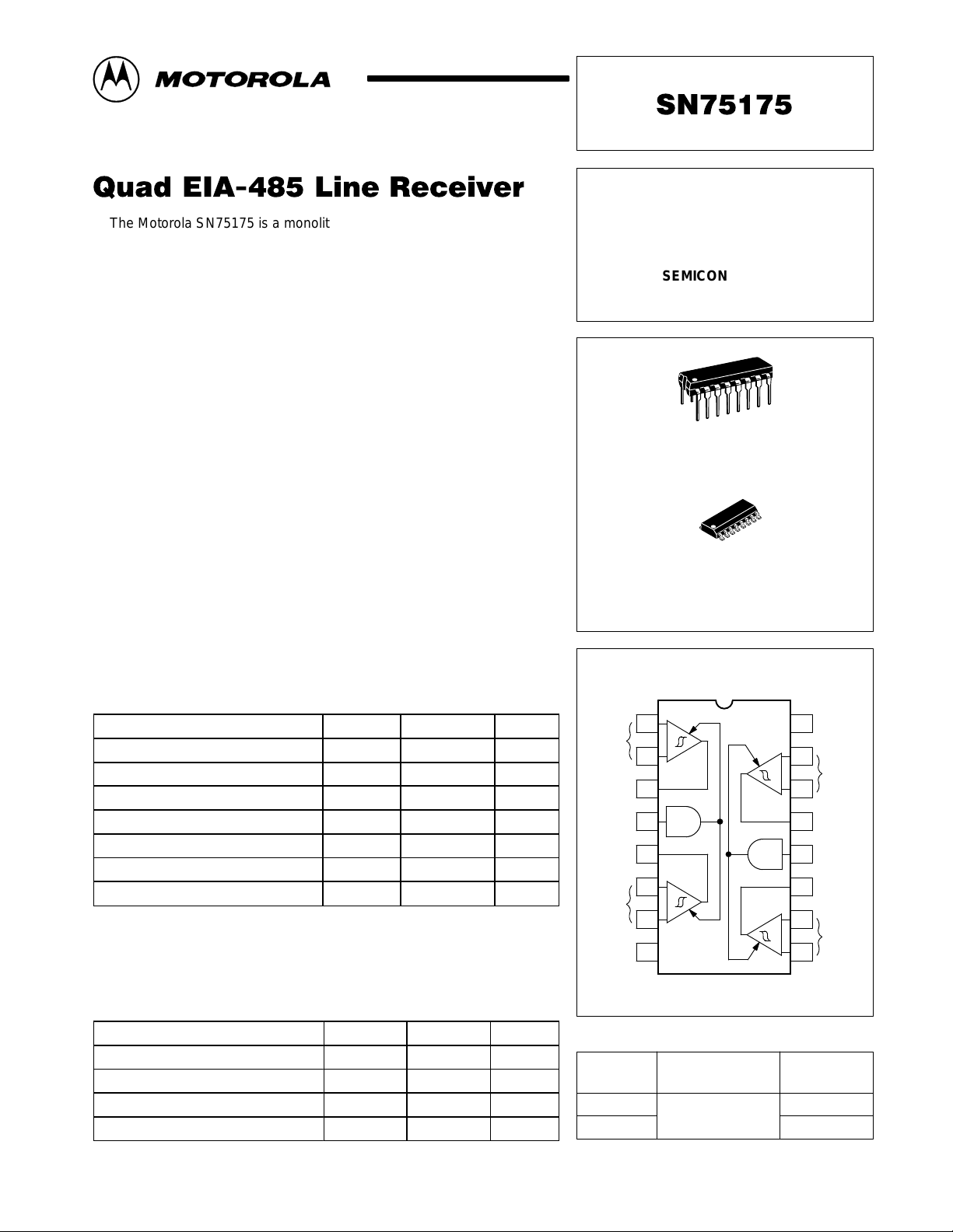
Order this document by SN75175/D
The Motorola SN75175 is a monolithic quad differential line receiver with
three–state outputs. It is designed specifically to meet the requirements of
EIA–485, EIA–422A/23A Standards and CCITT recommendations.
The device is optimized for balanced multipoint bus transmission at rates
up to 10 megabits per second. It also features high input impedance, input
hysteresis for increased noise immunity, and input sensitivity of ±200 mV
over a common mode input voltage range of –12 V to 12 V . The SN75175 is
designed for optimum performance when used with the SN75172 or
SN75174 quad differential line drivers.
• Meets EIA Standards EIA–422A and EIA–423A, EIA–485
• Meets CCITT Recommendations V.10, V.11, X.26, and X.27
• Designed for Multipoint Transmission on Long Bus Lines in Noisy
Environments
• 3–State Outputs
• Common–Mode Input Voltage Range . . . –12 V to 12 V
• Input Sensitivity . . . ±200 mV
• Input Hysteresis . . . 50 mV Typ
• High Input Impedance . . . 1 EIA–485 Unit Load
• Operates from Single 5.0 V Supply
• Lower Power Requirements
• Plug–In Replacement for MC3486
QUAD EIA–485
LINE RECEIVER WITH
THREE–STATE OUTPUTS
SEMICONDUCTOR
TECHNICAL DATA
16
1
N SUFFIX
PLASTIC PACKAGE
CASE 648
16
1
D SUFFIX
PLASTIC PACKAGE
CASE 751B
(SO–16)
This device contains 174 active transistors.
MAXIMUM RATINGS
Rating Symbol Value Unit
Power Supply Voltage V
Input Common Mode Voltage V
Input Differential Voltage V
Three–State Control Input Voltage V
Output Sink Current I
Storage Temperature T
Operating Junction Temperature T
NOTE: ESD data available upon request.
CC
ICM
ID
I
O
stg
J
RECOMMENDED OPERATING CONDITIONS
Rating Symbol Value Unit
Power Supply Voltage V
Operating Ambient Temperature T
Input Common Mode Voltage Range V
Input Differential Voltage Range V
CC
A
ICM
IDR
7.0 Vdc
±25 Vdc
±25 Vdc
7.0 Vdc
50 mA
–65 to +150 °C
+150 °C
4.75 to 5.25 Vdc
0 to +70 °C
–12 to +12 Vdc
–12 to +12 Vdc
Inputs
A
Output
A
3–State
Control
A/C
Output
C
Inputs
C
Gnd
Device
SN75175N
SN75175D
PIN CONNECTIONS
1
–
+
2
3
4
5
6
+
–
7
8
(Top View)
16
15
–
+
14
13
12
11
10
+
–
9
ORDERING INFORMATION
Operating
Temperature Range
TA = 0 to +70°C
Plastic DIP
V
CC
Inputs
B
Output
B
3–State
Control
B/D
Output
D
Inputs
D
Package
SO–16
MOTOROLA ANALOG IC DEVICE DATA
Motorola, Inc. 1996 Rev 0
1
SN75175
ELECTRICAL CHARACTERISTICS (Unless otherwise noted, minimum and maximum limits apply over recommended temperature and
power supply voltage ranges. Typical values are for TA = 25°C, VCC = 5.0 V, and V
Characteristic
Differential Input Threshold Voltage (Note 2)
(–12 V p V
(IO = –0.4 mA, VOH q 2.7 V)
(IO = 16 mA, VOL p 0.5 V)
Input Hysteresis VT+ – V
Input Line Current (Differential Inputs)
(Unmeasured Input at 0 V , Note 3)
(VI = 12 V)
(VI = –7.0 V)
Input Resistance (Note 4) r
Input Balance and Output Level (Note 3)
(–12 V pV
(IO = –0.4 mA, VID = 0.2 V)
(IO = 8.0 mA, VID = –0.2 V)
(IO = 16 mA, VID = –0.2 V)
Input Voltage – High Logic State (Three–State Control) V
Input Voltage – Low Logic State (Three–State Control) V
Input Current – High Logic State (Three–State Control)
(VIH = 2.7 V)
(VIH = 5.5 V)
Input Current – Low Logic State (Three–State Control)
(VIL = 0.4 V)
Input Clamp Diode Voltage (Three–State Control)
(IIK = –18 mA)
Output Third State Leakage Current
(V
= 3.0 V, VIL = 0.8 V, VO = 0.4 V)
I(D)
(V
= –3.0 V, VIL = 0.8 V, VO = 2.4 V)
I(D)
Output Short–Circuit Current (Note 5)
(V
= 3.0 V, VIH = 2.0 V, VO = 0 V)
I(D)
Power Supply Current (VIL = 0 V) (All Inputs Grounded) I
NOTES: 1. All currents into device pins are shown as positive, out of device pins are negative. All voltages referenced to ground unless otherwise noted.
2.Differential input threshold voltage and guaranteed output levels are done simultaneously for worst case.
3.Refer to EIA–485 for exact conditions. Input balance and guaranteed output levels are done simultaneously for worst case.
4.Input resistance should be derived from input line current specifications and is shown for reference only. See EIA–485 and input line current
specifications for more specific input resistance information.
5.Only one output at a time should be shorted.
p 12 V, VIH = 2.0 V)
ICM
p 12 V, VIH = 2.0 V)
ICM
Symbol Min Typ Max Unit
V
TH(D)
T–
I
I
i
V
OH
V
OL
V
OL
IH
IL
I
IH
I
IL
V
IK
I
OZ
I
OS
CC
= 0 V, Note 1.)
ICM
–
–
– 50 – mV
–
–
1 Unit
Load
2.7
–
–
2.0 – – V
– – 0.8 V
–
–
– – –100 µA
– – –1.5 V
–
–
–15 – –85 mA
– – 70 mA
–
–
–
–
– –
–
–
–
–
–
–
–
–0.2
–0.8
0.45
20
100
–20
0.2
1.0
–
0.5
20
V
mA
V
µA
µA
SWITCHING CHARACTERISTICS (Unless otherwise noted, V
Characteristic Symbol Min Typ Max Unit
Propagation Delay Time – Differential Inputs to Output
Output High to Low
Output Low to High
Propagation Delay Time – Three–State Control to Output
Output Low to Third State
Output High to Third State
Output Third State to High
Output Third State to Low
2
= 5.0 V and TA = 25°C.)
CC
t
PHL(D)
t
PLH(D)
t
PLZ
t
PHZ
t
PZH
t
PZL
–
–
–
–
–
–
25
25
16
19
11
11
35
35
35
35
30
30
ns
ns
MOTOROLA ANALOG IC DEVICE DATA
SN75175
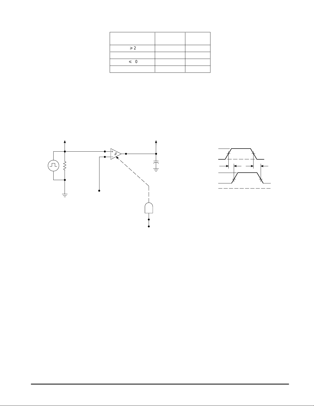
FUNCTION TABLE (EACH RECEIVER)
Differential Inputs Output
VIDq
2.0 V
–0.2 V<VID<0.2 V
VIDp
–0.2 V
XLZ
H = high level
L = low level
X = irrelevant
SWITCHING TEST CIRCUIT AND WAVEFORMS
Figure 1. Propagation Delay, Differential Input to Output
3–State
Control
HH
H?
HL
? = indeterminate
Z = high–impedance (off)
Y
Pulse
Generator
To Scope
(Input)
51
Differential
Inputs
1.5 V
2.0 V
3–State Control
To Scope
(Output)
(Includes Probe
Capacitance)
CL = 15 pF
and Stray
3.0 V
Input 1.5 V
0 V
t
PLH(D)
V
OH
V
OL
0 V
Input Pulse Characteristics –
t
= t
TLH
THL
PRR = 1.0 MHz, 50% Duty Cycle
1.5 V
Output
1.3 V
= 6.0 ns (10% to 90%)
t
PHL(D)
1.3 V
MOTOROLA ANALOG IC DEVICE DATA
3
 Loading...