

MOTOROLA SN74LS08ML2, SN74LS08MR1, SN74LS08N, SN74LS08DR2, SN74LS08M Datasheet
...
Semiconductor Components Industries, LLC, 1999
December, 1999 – Rev. 6
1 Publication Order Number:
SN74LS08/D
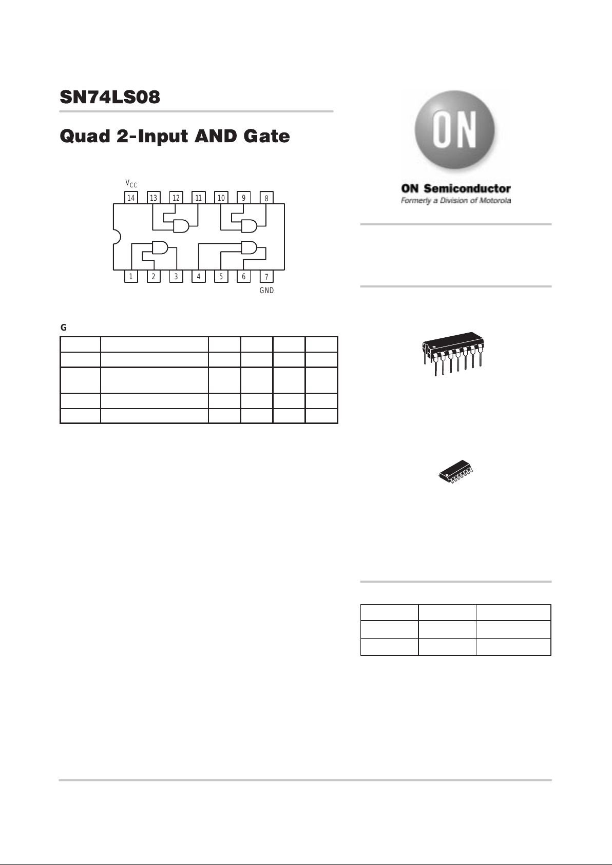
SN74LS08
Quad 2-Input AND Gate
14 13 12 11 10 9
123456
V
CC
8
7
GND
GUARANTEED OPERATING RANGES
Symbol Parameter Min Typ Max Unit
V
CC
Supply Voltage 4.75 5.0 5.25 V
T
A
Operating Ambient
T emperature Range
0 25 70 °C
I
OH
Output Current – High –0.4 mA
I
OL
Output Current – Low 8.0 mA
LOW
POWER
SCHOTTKY
SOIC
D SUFFIX
CASE 751A
http://onsemi.com
PLASTIC
N SUFFIX
CASE 646
14
1
14
1
Device Package Shipping
ORDERING INFORMATION
SN74LS08N 14 Pin DIP 2000 Units/Box
SN74LS08D 14 Pin
2500/Tape & Reel
SN74LS08
http://onsemi.com
2
DC CHARACTERISTICS OVER OPERATING TEMPERATURE RANGE (unless otherwise specified)
Limits
Symbol Parameter
Min Typ Max
Unit Test Conditions
V
IH
Input HIGH Voltage 2.0 V
Guaranteed Input HIGH Voltage for
All Inputs
V
IL
Input LOW Voltage
0.8
V
Guaranteed Input LOW Voltage for
All Inputs
V
IK
Input Clamp Diode Voltage –0.65 –1.5 V VCC = MIN, IIN = –18 mA
V
OH
Output HIGH Voltage
2.7 3.5 V VCC = MIN, IOH = MAX, VIN = V
IH
or VIL per Truth Table
p
0.25 0.4 V IOL = 4.0 mA
VCC = VCC MIN,
VOLOut ut LOW Voltage
0.35 0.5 V IOL = 8.0 mA
V
IN
=
V
IL
or
V
IH
per Truth Table
p
20 µA VCC = MAX, VIN = 2.7 V
IIHIn ut HIGH Current
0.1 mA VCC = MAX, VIN = 7.0 V
I
IL
Input LOW Current –0.4 mA VCC = MAX, VIN = 0.4 V
I
OS
Short Circuit Current (Note 1) –20 –100 mA VCC = MAX
Power Supply Current
I
CC
Total, Output HIGH
4.8
mA VCC = MAX
Total, Output LOW 8.8
Note 1: Not more than one output should be shorted at a time, nor for more than 1 second.
AC CHARACTERISTICS (TA = 25°C)
Limits
Symbol Parameter
Min Typ Max
Unit Test Conditions
t
PLH
Turn–Off Delay, Input to Output 8.0 15 ns
VCC = 5.0 V
t
PHL
Turn–On Delay, Input to Output 10 20 ns
CC
CL = 15 pF
 Loading...