

Motorola PZT2222AT1, PZT2222AT3 Datasheet
1
Motorola Small–Signal Transistors, FETs and Diodes Device Data
This NPN Silicon Epitaxial transistor is designed for use in linear and switching
applications. The device is housed in the SOT-223 package which is designed for
medium power surface mount applications.
• PNP Complement is PZT2907AT1
• The SOT-223 package can be soldered using wave or reflow.
• SOT-223 package ensures level mounting, resulting in improved thermal
conduction, and allows visual inspection of soldered joints. The formed
leads absorb thermal stress during soldering, eliminating the possibility of
damage to the die.
• Available in 12 mm tape and reel
Use PZT2222AT1 to order the 7 inch/1000 unit reel.
Use PZT2222AT3 to order the 13 inch/4000 unit reel.
MAXIMUM RATINGS
Rating Symbol Value Unit
Collector-Emitter Voltage V
CEO
40 Vdc
Collector-Base Voltage V
CBO
75 Vdc
Emitter-Base Voltage (Open Collector) V
EBO
6.0 Vdc
Collector Current I
C
600 mAdc
Total Power Dissipation up to TA = 25°C
(1)
P
D
1.5 Watts
Storage Temperature Range° T
stg
– 65 to +150 °C
Junction Temperature° T
J
150 °C
THERMAL CHARACTERISTICS
Thermal Resistance from Junction to Ambient R
θJA
83.3 °C/W
Lead Temperature for Soldering, 0.0625″ from case
Time in Solder Bath
T
L
260
10
°C
Sec
DEVICE MARKING
P1F
ELECTRICAL CHARACTERISTICS (T
A
= 25°C unless otherwise noted)
Characteristic
Symbol Min Max Unit
OFF CHARACTERISTICS
Collector-Emitter Breakdown Voltage (IC = 10 mAdc, IB = 0) V
(BR)CEO
40 — Vdc
Collector-Base Breakdown Voltage (IC = 10 µAdc, IE = 0) V
(BR)CBO
°75° °—° Vdc
Emitter-Base Breakdown Voltage (IE = 10 µAdc, IC = 0) V
(BR)EBO
6.0 — Vdc
Base-Emitter Cutoff Current (VCE = 60 Vdc, VBE = – 3.0 Vdc) I
BEX
— 20 nAdc
Collector-Emitter Cutoff Current (VCE = 60 Vdc, VBE = – 3.0 Vdc) I
CEX
— 10 nAdc
Emitter-Base Cutoff Current (VEB = 3.0 Vdc, IC = 0) I
EBO
— 100 nAdc
1. Device mounted on an epoxy printed circuit board 1.575 inches x 1 .575 inches x 0.059 inches; mounting pad for the collector lead min. 0.93 inches2.
Thermal Clad is a trademark of the Bergquist Company
Preferred devices are Motorola recommended choices for future use and best overall value.
Order this document
by PZT2222AT1/D
SEMICONDUCTOR TECHNICAL DATA
Motorola, Inc. 1996
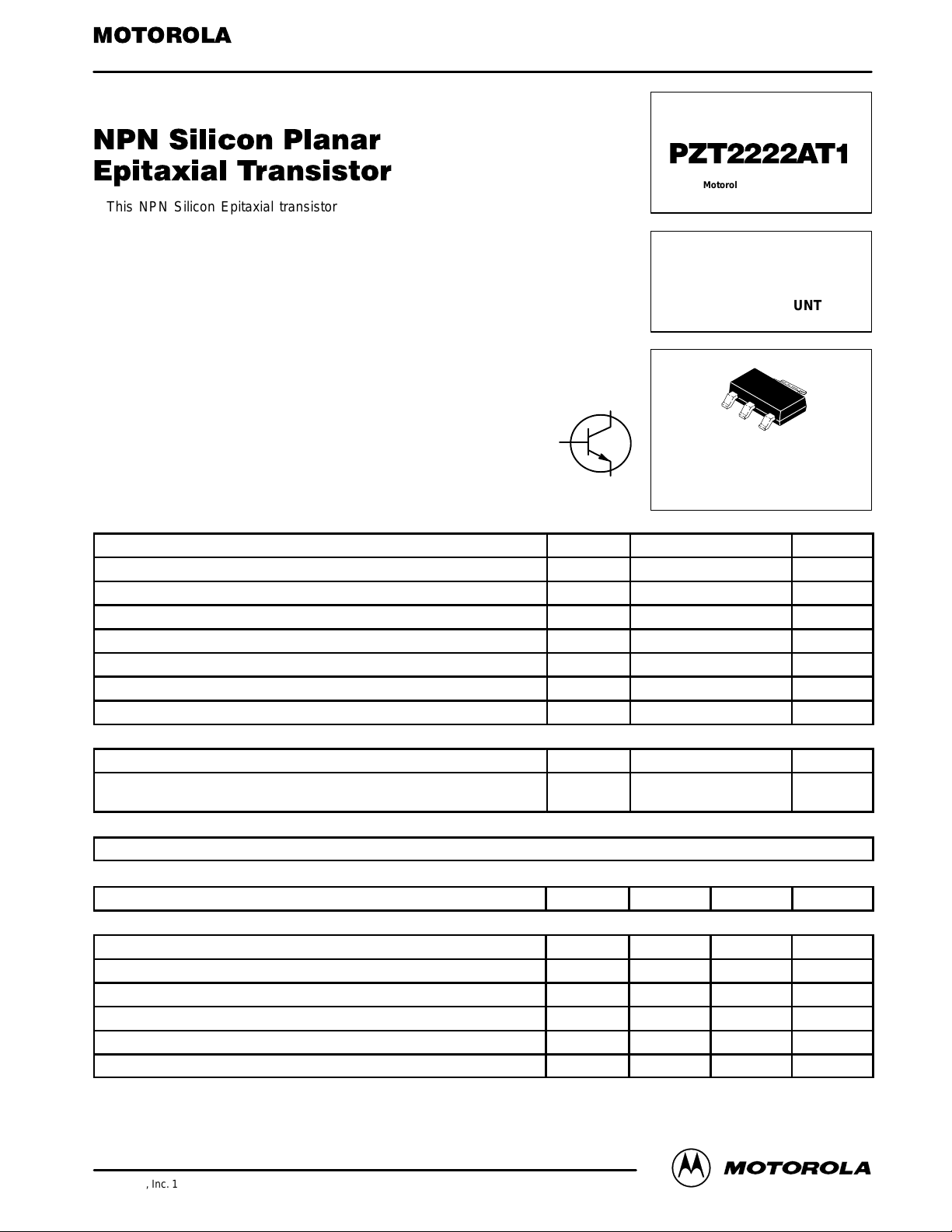
BASE
1
COLLECTOR
2, 4
3
EMITTER
SOT-223 PACKAGE
NPN SILICON
TRANSISTOR
SURFACE MOUNT
Motorola Preferred Device
CASE 318E-04, STYLE 1
TO-261AA
1
2
3
4
REV 2
PZT2222AT1
2
Motorola Small–Signal Transistors, FETs and Diodes Device Data
ELECTRICAL CHARACTERISTICS — continued
(TA = 25°C unless otherwise noted)
Characteristic
Symbol Min Max Unit
OFF CHARACTERISTICS (continued)
Collector-Base Cutoff Current
(VCB = 60 Vdc, IE = 0)
(VCB = 60 Vdc, IE = 0, TA = 125°C)
I
CBO
—
—
10
10
nAdc
µAdc
ON CHARACTERISTICS
DC Current Gain
(IC = 0.1 mAdc, VCE = 10 Vdc)
(IC = 1.0 mAdc, VCE = 10 Vdc)
(IC = 10 mAdc, VCE = 10 Vdc)
(IC = 10 mAdc, VCE = 10 Vdc, TA = – 55°C)
(IC = 150 mAdc, VCE = 10 Vdc)
(IC = 150 mAdc, VCE = 1.0 Vdc)
(IC = 500 mAdc, VCE = 10 Vdc)
h
FE
35
50
70
35
100
50
40
—
—
—
—
300
—
—
—
Collector-Emitter Saturation Voltages
(IC = 150 mAdc, IB = 15 mAdc)
(IC = 500 mAdc, IB = 50 mAdc)
V
CE(sat)
—
—
0.3
1.0
Vdc
Base-Emitter Saturation Voltages
(IC = 150 mAdc, IB = 15 mAdc)
(IC = 500 mAdc, IB = 50 mAdc)
V
BE(sat)
0.6
—
1.2
2.0
Vdc
Input Impedance°
(VCE = 10 Vdc, IC = 1.0 mAdc, f = 1.0 kHz)
(VCE = 10 Vdc, IC = 10 mAdc, f = 1.0 kHz)
°hie°
2.0
0.25
8.0
1.25
kΩ
Voltage Feedback Ratio
(VCE = 10 Vdc, IC = 1.0 mAdc, f = 1.0 kHz)
(VCE = 10 Vdc, IC = 10 mAdc, f = 1.0 kHz)
h
re
—
—
8.0x10
-4
4.0x10
-4
—
Small-Signal Current Gain
(VCE = 10 Vdc, IC = 1.0 mAdc, f = 1.0 kHz)
(VCE = 10 Vdc, IC = 10 mAdc, f = 1.0 kHz)
ť
hfeť
50
75
300
375
—
Output Admittance°
(VCE = 10 Vdc, IC = 1.0 mAdc, f = 1.0 kHz)
(VCE = 10 Vdc, IC = 10 mAdc, f = 1.0 kHz)
°hoe°
5.0
25
35
200
µmhos
Noise Figure (VCE = 10 Vdc, IC = 100 µAdc, f = 1.0 kHz) F — 4.0 dB
DYNAMIC CHARACTERISTICS
Current-Gain — Bandwidth Product
(IC = 20 mAdc, VCE = 20 Vdc, f = 100 MHz)
f
T
300 — MHz
Output Capacitance
(VCB = 10 Vdc, IE = 0, f = 1.0 MHz)
C
c
— 8.0 pF
Input Capacitance
(VEB = 0.5 Vdc, IC = 0, f = 1.0 MHz)
C
e
— 25 pF
SWITCHING TIMES (T
A
= 25°C)
Delay Time
t
d
— 10 ns
Rise Time
I
B(on)
= 15 mAdc, V
EB(off)
= 0.5 Vdc)
Figure 1
t
r
— 25
Storage Time
t
s
— 225 ns
Fall Time
I
B(on)
= I
B(off)
= 15 mAdc)
Figure 2
t
f
— 60
(VCC = 30 Vdc, IC = 150 mAdc,
(VCC = 30 Vdc, IC = 150 mAdc,
 Loading...