


查询MPC604E9VEC供应商
G522-0296-01
(IBM Order Number)
Advance Information
PowerPC
604e
™
RISC Microprocessor Family:
(Motorola Order Number)
MPC604E9VEC/D
5/97
REV 1
™
PID9v-604e Hardware Specifications
The PowerPC 604e microprocessor is an implementation of the PowerPC™ family of reduced
instruction set computing (RISC) microprocessors. In this document, the term ‘604’ is used as an
abbreviation for ‘PowerPC 604™ microprocessor’ and the term ‘604e’ is used as an abbreviation for
‘PowerPC 604e microprocessor’. The PowerPC 604e microprocessors are available from Motorola as
MPC604e and from IBM as PPC604e. This document contains pertinent physical characteristics of the
604e.
This document contains the following topics:
Topic Page
Section 1.1, “Overview” 2
Section 1.2, “Features” 2
Section 1.3, “General Parameters” 5
Section 1.4, “Electrical and Thermal Characteristics” 6
Section 1.5, “PowerPC 604e Microprocessor Pin Assignments” 17
Section 1.6, “PowerPC 604e Microprocessor Pinout Listings” 18
Section 1.7, “PowerPC 604e Microprocessor Package Description” 20
Section 1.8, “System Design Information” 22
Section 1.9, “Ordering Information 29
PRELIMINARY
T o locate any published errata or updates for this document, refer to the website at http://www .mot.com/
PowerPC/ or at http://www.chips.ibm.com/products/ppc.
The PowerPC name, the PowerPC logotype, PowerPC 604, and PowerPC 604e are trademarks
Corporation, used by Motorola under license from International Business Machines Corporation.
This document contains information on a new product under development by Motorola and IBM. Motorola and IBM reserve the right to
change or discontinue this product without notice.
Motorola Inc., 1997. All rights reserved.
©
Portions hereof
International Business Machines Corporation, 1991–1997. All rights reserved.
©
of International Business Machines
PID9v-604e Hardware Specifications

1.1 Overview
The 604e is an implementation of the PowerPC family of reduced instruction set computing (RISC)
microprocessors. The 604e implements the PowerPC architecture as it is specified for 32-bit addressing,
which provides 32-bit effective (logical) addresses, integer data types of 8, 16, and 32 bits, and floatingpoint data types of 32 and 64 bits (single-precision and double-precision). For 64-bit PowerPC
implementations, the PowerPC architecture provides additional 64-bit integer data types, 64-bit addressing,
and related features.
The 604e is a superscalar processor capable of issuing four instructions simultaneously. As many as seven
instructions can finish execution in parallel. The 604e has seven execution units that can operate in
parallel—a floating-point unit (FPU), a branch processing unit (BPU), a condition register unit (CRU), a
load/store unit (LSU), and three integer units (IUs)—two single-cycle integer units (SCIUs) and one
multiple-cycle integer unit (MCIU).
This parallel design, combined with the PowerPC architecture’s specification of uniform instructions that
allows for rapid execution times, yields high efficiency and throughput. The 604e’s rename buffers,
reservation stations, dynamic branch prediction, and completion unit increase instruction throughput,
guarantee in-order completion, and ensure a precise exception model. (Note that the PowerPC architecture
specification refers to all exceptions as interrupts.)
The 604e has separate memory management units (MMUs) and separate 32-Kbyte on-chip caches for
instructions and data. The 604e implements two 128-entry, two-way set associative translation lookaside
buffers (TLBs), one for instructions and one for data, and provides support for demand-paged virtual
memory address translation and variable-sized block translation. The TLBs and the cache use least-recently
used (LRU) replacement algorithms.
The 604e has a 64-bit external data bus and a 32-bit address bus. The 604e interface protocol allows multiple
masters to compete for system resources through a central external arbiter. Additionally, on-chip snooping
logic maintains data cache coherency for multiprocessor applications. The 604e supports single-beat and
burst data transfers for memory accesses and memory-mapped I/O accesses.
The 604e uses an advanced, 2.5-V CMOS process technology and is fully compatible with TTL devices.
1.2 Features
This section summarizes features of the 604e’s implementation of the Po werPC architecture. Major features
of the 604e are as follows:
• High-performance, superscalar microprocessor
— As many as four instructions can be issued per clock
— As many as seven instructions can start executing per clock (including three integer
instructions)
— Single-clock-cycle execution for most instructions
PRELIMINARY
• Seven independent execution units and two register files
— BPU featuring dynamic branch prediction
– Two-entry reservation station
– Out-of-order execution through two branches
– Shares dispatch bus with CRU
2 PID9v-604e Hardware Specifications
PRELIMINARY—SUBJECT TO CHANGE WITHOUT NOTICE

– 64-entry fully-associative branch target address cache (BTAC). In the 604e, the BTAC can
be disabled and invalidated.
– 512-entry branch history table (BHT) with two bits per entry for four levels of prediction—
not-taken, strongly not-taken, taken, strongly taken
— Condition register logical unit
– Two-entry reservation station
– Shares dispatch bus with BPU
— Two single-cycle IUs (SCIUs) and one multiple-cycle IU (MCIU)
– Instructions that execute in the SCIU take one cycle to execute; most instructions that
execute in the MCIU take multiple cycles to execute.
– Each SCIU has a two-entry reservation station to minimize stalls
– The MCIU has a single-entry reservation station and provides early exit (three c ycles) for
16- x 32-bit and overflow operations.
– Thirty-two GPRs for integer operands
— Three-stage floating-point unit (FPU)
– Fully IEEE 754-1985-compliant FPU for both single- and double-precision operations
– Supports non-IEEE mode for time-critical operations
– Fully pipelined, single-pass double-precision design
– Hardware support for denormalized numbers
– Two-entry reservation station to minimize stalls
– Thirty-two 64-bit FPRs for single- or double-precision operands
— Load/store unit (LSU)
– Two-entry reservation station to minimize stalls
– Single-cycle, pipelined cache access
– Dedicated adder performs effective address (EA) calculations
– Performs alignment and precision conversion for floating-point data
– Performs alignment and sign extension for integer data
– Four-entry finish load queue (FLQ) provides load miss buffering
– Six-entry store queue
– Supports both big- and little-endian modes
• Rename buffers
— Twelve GPR rename buffers
PRELIMINARY
— Eight FPR rename buffers
— Eight condition register (CR) rename buffers
• Completion unit
— The completion unit retires an instruction from the 16-entry reorder buffer when all instructions
ahead of it have been completed and the instruction has finished execution.
— Guarantees sequential programming model (precise exception model)
— Monitors all dispatched instructions and retires them in order
PID9v-604e Hardware Specifications 3
PRELIMINARY—SUBJECT TO CHANGE WITHOUT NOTICE

— Tracks unresolved branches and flushes e xecuted, dispatched, and fetched instructions if branch
is mispredicted
— Retires as many as four instructions per clock
• Separate on-chip instruction and data caches (Harvard architecture)
— 32-Kbyte, four-way set-associative instruction and data caches
— LRU replacement algorithm
— 32-byte (eight-word) cache block size
— Physically indexed/physical tags (Note that the PowerPC architecture refers to physical address
space as real address space.)
— Cache write-back or write-through operation programmable on a per page or per block basis
— Instruction cache can provide four instructions per clock; data cache can provide two words per
clock
— Caches can be disabled in software
— Caches can be locked
— Parity checking performed on both caches
— Data cache coherency (MESI) maintained in hardware
— Secondary data cache support provided
— Instruction cache coherency maintained in software
— Data cache line-fill buffer forwarding. In the 604 only the critical double word of the cache
block was made available to the requesting unit at the time it w as burst into the line-fill buffer.
Subsequent data was unavailable until the cache block w as filled. On the 604e, subsequent data
is also made available as it arrives in the line-fill buffer.
• Separate memory management units (MMUs) for instructions and data
— Address translation facilities for 4-Kbyte page size, variable block size, and 256-Mbyte
segment size
— Both TLBs are 128-entry and two-way set associative
— TLBs are hardware reloadable (that is, the page table search is performed in hardware)
— Separate IBATs and DBATs (four each) also defined as SPRs
— Separate instruction and data translation lookaside buffers (TLBs)
— LRU replacement algorithm
— 52-bit virtual address; 32-bit physical address
• Bus interface features
— Selectable processor-to-bus clock frequency ratios of 3:2, 2:1, 5:2, 3:1, 7:2, 4:1, 5:1, and 6:1
PRELIMINARY
— A 64-bit split-transaction external data bus with burst transfers
— Support for address pipelining and limited out-of-order bus transactions
— Four burst write queues—three for cache copyback operations and one for snoop push
operations
— Two single-beat write queues
— Additional signals and signal redefinition for direct-store operations
— Provides a data streaming mode that allows consecutive burst read data transfers to occur
without intervening dead cycles. This mode also disables data retry operations.
4 PID9v-604e Hardware Specifications
PRELIMINARY—SUBJECT TO CHANGE WITHOUT NOTICE

— No-DR
operations. This improves performance on read operations for systems that do not use the
DR
cycle sooner than if normal mode is used.
• Multiprocessing support features include the following:
— Hardware enforced, four-state cache coherency protocol (MESI) for data cache. Bits are
provided in the instruction cache to indicate only whether a cache block is valid or invalid.
— Separate port into data cache tags for bus snooping
— Load/store with reservation instruction pair for atomic memory references, semaphores, and
other multiprocessor operations
• Power management
— DOZE mode suspends instruction execution while allowing cache snooping
— NAP mode suspends all internal clocks except those required for decrementer, time base, and
interrupt logic
— Operating voltage of 2.5 ± 0.125 V
• Performance monitor can be used to help in debugging system designs and improving software
efficiency, especially in multiprocessor systems.
• In-system testability and debugging features through JTAG boundary-scan capability
TRY mode eliminates the DRTRY signal from the qualified bus grant and allows read
TRY signal. No-DRTRY mode makes read data available to the processor one bus clock
1.3 General Parameters
The following list provides a summary of the general parameters of the 604e:
Technology 0.35 µ m CMOS, five-layer metal
Die size 12.9 mm x 11.7 mm (148 mm
Transistor count 5.1 million
Logic design Fully-static
Package 255-lead ceramic ball grid array (CBGA)
Core power supply 2.5 V ± 5% V dc
I/O power supply 3.3 V ± 5% V dc
PRELIMINARY
2
)
PID9v-604e Hardware Specifications 5
PRELIMINARY—SUBJECT TO CHANGE WITHOUT NOTICE
° C
° C
1.4 Electrical and Thermal Characteristics
This section provides both the A C and DC electrical specifications and thermal characteristics for the 604e.
1.4.1 DC Electrical Characteristics
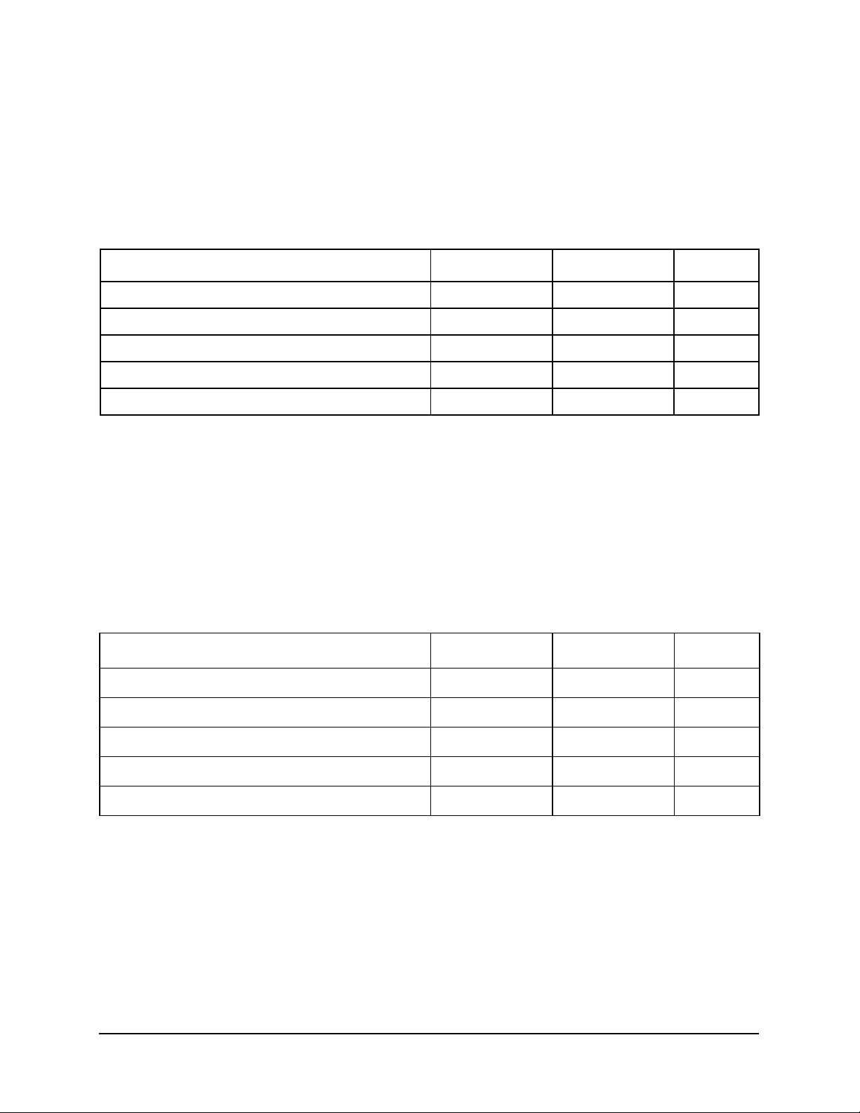
The tables in this section describe the 604e DC electrical characteristics. Table 1 provides the absolute
maximum ratings.
Table 1. Absolute Maximum Ratings
Characteristic Symbol Value Unit
Core supply voltage Vdd –0.3 to 2.75 V
PLL supply voltage AVdd –0.3 to 2.75 V
I/O supply voltage OVdd –0.3 to 3.6 V
Input voltage V
Storage temperature range T
Notes :
1. Functional and tested operating conditions are given in Table 2. Absolute maximum ratings are stress
ratings only, and functional operation at the maximums is not guaranteed. Stresses beyond those listed
may affect device reliability or cause permanent damage to the device.
2. Caution : V
3. Caution : OVdd must not exceed Vdd/AVdd by more than 1.2 V at any time including during power-on reset.
4. Caution : Vdd/AVdd must not exceed OVdd by more than 0.4 V at any time including during power-on reset.
must not exceed OVdd by more than 2.5 V at all times including during power-on reset.
in
in
stg
Table 2 provides the recommended operating conditions for the 604e.
Table 2. Recommended Operating Conditions
Characteristic Symbol Value Unit
–0.3 to 5.5 V
–55 to 150
PRELIMINARY
Core supply voltage Vdd 2.375 to 2.625 V
PLL supply voltage AVdd 2.375 to 2.625 V
I/O supply voltage OVdd 3.135 to 3.465 V
Input voltage V
in
GND to 5.5 V
Die-junction temperature T
Note: These are the recommended and tested operating conditions. Proper device operation outside of these
conditions is not guaranteed.
6 PID9v-604e Hardware Specifications
PRELIMINARY—SUBJECT TO CHANGE WITHOUT NOTICE
j
0 to 105
Table 3 provides the thermal characteristics for the 604e.
Table 3. Thermal Characteristics
Characteristic Symbol Value Rating
°
°
µ
µ
CBGA package thermal resistance, die junction-to-top-of-die (typical) θ
CBGA package thermal resistance, die junction-to-ball (typical) θ
Note: Refer to Section 1.8, “System Design Information,” for more details about thermal management.
JC
JB
0.1
3.8
Table 4 provides the DC electrical characteristics for the 604e.
Table 4. DC Electrical Specifications
Vdd = AVdd = 2.5 ± 5% V dc, OVdd = 3.3 ± 5% V dc, GND = 0 V dc, 0 ≤ Tj ≤ 105 ° C
Characteristic Symbol Min Max Unit
Input high voltage (all inputs except SYSCLK) V
Input low voltage (all inputs except SYSCLK) V
SYSCLK input high voltage CV
SYSCLK input low voltage CV
Input leakage current, V
Hi-Z (off-state) leakage current, V
Output high voltage, I
Output low voltage, I
Capacitance, V
and AR
Capacitance, V
AR
TRY)
TRY)
=
in
=
in
= 3.465 V
in
V
= 5.5 V
in
= –9
OH
mA V
9
=
OL
0 V, f = 1 MHz
PRELIMINARY
0 V, f = 1 MHz
1
1
3.465 V
=
in
=
V
in
mA V
2
(excludes TS
2
(for TS
1
1
5.5
V
, ABB, DBB,
, ABB, DBB, and
I
in
I
in
I
TSI
I
TSI
C
C
IH
IL
IH
IL
OH
OL
in
in
2.0 5.5 V
GND 0.8 V
2.4 5.5 V
GND 0.4 V
—10
— 245
—10
— 245
2.4 — V
— 0.4 V
— 10.0 pF
— 15.0 pF
C/W
C/W
µ
A
A
µ
A
A
Notes:
1. Excludes test signals (LSSD_MODE, L1_TSTCLK, L2_TSTCLK) and JTAG signals.
2. Capacitance values are guaranteed by design and characterization, and are not tested.
PID9v-604e Hardware Specifications 7
PRELIMINARY—SUBJECT TO CHANGE WITHOUT NOTICE
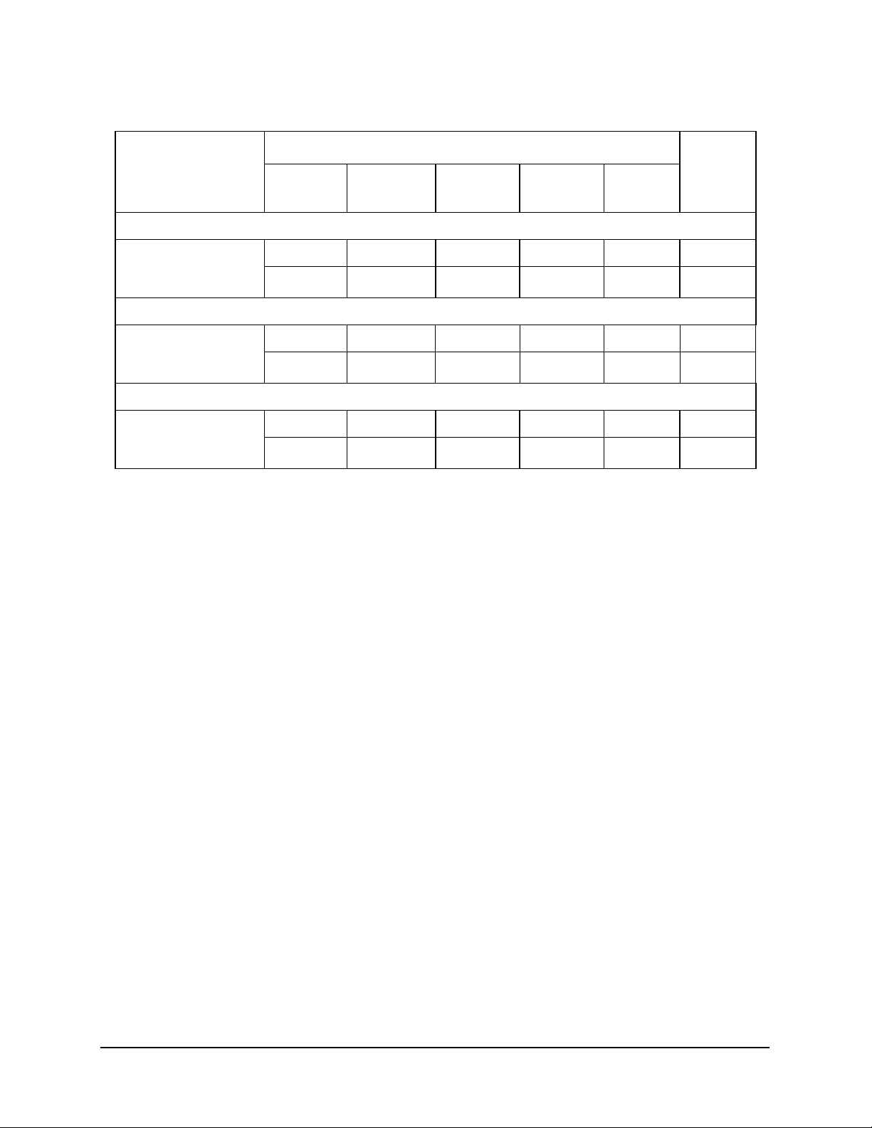
Table 5 provides the power consumption for the 604e.
Table 5. Power Consumption
Processor Core Frequency
CPU Clock:
SYSCLK
Full-On Mode
166
MHz
180
MHz
200
MHz
225
MHz
233
MHz
Unit
Typical
Maximum
Doze Mode
Typical
Maximum
Nap Mode
Typical
Maximum
Notes:
1. These values apply for all v alid PLL_CFG[0–3] settings and do not include output driver power (OVdd)
or analog supply power (AVdd). OVdd power is system dependent but is typically ≤ 10% of Vdd. Worstcase AVdd = 15 mW.
2. Typical power is an average value measured at Vdd = AVdd = 2.5 V, OVdd = 3.3 V, T
system executing typical applications and benchmark sequences. Typical power numbers should be
used in planning for proper thermal management.
3. Maximum power is measured at Vdd = AVdd = 2.625 V, OVdd = 3.465 V, T
instruction mix. These values should be used for power supply design.
12.4 13.5 14.5 15.9 16.7 W
13.3 14.3 15.7 17.4 18.0 W
1.1 1.1 1.1 1.1 1.2 W
1.2 1.2 1.3 1.3 1.3 W
0.8 0.8 0.9 0.9 0.9 W
1.1 1.1 1.1 1.1 1.1 W
= 25 °C in a
a
= 0 °C using a worst-case
j
1.4.2 AC Electrical Characteristics
PRELIMINARY
This section provides the AC electrical characteristics for the 604e. After fabrication, parts are sorted by
maximum processor core frequency as shown in Section 1.4.2.1, “Clock AC Specifications,” and tested for
conformance to the AC specifications for that frequency. These specifications are for 166.67, 180, 200, 225,
and 233 MHz processor core frequencies. The processor core frequency is determined by the bus
(SYSCLK) frequency and the settings of the PLL_CFG[0–3] signals. Parts are sold by maximum processor
core frequency; see Section 1.9, “Ordering Information.”
8 PID9v-604e Hardware Specifications
PRELIMINARY—SUBJECT TO CHANGE WITHOUT NOTICE

1.4.2.1 Clock AC Specifications
Table 6 provides the clock AC timing specifications as defined in Figure 1.
Table 6. Clock AC Timing Specifications
Vdd = AVdd = 2.5 ± 5% V dc, OVdd = 3.3 ± 5% V dc, GND = 0 V dc, 0 ≤ Tj ≤ 105 °C
166.67
Num Characteristic
Processor
frequency
VCO frequency 166 33 180 360 200 400 225 450 233 466 MHz 1
SYSCLK (bus)
frequency
1 SYSCLK cycle
time
2, 3 SYSCLK rise and
fall time
4 SYSCLK duty
cycle measured
at 1.4 V
SYSCLK jitter — ±150 — ±150 — ±150 ±150 ±150 ps 4
604e internal
PLL-relock time
Notes:
1. Caution: The SYSCLK frequency and PLL_CFG[0–3] settings must be chosen such that the resulting
SYSCLK (bus) frequency, CPU (core) frequency, and PLL (VCO) frequency do not exceed their respective
maximum or minimum operating frequencies. Refer to the PLL_CFG[0–3] signal description in Section 1.8,
“System Design Information,” for valid PLL_CFG[0–3] settings.
2. Rise and fall times for the SYSCLK input are measured from 0.4 V to 2.4 V.
3. Timing is guaranteed by design and characterization, and is not tested.
4. The total input jitter (short term and long term combined) must be under ±150 ps to guarantee the input and
output timing shown in Section 1.4.2.2, “Input AC Specifications” and Section 1.4.2.3, “Output AC
Specifications.”
5. PLL-relock time is the maximum time required for PLL lock after a stable Vdd, OVdd, AVdd, and SYSCLK
are reached during the power-on reset sequence. Also note that HRESET
minimum of 255 bus clocks after the PLL-relock time (100 µs) during the power-on reset sequence.
6. AC timing specifications are tested up to the maximum SYSCLK frequency shown here. However, it is
theoretically possible to attain higher SYSCLK frequencies, if allowed f or b y system design or by using 604e
Fast Out mode (see Table 11 for details).
MHz
Min Max Min Max Min Max Min Max Min Max
83.3 166.7 90 180 100 200 112 225 116 233 MHz 1
25 66 25 66 25 66 25 75 25 75 MHz 1, 6
15 40 15 40 15 40 13 40 13 40 ns
1.0 2.0 1.0 2.0 1.0 2.0 1.0 2.0 1.0 2.0 ns 2
40 60 40 60 40 60 40 60 40 60 % 3
— 100 — 100 — 100 100 100 µs 3, 5
PRELIMINARY
180
MHz
200
MHz
225
MHz
must be held asserted for a
233
MHz
Unit Notes
PID9v-604e Hardware Specifications 9
PRELIMINARY—SUBJECT TO CHANGE WITHOUT NOTICE

Figure 1 provides the SYSCLK input timing diagram.
1
4
2 34
CVih
SYSCLK
VM
CVil
VM = Midpoint Voltage (1.4 V)
Figure 1. SYSCLK Input Timing Diagram
1.4.2.2 Input AC Specifications
Table 7 provides the input AC timing specifications as defined in Figure 2 and Figure 3 for 604e processors
operating at 166.67, 180, 200, 225, and 233 MHz core frequencies.
Table 7. Input AC Timing Specifications, 166.67–233 MHz1
Vdd = AVdd = 2.5 ± 5% V dc, OVdd = 3.3 ± 5% V dc, GND = 0 V dc, 0 ≤ Tj ≤ 105 °C
166.67 MHz
Num Characteristic
Min Max Min Max
7a AR
7b All other inputs valid to SYSCLK (input setup) 2.25 — 2.0 — ns 2
TRY, SHD, ABB, TS, XATS, AACK, BG,
DR
TRY, T A, DBG, DBB, TEA, DBDIS , and DBW O
valid to SYSCLK (input setup)
3.5 — 3.25 — ns 2
180, 200, 225,
and 233 MHz
Unit Notes
8 SYSCLK to all inputs invalid (input hold) 0.5 — 0.5 — ns
9 Mode select input valid to HRESE
for DR
TRY)
10 HRESET
for DR
TRY)
Notes:
1. Input specifications are measured from the TTL level (0.8 or 2.0 V) of the signal in question to the 1.4 V of
the rising edge of the input SYSCLK. Input and output timings are measured at the pin (see Figure 2).
2. All other input signals include the following signals—all inputs except AR
AA
CK, BG, DRTRY, TA, DBG, DBB, DBWO, DBDIS, TEA, and JTAG inputs.
3. The setup and hold time is with respect to the rising edge of HRESET
4. t
5. These values are guaranteed by design, and are not tested.
6. Note this is for configuration of the fast-L2 mode and the no-DR
is the period of the external clock (SYSCLK) in nanoseconds.
sysclk
PRELIMINARY
to mode select input invalid (input hold
T (input setup
8 * t
sysclk
0 — 0 — ns 3, 4, 5, 6
— 8 * t
TRY, SHD, ABB, TS, XATS,
(see Figure 3).
TRY mode.
sysclk
— ns 3, 4, 5, 6
10 PID9v-604e Hardware Specifications
PRELIMINARY—SUBJECT TO CHANGE WITHOUT NOTICE

Figure 2 provides the input timing diagram for the 604e.
\
SYSCLK
7
ALL INPUTS
Figure 3 provides the mode select input timing diagram for the 604e.
HRESET
DRTRY
VM
8
VM = Midpoint Voltage (1.4 V)
Figure 2. Input Timing Diagram
VM
9
10
VM = Midpoint Voltage (1.4 V)
Figure 3. Mode Select Input Timing Diagram
1.4.2.3 Output AC Specifications
The output specifications of the 604e for both driving high and driving lo w depend on the capacitiv e loading
on each output and the drive capability enabled for that output. Additionally, the timing specifications for
outputs driving low also depend on the voltage swing required to drive to 0.8 V (either 5.5 V to 0.8 V or
3.6 V to 0.8 V). Table 8 provides the output A C timing specifications for a 50 pF load. In order to deri v e the
actual timing specifications for a given set of conditions, it is recommended that IBIS simulation models be
used. Contact the local Motorola or IBM sales office for information on the availability of these models.
The 604e adds a Fast Out output mode which will allow for increased system bus frequencies. Table 8
provides the output AC timing specifications for the 604e (shown in Figure 4) operating in 604
Compatibility mode and Fast Out mode. 604e Fast Out mode is selected by driving the L2_TSTCLK pin to
GND during assertion of HRESET
are reduced.
PRELIMINARY
. When Fast Out mode is enabled, the output v alid and output hold times
PID9v-604e Hardware Specifications 11
PRELIMINARY—SUBJECT TO CHANGE WITHOUT NOTICE

Table 8 provides the output AC timing specifications for 166.67, 180, 200, 225, and 233 MHz processors.
Table 8. Output AC Timing Specifications1
Vdd = AVdd = 2.5 ± 5% V dc, OVdd = 3.3 ± 5% V dc, GND = 0 V dc, CL = 50 pF, 0 ≤ Tj ≤ 105 °C, Drive mode [01]
166.67 MHz 180, 200, 225, and 233 MHz
Num Characteristic
Min Max
Fast Out
Min/Max
Min Max
Fast Out
Min/Max
7
Unit Notes
11 SYSCLK to output driven
(output enable time)
12a SYSCLK to TS, XATS,
AR
TRY, SHD, ABB and DBB
output valid (for 5.5 V to 0.8 V)
12b SYSCLK to TS
AR
TRY, SHD, ABB and DBB
output valid (for 3.6 V to 0.8 V)
13a SYSCLK to all other signals
output valid (for 5.5 V to 0.8 V)
13b SYSCLK to all other signals
output valid (for 3.6 V to 0.8 V)
14 SYSCLK to output invalid
(output hold)
15 SYSCLK to output high
impedance (all signals except
AR
TRY, SHD, ABB, DBB, TS,
and XA
TS)
16 SYSCLK to output high
impedance
17 SYSCLK to ABB
high impedance after
precharge
18 SYSCLK to AR
high impedance before
precharge
, XATS,
TS, XATS
and DBB
PRELIMINARY
TRY and SHD
0.75 — — 0.75 — — ns 2, 5
— 6.75 5.75 — 6.5 5.5 ns 3, 5
— 6.25 5.25 — 5.5 4.5 ns 5
— 7.75 6.75 — 7.5 6.5 ns 3, 5
— 7.25 6.25 — 6.5 5.5 ns 5
0.5 — 0.0 0.0 — 0.0 ns 2, 5
— 6.75 5.75 — 6.25 5.25 ns 5
— 6.75 5.75 — 6.25 5.25 ns 5
— 1.0*
t
— 6.75 5.75 — 6.25 5.25 ns 5
sysclk
1.0*
t
sysclk
— 1.0*
t
sysclk
1.0* t
sysclk
ns 4
19 SYSCLK to AR
precharge enable
20 Maximum delay to AR
and SHD
21 SYSCLK to AR
high impedance after
precharge
Rise time (AR
DBB
, TS, and XATS)
TRY, and SHD
precharge
TRY and SHD
TRY, SHD , ABB,
TRY
0.5*
t
+0.75
— 1.5*
— 2.0*
1.0 1.0 1.0 1.0 ns 6
— — 0.5*
sysclk
1.5* t
t
sysclk
2.0*
t
sysclk
t
sysclk
sysclk
— — ns 4
t
sysclk
+0.75
— 1.5*
t
sysclk
— 2.0*
t
sysclk
1.5* t
2.0* t
sysclk
sysclk
ns 4
ns 4
12 PID9v-604e Hardware Specifications
PRELIMINARY—SUBJECT TO CHANGE WITHOUT NOTICE

Table 8. Output AC Timing Specifications1 (Continued)
Vdd = AVdd = 2.5 ± 5% V dc, OVdd = 3.3 ± 5% V dc, GND = 0 V dc, CL = 50 pF, 0 ≤ Tj ≤ 105 °C, Drive mode [01]
166.67 MHz 180, 200, 225, and 233 MHz
Num Characteristic
Min Max
Fast Out
Min/Max
Min Max
Fast Out
Min/Max
7
Unit Notes
Rise time (all signals except
AR
TRY, SHD, ABB, DBB, TS,
and XA
TS)
Fall time (AR
DBB
, TS, and XATS)
Fall time (all signals except
AR
TRY, SHD, ABB, DBB, TS,
and XA
Notes:
1. All output specifications are measured from the 1.4 V of the rising edge of SYSCLK to the TTL lev el (0.8 V or
2.0 V) of the signal in question. Both input and output timings are measured at the pin (see Figure 4).
2. This minimum parameter assumes CL = 0 pF.
3. SYSCLK to output valid (5.5 V to 0.8 V) includes the extra delay associated with discharging the external
voltage from 5.5 V to 0.8 V instead of from 3.6 V to 0.8 V (5-V CMOS levels instead of 3.3-V CMOS levels).
4. t
5. Fast Out mode (L2_TSTCLK = GND) improves output valid timing and reduces output hold times. The 604e
6. These specifications are nominal values.
7. These timing specifications are tested with drive mode signals configured with DRVMODE0 = low,
is the period of the external bus clock (SYSCLK) in nanoseconds (ns). When the unit is given as t
sysclk
the numbers given in the table must be multiplied by the period of SYSCLK to compute the actual time
duration (in nanoseconds) of the parameter in question.
powers up in Compatibility mode in a 604 system (L2_TSTCLK = OVdd).
DRVMODE1 = high.
TRY, SHD, ABB,
TS)
1.0 1.0 1.0 1.0 ns 6
1.0 1.0 1.0 1.0 ns 6
1.0 1.0 1.0 1.0 ns 6
sysclk
PRELIMINARY
PID9v-604e Hardware Specifications 13
PRELIMINARY—SUBJECT TO CHANGE WITHOUT NOTICE

Figure 4 provides the output timing diagram for the 604e.
SYSCLK
ALL OUTPUTS
(Except TS
, ABB,
DBB
, ARTRY,
XA
TS, SHD)
TS, XATS
ABB, DBB
ARTRY, SHD
VM
13
11
12
VM
14
15
12
17
20
19
18
VM
14
16
21
VM = Midpoint Voltage (1.4 V)
Figure 4. PowerPC 604e Microprocessor Output Timing Diagram
PRELIMINARY
14 PID9v-604e Hardware Specifications
PRELIMINARY—SUBJECT TO CHANGE WITHOUT NOTICE

1.4.3 JTAG AC Timing Specifications
Table 9 provides the JTAG AC timing specifications as illustrated in Figure 5, Figure 6, Figure 7, and
Figure 8.
Table 9. JTAG AC Timing Specifications (Independent of SYSCLK)
Vdd = AVdd = 2.5 ± 5% V dc, OVdd = 3.3 ± 5%, GND = 0 V dc, CL = 50 pF, 0 ≤ Tj ≤ 105 °C
Num Characteristic Min Max Unit Notes
TCK frequency of operation 0 16 MHz
1 TCK cycle time 62.5 — ns
2 TCK clock pulse width measured at 1.5 V 25 — ns
3 TCK rise and fall times 0 3 ns
4 TRST
5 TRST
6 Boundary-scan input data setup time 0 — ns 2
7 Boundary-scan input data hold time 27 — ns 2
8 TCK to output data valid 4 25 ns 3
9 TCK to output high impedance 3 24 ns 3
10 TMS, TDI data setup time 0 — ns
11 TMS, TDI data hold time 25 — ns
12 TCK to TDO data valid 4 24 ns
13 TCK to TDO high impedance 3 15 ns
Notes:
1. TRST
2. Non-test signal input timing with respect to TCK.
3. Non-test signal output timing with respect to TCK.
setup time to TCK rising edge 13 — ns 1
assert time 40 — ns
PRELIMINARY
is an asynchronous signal. The setup time is for test purposes only.
Figure 5 provides the JTAG clock input timing diagram.
1
2
TCK
3
Figure 5. Clock Input Timing Diagram
PID9v-604e Hardware Specifications 15
PRELIMINARY—SUBJECT TO CHANGE WITHOUT NOTICE
3
VM = Midpoint Voltage (1.4 V)
VM
VM
2
VM

Figure 6 provides the TRST timing diagram.
TCK
TRST
5
Figure 6. TRST Timing Diagram
Figure 7 provides the boundary-scan timing diagram.
TCK
4
6 7
Data Inputs
8
Data Outputs
9
Data Outputs
8
Data Outputs
Figure 7. Boundary-Scan Timing Diagram
Figure 8 provides the test access port timing diagram.
TCK
TDI, TMS
PRELIMINARY
12
Input Data Valid
Output Data Valid
Output Data Valid
10 11
Input Data Valid
TDO
13
TDO
12
TDO
Figure 8. Test Access Port Timing Diagram
16 PID9v-604e Hardware Specifications
PRELIMINARY—SUBJECT TO CHANGE WITHOUT NOTICE
Output Data Valid
Output Data Valid

1.5 PowerPC 604e Microprocessor Pin Assignments
The following sections contain the pinout diagrams for the 604e. Note that the 604e is currently offered by
Motorola and IBM in a ceramic ball grid array (CBGA) package. The IBM and Motorola CBGA packages
have identical pinouts.
Figure 9 (in part A) shows the pinout of the CBGA package as viewed from the top surface. Part B shows
the side profile of the CBGA package to indicate the direction of the top surface view.
Part A
01 02 03 04 05 06 07 08 09 10 11 12 13 14 15 16
A
B
C
D
E
F
G
H
J
Part B
K
L
M
N
P
R
T
PRELIMINARY
Not to Scale
Substrate Assembly
Encapsulant
View
Die
Figure 9. Pinout of the CBGA Package as Viewed from the Top Surface
PID9v-604e Hardware Specifications 17
PRELIMINARY—SUBJECT TO CHANGE WITHOUT NOTICE

1.6 PowerPC 604e Microprocessor Pinout Listings
Table 10 provides the pinout listing for the 604e CBGA package.
Table 10. Pinout Listing for the CBGA Package
Signal Name Pin Number Active I/O
A[0–31] C16, E04, D13, F02, D14, G01, D15, E02, D16, D04, E13,
GO2, E15, H01, E16, H02, F13, J01, F14, J02, F15, H03,
F16, F04, G13, K01, G15, K02, H16, M01, J15, P01
CK L02 Low Input
AA
ABB
AP[0–3] C01, B04, B03, B02 High I/O
APE
ARRAY_WR
AR
TRY J04 Low I/O
AVDD A10 — —
BG
BR
CI
CKSTP_IN
CKSTP_OUT
CLK_OUT D07 — Output
CSE[0–1] B01, B05 High Output
1
K04 Low I/O
A04 Low Output
B07 Low Input
L01 Low Input
B06 Low Output
E01 Low Output
D08 Low Input
A06 Low Output
High I/O
DBB
DBG
DBDIS
DBW
O G04 Low Input
DH[0–31] P14, T16, R15, T15, R13, R12, P11, N11, R11,T12, T11,
DL[0–31] K13, K15, K16, L16, L15, L13, L14, M16, M15, M13, N16,
DP[0–7] M02, L03, N02, L04, R01, P02, M04, R02 High I/O
DPE
DR
TRY G16 Low Input
DRVMOD0
DRVMOD1
GBL
2
2
J14 Low I/O
N01 Low Input
PRELIMINARY
H15 Low Input
High I/O
R10, P09, N09, T10, R09, T09, P08, N08, R08, T08, N07,
R07, T07, P06, N06, R06, T06, R05, N05, T05, T04
High I/O
N15, N13, N14, P16, P15, R16, R14, T14, N10, P13, N12,
T13, P03, N03, N04, R03, T01, T02, P04, T03, R04
A05 Low Output
D05 Low Input
C03 High Input
F01 Low I/O
18 PID9v-604e Hardware Specifications
PRELIMINARY—SUBJECT TO CHANGE WITHOUT NOTICE

Table 10. Pinout Listing for the CBGA Package (Continued)
Signal Name Pin Number Active I/O
GND C05, C12, E03, E06, E08, E09, E11, E14, F05, F07, F10,
F12, G06, G08, G09, G11, H05, H07, H10, H12, J05, J07,
J10, J12, K06, K08, K09, K11, L05, L07, L10, L12, M03,
M06, M08, M09, M11, M14, P05, P12
HALTED B08 High Output
HRESET
INT
L1_TSTCLK
L2_INT D06 High Input
L2_TSTCLK
LSSD_MODE
MCP
OVDD C07, E05, E07, E10, E12, G03, G05, G12, G14, K03, K05,
PLL_CFG[0–3] A08, B09, A09, D09 High Input
RSR
V D01 Low Output
RUN C08 High Input
1
1
1
A07 Low Input
B15 Low Input
D11 Low Input
D12 Low Input
B10 Low Input
C13 Low Input
K12, K14, M05, M07, M10, M12, P07, P10
——
——
SHD
SMI
SRESET
SYSCLK C09 — Input
T
A H14 Low Input
H04 Low I/O
A16 Low Input
B14 Low Input
PRELIMINARY
TBEN C02 High Input
TBST
TC[0–2] A02, A03, C06 High Output
TCK C11 High Input
TDI A11 High Input
TDO A12 High Output
TEA
TMS B11 High Input
TRST
TS
TSIZ[0–2] A13, D10, B12 High I/O
A14 Low I/O
H13 Low Input
C10 Low Input
J13 Low I/O
TT[0–4] B13, A15, B16, C14, C15 High I/O
PID9v-604e Hardware Specifications 19
PRELIMINARY—SUBJECT TO CHANGE WITHOUT NOTICE

Table 10. Pinout Listing for the CBGA Package (Continued)
Signal Name Pin Number Active I/O
WT D02 Low Output
VDD F06, F08, F09, F11, G07, G10, H06, H08, H09, H11, J06,
J08, J09, J11, K07, K10, L06, L08, L09, L11
VOLTDETGND
XA
TS J16 Low I/O
3
NC
(No Connect)
Notes:
1. These are test signals for factory use only and must be pulled up to OVdd for normal machine operation.
2. To operate in accordance with these specifications, the drive mode signals must be DRVMODE0 = low,
DRVMODE1 = high
3. NC (no-connect) in the 604; internally tied to GND in the 604e CBGA package to indicate to the power
supply that a low-voltage processor is present.
3
F03 — —
C04, D03, J03
——
1.7 PowerPC 604e Microprocessor Package
Description
The following sections provide the package parameters and mechanical dimensions for the common IBM
and Motorola CBGA packages.
1.7.1 Package Parameters
The package parameters are as provided in the following list. The package type is 21 mm, 256-lead ceramic
ball grid array (CBGA).
Package outline 21 x 21 mm
Interconnects 255
Pitch 1.27 mm (50 mil)
Maximum module height 3.30 mm
Ball diameter 0.89 mm (35 mil)
PRELIMINARY
20 PID9v-604e Hardware Specifications
PRELIMINARY—SUBJECT TO CHANGE WITHOUT NOTICE

1.7.2 Mechanical Dimensions of the CBGA Package
Figure 10 provides the mechanical dimensions and bottom surface nomenclature of the IBM and Motorola
CBGA package.
2X
0.2
A1 CORNER
D
A
C
0.15 C
E
2X
0.2
B
12345678910111213141516
e/2
D1
PRELIMINARY
e
e/2
T
R
P
N
M
L
K
J
H
G
F
E
D
C
B
A
E1
NOTES:
1. DIMENSIONING AND TOLERANCING PER ASME Y14.5M, 1994.
2. DIMENSIONS IN MILLIMETERS.
3. TOP SIDE A1 CORNER INDEX IS A METALIZED FEATURE WITH
VARIOUS SHAPES. BOTTOM SIDE A1 CORNER IS
DESIGNATED WITH A BALL MISSING FROM THE ARRAY.
MILLIMETERS
DIM MIN MAX
2.65 3.20
A
A1 0.79 0.99
A2 1.10 1.30
A2
A1
A
b 0.82 0.93
D 21.00 BSC
D1 5.00 16.00
e 1.27 BSC
E 21.00 BSC
E1 5.00 16.00
255X
b
BC
A0.3
C
0.15
Figure 10. Mechanical Dimensions and Bottom Surface Nomenclature of the CBGA Package
PID9v-604e Hardware Specifications 21
PRELIMINARY—SUBJECT TO CHANGE WITHOUT NOTICE

1.8 System Design Information
This section provides electrical and thermal design recommendations for successful application of the 604e.
1.8.1 PLL Configuration
The 604e PLL is configured by the PLL_CFG[0–3] signals. For a given SYSCLK (b us) frequenc y, the PLL
configuration signals set the internal CPU and VCO frequency of operation. The PLL configuration for the
604e is shown in Table 11 for nominal frequencies.
Table 11. PowerPC 604e Microprocessor PLL Configuration
CPU Frequency in MHz (VCO Frequency in MHz)
PLL_CFG[0–3]
1100 1.5:1 x2 — — — — — 100
0100 2:1 x2 — — — 100
0110 2.5:1 x2 — — 100
1000 3:1 x2 — 100
1110 3.5:1 x2 — 116.6
1010 4:1 x2 100
1011 5:1 x2 125
1101 6:1 x2 150
0011 PLL bypass
CPU/
SYSCLK
Ratio
VCO
Multiplier
PRELIMINARY
Bus
25
MHz
(200)
(250)
(300)
Bus
33.3
MHz
(200)
(233)
133
(267)
166.5
(333)
200
(400)
Bus
40
MHz
(200)
120
(240)
140
(280)
160
(320)
200
(400)
———— —
Bus
50
MHz
120
(200)
125
(250)
150
(300)
175
(350)
200
(400)
——— —
(240)
150
(300)
180
(360)
210
(420)
—— —
Bus
60
MHz
Bus
66.6
MHz
(200)
133
(267)
166
(333)
200
(400)
233
(466)
Bus
75
MHz
112.5
(225)
150
(300)
187.5
(375)
225
(450)
—
1111 Clock off
Notes:
1. Some PLL configurations may select bus, CPU, or VCO frequencies which are not supported; see
Section 1.4.2.2, “Input AC Specifications,” for valid SYSCLK and VCO frequencies.
2. In PLL-bypass mode, the SYSCLK input signal clocks the internal processor directly, the PLL is disabled,
and the bus mode is set for 1:1 mode operation. This mode is intended for factory use only.
Note: The AC timing specifications given in this document do not apply in PLL-bypass mode.
22 PID9v-604e Hardware Specifications
PRELIMINARY—SUBJECT TO CHANGE WITHOUT NOTICE

1.8.2 PLL Power Supply Filtering
The AVdd po wer signal is provided on the 604e to provide po wer to the clock generation phase-locked loop.
T o ensure stability of the internal clock, the po wer supplied to the AVdd input signal should be filtered using
a circuit similar to the one shown in Figure 11. The circuit should be placed as close as possible to the AVdd
pin to ensure it filters out as much noise as possible.
10
Ω
Vdd A Vdd
(2.5 V)
Figure 11. PLL Power Supply Filter Circuit
10 µF 0.1 µF
GND
1.8.3 Decoupling Recommendations
Due to the 604e’s dynamic power management feature, large address and data buses, and high operating
frequencies, the 604e can generate transient power surges and high frequency noise in its power supply,
especially while driving large capacitive loads. This noise must be prevented from reaching other
components in the 604e system, and the 604e itself requires a clean, tightly regulated source of power.
Therefore, it is recommended that the system designer place at least one decoupling capacitor at each Vdd
and OVdd pin of the 604e. It is also recommended that these decoupling capacitors recei ve their po wer from
separate Vdd, OVdd, and GND power planes in the PCB, utilizing short traces to minimize inductance.
These capacitors should vary in value from 220 pF to 10 µF to provide both high- and low-frequency
filtering, and should be placed as close as possible to their associated Vdd or OVdd pin. Suggested values
for the Vdd pins—220 pF (ceramic), 0.01 µF (ceramic), and 0.1 µF (ceramic). Suggested values for the
OVdd pins—0.01 µF (ceramic), 0.1 µF (ceramic), and 10 µF (tantalum). Only SMT (surface mount
technology) capacitors should be used to minimize lead inductance.
In addition, it is recommended that there be several bulk storage capacitors distributed around the PCB,
feeding the Vdd and OVdd planes, to enable quick recharging of the smaller chip capacitors. These bulk
capacitors should also have a low ESR (equi valent series resistance) rating to ensure the quick response time
necessary. They should also be connected to the power and ground planes through two vias to minimize
inductance. The suggested values for these b ulk capacitors are 100 µF (AVX TPS tantalum) or 330 µF (AVX
TPS tantalum).
PRELIMINARY
1.8.4 Connection Recommendations
To ensure reliable operation, it is recommended to connect unused inputs to an appropriate signal level.
Unused active low inputs should be tied to Vdd. Unused active high inputs should be connected to GND.
1.8.5 Thermal Management Information
This section provides thermal management information for the ceramic ball grid array (CBGA) package in
air-cooled applications. Proper thermal control design is primarily dependent upon the system-level
design—the heat sink, airflow and thermal interface material. To reduce the die-junction temperature, a heat
sink may be attached to the package by several methods through the use of an adhesi ve, a spring clip to holes
in the printed-circuit board, or a mounting clip and screw assembly; see Figure 12. For applications where
the heat sink is attached by a spring clip, the spring force should not exceed 5.5 pounds of force.
PID9v-604e Hardware Specifications 23
PRELIMINARY—SUBJECT TO CHANGE WITHOUT NOTICE

Heat Sink
Heat Sink
Clip
Adhesive
or
Thermal Interface Material
CBGA Package
Printed-Circuit Board Option
Figure 12. Package Exploded Cross-Sectional View with Several Heat Sink Options
The board designer can choose between several types of heat sinks to place on the 604e. There are several
commercially-available heat sinks for the 604e provided by the following vendors:
Chip Coolers Inc. 800-227-0254 (USA/Canada)
333 Strawberry Field Rd. 401-739-7600
Warwick, RI 02887-6979
International Electronic Research Corporation (IERC) 818-842-7277
135 W. Magnolia Blvd.
Burbank, CA 91502
Thermalloy 214-243-4321
2021 W . Valley Vie w Lane
P.O. Box 810839
Dallas, TX 75731
Wakefield Engineering 617-245-5900
60 Audubon Rd.
Wakefield, MA 01880
Aavid Engineering 603-528-3400
One Kool Path
Laconia, NH 03247-0440
Ultimately, the final selection of an appropriate heat sink depends on many factors, such as thermal
performance at a given air velocity, spatial volume, mass, attachment method, assembly, and cost.
PRELIMINARY
24 PID9v-604e Hardware Specifications
PRELIMINARY—SUBJECT TO CHANGE WITHOUT NOTICE

1.8.5.1 Internal Package Conduction Resistance
For this packaging technology the intrinsic thermal conduction resistance (shown in Table 3) versus the
external thermal resistance paths are shown in Figure 13 for a package with an attached heat sink mounted
to a printed-circuit board.
External Resistance
Heat Sink
Internal Resistance
Printed-Circuit Board
External Resistance
(Note the internal versus external package resistance)
Figure 13. Package with Heat Sink Mounted to a Printed-Circuit Board
Radiation Convection
Thermal Interface Material
Die/Package
Die Junction
Package/Leads
Radiation Convection
1.8.5.2 Adhesives and Thermal Interface Materials
A thermal interface material is recommended at the package lid-to-heat sink interface to minimize the
thermal contact resistance. For those applications where the heat sink is attached by spring clip mechanism,
Figure 14 shows the thermal performance of three thin-sheet thermal-interface materials (silicone, graphite/
oil, floroether oil), a bare joint, and a joint with thermal grease as a function of contact pressure. As shown,
the performance of these thermal interface materials improves with increasing contact pressure. The use of
thermal grease significantly reduces the interface thermal resistance. That is, the bare joint results in a
thermal resistance approximately 7 times greater than the thermal grease joint.
PRELIMINARY
Therefore, the synthetic grease offers the best thermal performance, considering the low interface pressure.
Of course, the selection of any thermal interface material depends on many factors—thermal performance
requirements, manufacturability, service temperature, dielectric properties, cost, etc.
PID9v-604e Hardware Specifications 25
PRELIMINARY—SUBJECT TO CHANGE WITHOUT NOTICE

2
1.5
/W)
2
1
0.5
Specific Thermal Resistance (Kin
0
0 1020304050607080
Silicone Sheet (0.006 inch)
Bare Joint
Floroether Oil Sheet (0.007 inch)
Graphite/Oil Sheet (0.005 inch)
Synthetic Grease
Contact Pressure (psi)
Figure 14. Thermal Performance of Select Thermal Interface Material
The board designer can choose between several types of thermal interface. Heat sink adhesive materials
should be selected based upon high conductivity, yet adequate mechanical strength to meet equipment
shock/vibration requirements. There are several commercially-available thermal interfaces and adhesive
materials provided by the following vendors:
Dow-Corning Corporation 517-496-4000
Dow-Corning Electronic Materials
P.O. Box 0997
Midland, MI 48686-0997
Chomerics, Inc. 617-935-4850
77 Dragon Court
Woburn, MA 01888-4850
Thermagon Inc. 216-741-7659
3256 West 25th Street
Cleveland, OH 44109-1668
Loctite Corporation 860-571-5100
1001 Trout Brook Crossing
Rocky Hill, CT 06067
PRELIMINARY
26 PID9v-604e Hardware Specifications
PRELIMINARY—SUBJECT TO CHANGE WITHOUT NOTICE

AI Technology (e.g. EG7655) 609-882-2332
1425 Lower Ferry Rd.
Trent, NJ 08618
The following section provides a heat sink selection example using one of the commercially available heat
sinks.
1.8.5.3 Heat Sink Selection Example
For preliminary heat sink sizing, the die-junction temperature can be expressed as follows:
T
= Ta + Tr + (θjc + θ
j
Where:
is the die-junction temperature
T
j
is the inlet cabinet ambient temperature
T
a
is the air temperature rise within the electronic enclosure
T
r
is the die junction-to-case thermal resistance
θ
jc
is the adhesive or interface material thermal resistance
θ
int
is the heat sink base-to-ambient thermal resistance
θ
sa
is the power consumed by the device
P
d
During operation the die-junction temperatures (T
Table 2. The temperature of the air cooling the component greatly depends upon the ambient inlet air
temperature and the air temperature rise within the electronic enclosure. An electronic cabinet inlet-air
temperature (T
range of 5 to 10 °C. Assuming the thermal resistance of the thermal interf ace material (θ
1 °C/W, a T
following expression for T
) may range from 30 to 40 °C. The air temperature rise within a cabinet (Tr) may be in the
a
of 30 °C, a T
a
r
+ θsa) * Pd
int
) should be maintained less than the value specified in
j
) is typically about
int
of 5 °C a CBGA package θjc = 0.1, and a power consumption (Pd) of 15 W the
is obtained:
j
Die-junction temperature: T
For a Thermalloy heat sink #2328B, the heat sink-to-ambient thermal resistance (θ
is shown in Figure 15.
= 30 °C + 5 °C + (2.2 °C/W + 1.0 °C/W + θsa) * 15 W
j
PRELIMINARY
) versus airflow velocity
sa
PID9v-604e Hardware Specifications 27
PRELIMINARY—SUBJECT TO CHANGE WITHOUT NOTICE

8
7
6
5
4
3
Heat Sink Thermal Resistance (ºC/W)
2
1
0 0.5 1 1.5 2 2.5 3 3.5
Approach Air Velocity (m/s)
Figure 15. Thermalloy #2328B Heat Sink-to-Ambient Thermal Resistance Versus Airflow Velocity
Thermalloy #2328B Pin-fin Heat Sink
(25 x 28 x 15 mm)
Assuming an air velocity of 1 m/s, we have an effective θsa of 5 °C/W, thus
T
= 30 °C + 5 °C + (0.1 °C/W +1.0 °C/W + 5 °C/W) * 15 W,
j
resulting in a die-junction temperature of approximately 125 °C which exceeds the maximum operating
temperature of the component. To reduce the die junction temperature the designer has several options:
1. Increase the airflow velocity
2. Increase the surface area of the heat sink
3. Select a heat sink with an integrated cooling fan
Heat sinks offered by Chip Coolers, IERC, Thermalloy, Wakefield Engineering, and Aavid Engineering
offer different heat sink-to-ambient thermal resistances and air flow requirements.
Though the die junction-to-ambient and the heat sink-to-ambient thermal resistances are a common figureof-merit used for comparing the thermal performance of various microelectronic packaging technologies,
one should exercise caution when using only these metrics in determining thermal management because no
single parameter can adequately describe three-dimensional heat flow. The final die-junction operating
temperature is not only a function of the component-level thermal resistance, but the system-level design
and its operating conditions. In addition to the component's power consumption, a number of factors affect
the final operating die-junction temperature—airflow, board population (local heat flux of adjacent
components), heat sink efficiency, heat sink attach, heat sink placement, next-level interconnect technology ,
system air temperature rise, altitude, etc.
Due to the complexity and the many variations of system-level boundary conditions for today's
microelectronic equipment, the combined effects of the heat transfer mechanisms (radiation, con vection and
conduction) may vary widely. For these reasons, we recommend using conjugate heat transfer models for
PRELIMINARY
28 PID9v-604e Hardware Specifications
PRELIMINARY—SUBJECT TO CHANGE WITHOUT NOTICE

the board, as well as, system-level designs. To expedite system-level thermal analysis, several “compact”
thermal-package models are available within FLOTHERM®. These are available upon request.
1.9 Ordering Information
This section provides the part numbering nomenclature for the 604e. Note that the individual part numbers
correspond to a maximum processor core frequency . F or a v ailable frequencies, contact your local Motorola
or IBM sales office.
1.9.1 Motorola Part Number Key
Figure 16 provides the Motorola part numbering nomenclature for the 604e. In addition to the processor
frequency, the part numbering scheme also consists of a part modifier and application modifier. The part
modifier indicates any enhancement(s) in the part from the original production design. The application
modifier may specify special bus frequencies or application conditions. Each part number also contains a
revision code. This refers to the die mask re vision number and is specified in the part numbering scheme for
identification purposes only.
MPC 604 E XX XXX X X
Product Code
Part Identifier
Part Modifier
(E = Enhanced and Lower Voltage —604e)
Figure 16. Motorola Part Number Key
1.9.2 IBM Part Number Key
Figure 17 provides the IBM part numbering nomenclature for the 604e.
PRELIMINARY
PPC 604 e X X XXX
Product Code
Part Identifier
Part Modifier
(e = Enhanced and Lower Voltage)
Package
(B = BGA)
(Contact Local Motorola Sales Office)
Revision Level
Application Modifier
Processor Frequency
Package
(RX = BGA)
Processor Frequency
Revision Level
(Contact Local IBM Sales Office)
Figure 17. IBM Part Number Key
PID9v-604e Hardware Specifications 29
PRELIMINARY—SUBJECT TO CHANGE WITHOUT NOTICE

Information in this document is provided solely to enable system and software implementers to use PowerPC microprocessors. There are no express or
implied copyright or patent licenses granted hereunder by Motorola or IBM to design, modify the design of, or fabricate circuits based on the information in
this document.
The PowerPC 60x microprocessor embodies the intellectual property of Motorola and of IBM. However, neither Motorola nor IBM assumes any responsibility
or liability as to any aspects of the performance, operation, or other attributes of the microprocessor as marketed by the other party or by any third party. Neither
Motorola nor IBM is to be considered an agent or representative of the other party or any third party, and neither has assumed, created, or granted hereby any
right or authority to the other, or to any third party, to assume or create any express or implied obligations on its behalf. Information such as errata sheets and
data sheets, as well as sales terms and conditions such as prices, schedules, and support, for the product may vary as between parties selling the product.
Accordingly, customers wishing to learn more information about the products as marketed by a given party should contact that party.
Both Motorola and IBM reserve the right to modify this document and/or any of the products as described herein without further notice. NOTHING IN THIS
DOCUMENT, NOR IN ANY OF THE ERRATA SHEETS, DATA SHEETS, AND O THER SUPPORTING DOCUMENTATION, SHALL BE INTERPRETED AS THE
CONVEYANCE BY MOTOROLA OR IBM OF AN EXPRESS WARRANTY OF ANY KIND OR IMPLIED WARRANTY, REPRESENTATION, OR GUARANTEE
REGARDING THE MERCHANTABILITY OR FITNESS OF THE PRODUCTS FOR ANY PARTICULAR PURPOSE. Neither Motorola nor IBM assumes any
liability or obligation for damages of any kind arising out of the application or use of these materials. Any w arranty or other obligations as to the products described
herein shall be undertaken solely by the marketing party to the customer, under a separate sale agreement between the marketing party and the customer. In the
absence of such an agreement, no liability is assumed by Motorola, IBM, or the marketing party for any damages, actual or otherwise.
“Typical” parameters can and do vary in different applications. All operating parameters, including “Typicals,” m ust be v alidated f or each customer application b y
customer’s technical experts. Neither Motorola nor IBM convey any license under their respective intellectual property rights nor the rights of others. Neither
Motorola nor IBM makes any claim, warranty, or representation, express or implied, that the products described in this document are designed, intended, or
authorized for use as components in systems intended for surgical implant into the body, or other applications intended to support or sustain life, or for any other
application in which the failure of the product could create a situation where personal injury or death may occur. Should customer purchase or use the products
for any such unintended or unauthorized application, customer shall indemnify and hold Motorola and IBM and their respective officers, employees, subsidiaries,
affiliates, and distributors harmless against all claims, costs, damages, and expenses, and reasonab le attorney’ s fees arising out of, directly or indirectly, any claim
of personal injury or death associated with such unintended or unauthorized use, even if such claim alleges that Motorola or IBM was negligent regarding the
design or manufacture of the part.
Motorola and are registered trademarks of Motorola, Inc. Mfax is a trademark of Motorola, Inc. Motorola, Inc. is an Equal Opportunity/Affir mative Action
Employer.
IBM, the IBM logo, and IBM Microelectronics are trademarks of International Business Machines Corporation.
The PowerPC name, the P ow erPC logotype, P owerPC 604, and P owerPC 604e are trademarks of International Business Machines Corporation, used by Motorola
under license from International Business Machines Corporation. International Business Machines Corporation is an Equal Opportunity/Affir mative Action
Employer.
International Business Machines Corporation:
IBM Microelectronics Division, 1580 Route 52, Bldg. 504, Hopewell
Junction, NY 12533-6531; Tel. (800) PowerPC
World Wide Web Address: http://www.chips.ibm.com/products/ppc
http://www.ibm.com
Motorola Literature Distribution Centers:
USA/EUROPE: Motorola Literature Distribution; P.O. Box 5405; Denver, Colorado 80217;
Tel.: 1-800-441-2447 or (303) 675-2140
JAPAN: Nippon Motorola Ltd SPD, Strategic Planning Office 4-32-1, Nishi- Gotanda
Shinagawa-ku, Tokyo 141, Japan Tel.: 81-3-5487-8488
ASIA/PACIFC: Motorola Semiconductors H.K. Ltd.; 8B Tai Ping Industrial Park, 51 Ting
Kok Road, Tai Po, N.T., Hong Kong; Tel.: 852-26629298
Mfax™: RMFAX0@email.sps.mot.com; TOUCHTONE (602) 244-6609; US & Canada
ONLY (800) 774-1848
INTERNET: http://motorola.com/sps
Technical Information: Motorola Inc. SPS Customer Support Center; (800) 521-6274.
Document Comments: FAX (512) 891-2638, Attn: RISC Applications Engineering.
World Wide Web Address: http://www.mot.com/powerpc/
MPC604E9VEC/D
 Loading...