

Page 1

查询MPC604E9QEC供应商
G522-0319-00
(IBM Order Number)
MPC604E9QEC/D
(Motorola Order Number)
3/98
ª
Advance Information
PowerPC
604e
ª
RISC Microprocessor Family:
PID9q-604e Hardware SpeciÞcations
The PowerPC 604e microprocessor is an implementation of the PowerPC¨ family of reduced
instruction set computing (RISC) microprocessors. In this document, the term Ô604Õ is used as an
abbreviation for ÔPowerPC 604ª microprocessorÕ and the term Ô604eÕ is used as an abbreviation for
ÔPowerPC 604e microprocessorÕ. The PowerPC 604e microprocessors are available from Motorola as
MPC604e and from IBM as PPC604e. When ordering, note that PID9q-604e processors prior to
revision 1.1 are referenced as the PID10q-604e. This document contains pertinent physical
characteristics of the 604e.
This document contains the following topics:
Topic Page
Section 1.1, ÒOverviewÓ 2
Section 1.2, ÒFeaturesÓ 2
Section 1.3, ÒGeneral ParametersÓ 5
Section 1.4, ÒElectrical and Thermal CharacteristicsÓ 6
Section 1.5, ÒPin AssignmentsÓ 16
Section 1.6, ÒPinout ListingsÓ 17
Section 1.7, ÒPackage DescriptionÓ 19
Section 1.8, ÒSystem Design InformationÓ 20
Section 1.9, ÒOrdering Information 27
PRELIMINARY
To locate any published errata or updates for this document, refer to the website at http://www.mot.com/
SPS/PowerPC/ or at http://www.chips.ibm.com/products/ppc.
The PowerPC name is a registered trademark and the PowerPC logotype, PowerPC 604 and PowerPC 604e are trademarks
Machines Corporation, used by Motorola under license from International Business Machines Corporation. FLOTHERM is a registered trademark of
Flomerics Ltd., UK.
This document contains information on a new product under development by Motorola and IBM. Motorola and IBM reserve the right to
discontinue this product without notice.
Motorola Inc., 1997. All rights reserved.
©
Portions hereof
International Business Machines Corporation, 1991Ð1997. All rights reserved.
©
of International Business
change or
PID9q-604e Hardware Specifications
Page 2

1.1 Overview
The 604e is an implementation of the PowerPC family of reduced instruction set computing (RISC)
microprocessors. The 604e implements the PowerPC architecture as it is speciÞed for 32-bit addressing,
which provides 32-bit effective (logical) addresses, integer data types of 8, 16, and 32 bits, and ßoatingpoint data types of 32 and 64 bits (single-precision and double-precision). For 64-bit PowerPC
implementations, the PowerPC architecture provides additional 64-bit integer data types, 64-bit addressing,
and related features.
The 604e is a superscalar processor capable of issuing four instructions simultaneously. As many as seven
instructions can Þnish execution in parallel. The 604e has seven execution units that can operate in
parallelÑa ßoating-point unit (FPU), a branch processing unit (BPU), a condition register unit (CRU), a
load/store unit (LSU), and three integer units (IUs)Ñtwo single-cycle integer units (SCIUs) and one
multiple-cycle integer unit (MCIU).
This parallel design, combined with the PowerPC architectureÕs speciÞcation of uniform instructions that
allows for rapid execution times, yields high efÞciency and throughput. The 604eÕs rename buffers,
reservation stations, dynamic branch prediction, and completion unit increase instruction throughput,
guarantee in-order completion, and ensure a precise exception model. (Note that the PowerPC architecture
speciÞcation refers to all exceptions as interrupts.)
The 604e has separate memory management units (MMUs) and separate 32-Kbyte on-chip caches for
instructions and data. The 604e implements two 128-entry, two-way set associative translation lookaside
buffers (TLBs), one for instructions and one for data, and provides support for demand-paged virtual
memory address translation and variable-sized block translation. The TLBs and the cache use least-recently
used (LRU) replacement algorithms.
The 604e has a 64-bit external data bus and a 32-bit address bus. The 604e interface protocol allows multiple
masters to compete for system resources through a central external arbiter. Additionally, on-chip snooping
logic maintains data cache coherency for multiprocessor applications. The 604e supports single-beat and
burst data transfers for memory accesses and memory-mapped I/O accesses.
The 604e uses an advanced, 1.9V CMOS process technology and is fully compatible with 3.3V TTL
devices.
PRELIMINARY
1.2 Features
This section summarizes features of the 604eÕs implementation of the PowerPC architecture. Major features
of the 604e are as follows:
¥ High-performance, superscalar microprocessor
Ñ As many as four instructions can be issued per clock
Ñ As many as seven instructions can start executing per clock (including three integer
instructions)
Ñ Single-clock-cycle execution for most instructions
2 PID9q-604e Hardware Specifications
PRELIMINARYÑSUBJECT TO CHANGE WITHOUT NOTICE
Page 3

¥ Seven independent execution units and two register Þles
Ñ BPU featuring dynamic branch prediction
Ð Two-entry reservation station
Ð Out-of-order execution through two branches
Ð Shares dispatch bus with CRU
Ð 64-entry fully-associative branch target address cache (BTAC). In the 604e, the BTAC can
be disabled and invalidated.
Ð 512-entry branch history table (BHT) with two bits per entry for four levels of predictionÑ
not-taken, strongly not-taken, taken, strongly taken
Ñ Condition register logical unit
Ð Two-entry reservation station
Ð Shares dispatch bus with BPU
Ñ Two single-cycle IUs (SCIUs) and one multiple-cycle IU (MCIU)
Ð Instructions that execute in the SCIU take one cycle to execute; most instructions that
execute in the MCIU take multiple cycles to execute.
Ð Each SCIU has a two-entry reservation station to minimize stalls
Ð The MCIU has a single-entry reservation station and provides early exit (three cycles) for
16- x 32-bit and overßow operations.
Ð Thirty-two GPRs for integer operands
Ñ Three-stage ßoating-point unit (FPU)
Ð Fully IEEE 754-1985-compliant FPU for both single- and double-precision operations
Ð Supports non-IEEE mode for time-critical operations
Ð Fully pipelined, single-pass double-precision design
Ð Hardware support for denormalized numbers
Ð Two-entry reservation station to minimize stalls
Ð Thirty-two 64-bit FPRs for single- or double-precision operands
Ñ Load/store unit (LSU)
Ð Two-entry reservation station to minimize stalls
Ð Single-cycle, pipelined cache access
Ð Dedicated adder performs effective address (EA) calculations
Ð Performs alignment and precision conversion for ßoating-point data
Ð Performs alignment and sign extension for integer data
Ð Four-entry Þnish load queue (FLQ) provides load miss buffering
PRELIMINARY
Ð Six-entry store queue
Ð Supports both big- and little-endian modes
¥ Rename buffers
Ñ Twelve GPR rename buffers
Ñ Eight FPR rename buffers
Ñ Eight condition register (CR) rename buffers
PID9q-604e Hardware Specifications 3
PRELIMINARYÑSUBJECT TO CHANGE WITHOUT NOTICE
Page 4

¥ Completion unit
Ñ The completion unit retires an instruction from the 16-entry reorder buffer when all instructions
ahead of it have been completed and the instruction has Þnished execution.
Ñ Guarantees sequential programming model (precise exception model)
Ñ Monitors all dispatched instructions and retires them in order
Ñ Tracks unresolved branches and ßushes executed, dispatched, and fetched instructions if branch
is mispredicted
Ñ Retires as many as four instructions per clock
¥ Separate on-chip instruction and data caches (Harvard architecture)
Ñ 32-Kbyte, four-way set-associative instruction and data caches
Ñ LRU replacement algorithm
Ñ 32-byte (eight-word) cache block size
Ñ Physically indexed/physical tags. (Note that the PowerPC architecture refers to physical
address space as real address space.)
Ñ Cache write-back or write-through operation programmable on a per page or per block basis
Ñ Instruction cache can provide four instructions per clock; data cache can provide two words per
clock
Ñ Caches can be disabled in software
Ñ Caches can be locked
Ñ Parity checking performed on both caches
Ñ Data cache coherency (MESI) maintained in hardware
Ñ Secondary data cache support provided
Ñ Instruction cache coherency maintained in hardware
Ñ Data cache line-Þll buffer forwarding. In the 604 only the critical double word of the cache
block was made available to the requesting unit at the time it was burst into the line-Þll buffer.
Subsequent data was unavailable until the cache block was Þlled. On the 604e, subsequent data
is also made available as it arrives in the line-Þll buffer.
¥ Separate memory management units (MMUs) for instructions and data
Ñ Address translation facilities for 4-Kbyte page size, variable block size, and 256-Mbyte
segment size
Ñ Both TLBs are 128-entry and two-way set associative
Ñ TLBs are hardware reloadable (that is, the page table search is performed in hardware)
Ñ Separate IBATs and DBATs (four each) also deÞned as SPRs
Ñ Separate instruction and data translation lookaside buffers (TLBs)
Ñ LRU replacement algorithm
PRELIMINARY
Ñ 52-bit virtual address; 32-bit physical address
¥ Bus interface features include the following:
Ñ Selectable processor-to-bus clock frequency ratios (1:1, 3:2, 2:1, 5:2, 3:1, 7:2, 4:1, 9:2, 5:1,
11:2, 6:1, 13:2, and 7:1)
Ñ A 64-bit split-transaction external data bus with burst transfers
Ñ Support for address pipelining and limited out-of-order bus transactions
4 PID9q-604e Hardware Specifications
PRELIMINARYÑSUBJECT TO CHANGE WITHOUT NOTICE
Page 5

Ñ Four burst write queuesÑthree for cache copyback operations and one for snoop push
operations
Ñ Two single-beat write queues
Ñ Additional signals and signal redeÞnition for direct-store operations
Ñ Provides a data streaming mode that allows consecutive burst read data transfers to occur
without intervening dead cycles. This mode also disables data retry operations.
Ñ No-DR
operations. This improves performance on read operations for systems that do not use the
DR
cycle sooner than if normal mode is used.
¥ Multiprocessing support features include the following:
Ñ Hardware enforced, four-state cache coherency protocol (MESI) for data cache. Bits are
provided in the instruction cache to indicate only whether a cache block is valid or invalid.
Ñ Separate port into data cache tags for bus snooping
Ñ Load/store with reservation instruction pair for atomic memory references, semaphores, and
other multiprocessor operations
¥ Power management
Ñ NAP mode supports full shut down and snooping
Ñ Operating voltage of 1.9 ± 100 mV
¥ Performance monitor can be used to help in debugging system designs and improving software
efÞciency, especially in multiprocessor systems.
¥ In-system testability and debugging features through JTAG boundary-scan capability
TRY mode eliminates the DRTRY signal from the qualiÞed bus grant and allows read
TRY signal. No-DRTRY mode makes read data available to the processor one bus clock
1.3 General Parameters
The following list provides a summary of the general parameters of the 604e:
Technology 0.25 µm CMOS, Þve-layer metal
Die size 6.97 mm x 6.75mm (47 mm
Transistor count 5.1 million
Logic design Fully-static
Package Surface mount 255-lead ceramic ball grid array (CBGA)
Core power supply 1.9 V ± 100 mV dc
I/O power supply 3.3 V ± 5% V dc
PRELIMINARY
2
)
PID9q-604e Hardware Specifications 5
PRELIMINARYÑSUBJECT TO CHANGE WITHOUT NOTICE
Page 6
£
1.4 Electrical and Thermal Characteristics
This section provides both the AC and DC electrical speciÞcations and thermal characteristics for the 604e.
1.4.1 DC Electrical Characteristics
The tables in this section describe the 604e DC electrical characteristics. Table 1 provides the absolute
maximum ratings.
Table 1. Absolute Maximum Ratings
Characteristic Symbol Value Unit
Core supply voltage Vdd Ð0.3 to 2.80 V
PLL supply voltage AVdd Ð0.3 to 2.80 V
I/O supply voltage OVdd Ð0.3 to 3.8 V
Input voltage V
Overshoot (with respect to system GND) V
Undershoot (with respect to system GND) V
Storage temperature range T
Notes :
1. Functional and tested operating conditions are given in Table 2. Absolute maximum ratings are stress
ratings only, and functional operation at the maximums is not guaranteed. Stresses beyond those listed
may affect device reliability or cause permanent damage to the device.
Caution : Power up/down sequence must be adhered to to avoid device damage.
2.
¥ The power-up sequence is GND, Vdd, OVdd
¥ The power-down sequence is OVdd, Vdd, GND
In either case the rule OVdd Ð Vdd
Caution : During system power-up, any 604e signal Ð VDDcore must not exceed 2.0V
3.
Caution : 604e inputs are not 5V tolerant.
4.
PRELIMINARY
2.0V must be followed.
in
ovs
uns
stg
Table 2 provides the recommended operating conditions for the 604e.
Table 2. Recommended Operating Conditions
Characteristic Symbol Value Unit
Ð0.3 to 3.3 V
4.0 V
-0.45 V
Ð55 to 150 ¡C
Core supply voltage Vdd 1.8 to 2.0 V
PLL supply voltage AVdd 1.8 to 2.0 V
I/O supply voltage OVdd 3.135 to 3.465 V
Input voltage V
Junction temperature T
Note: These are the recommended and tested operating conditions. Proper device operation outside of these
conditions is not guaranteed.
6 PID9q-604e Hardware Specifications
PRELIMINARYÑSUBJECT TO CHANGE WITHOUT NOTICE
in
j
GND to 3.3 V
0 to 105 ¡C
Page 7
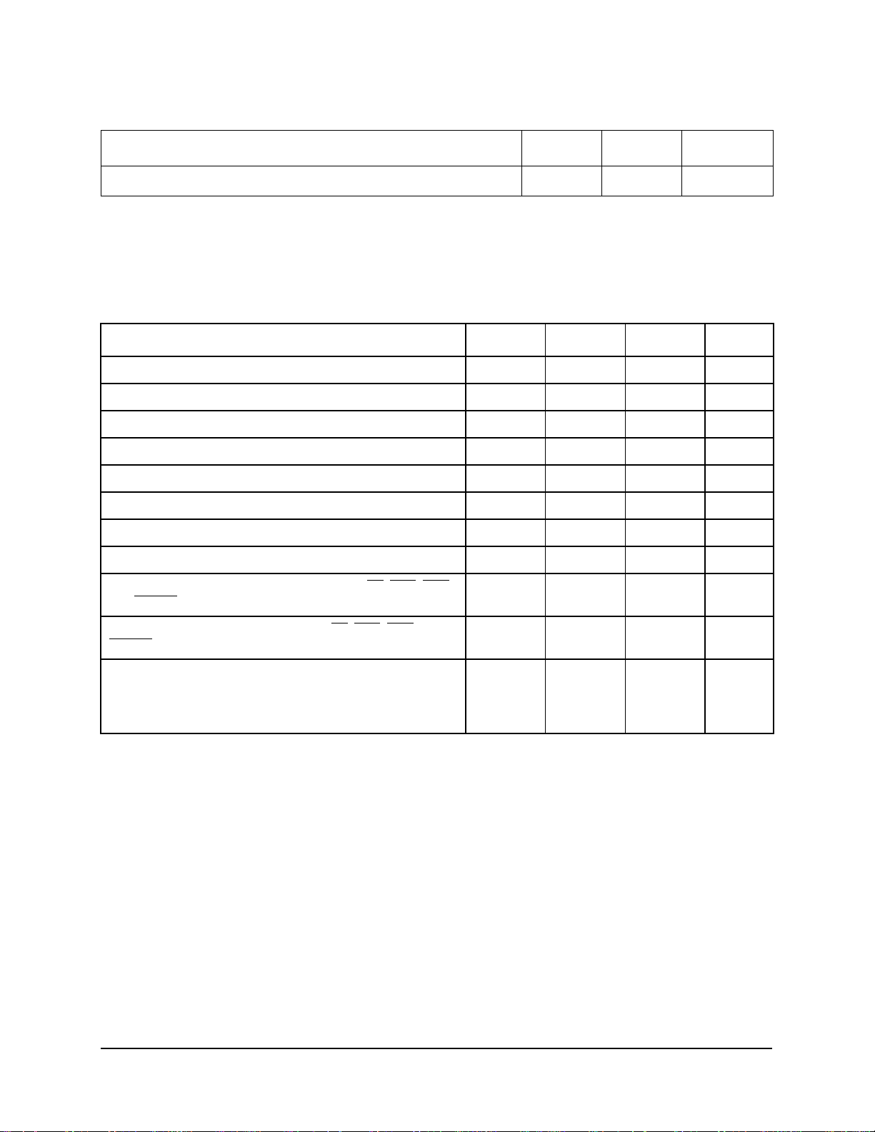
Table 3 provides the thermal characteristics for the 604e.
Table 3. Thermal Characteristics
Characteristic Symbol Value Rating
CBGA package thermal resistance, junction-to-top of die q
Note: Refer to Section 1.8, ÒSystem Design Information,Ó for more details about thermal management.
JC
0.03 ¡C/W
Table 4 provides the DC electrical characteristics for the 604e.
Table 4. DC Electrical Specifications
Vdd = AVdd = 1.9 ±100 mV dc, OVdd = 3.3 ± 5% V dc, GND = 0 V dc, 0 £ Tj £ 105 ¡C
Characteristic Symbol Min Max Unit
Input high voltage (all inputs except SYSCLK) V
Input low voltage (all inputs except SYSCLK) V
SYSCLK input high voltage CV
SYSCLK input low voltage CV
Input leakage current, Vin = 3.3 V
Hi-Z (off-state) leakage current, V
Output high voltage, I
Output low voltage, I
Capacitance, V
and AR
TRY)
Capacitance, V
AR
TRY)
Output impedance
Normal mode (DRV_MOD[0Ð1] = 01)
Strong mode (DRV_MOD[0Ð1] = 10)
Herculean mode (DRV_MOD[0Ð1] = 11)
in =
in =
= Ð2
OH
2
=
OL
0 V, f = 1 MHz
0 V, f = 1 MHz
1
3.3 V
1
=
in
mA V
mA V
2
(excludes TS, ABB, DBB,
2
(for TS, ABB, DBB, and
I
I
C
C
in
TSI
PRELIMINARY
Z
IH
IL
IH
IL
OH
OL
in
in
o
2.0 3.465 V
0.0 0.8 V
2.4 3.465 V
0.0 0.4 V
Ñ10µA
Ñ10µA
2.4 Ñ V
Ñ 0.4 V
Ñ 10.0 pF
Ñ 15.0 pF
56
42
30
84
57
30
W
Notes :
1. Excludes test signals (LSSD_MODE, L1_TSTCLK, L2_TSTCLK, and JTAG signals).
2. Capacitance values are guaranteed by design and characterization, and are not tested.
3. Output impedance is guaranteed by design and is not tested. Refer to IBIS simulation models for output
impedance values based on Vdd and OVdd tolerances used in system.
PID9q-604e Hardware Specifications 7
PRELIMINARYÑSUBJECT TO CHANGE WITHOUT NOTICE
Page 8

Table 5 provides the power consumption for the 604e.
£
£
Table 5. Power Consumption
CPU Clock:
SYSCLK
Full-On Mode
Typical
Maximum
Nap Mode
Typical
Maximum
Notes:
1. These values apply for all valid PLL_CFG[0Ð3] settings and do not include output
driver power (OVdd) or analog supply power (AVdd). OVdd power is system
dependent but is typically
2. Typical power is an average value estimated at Vdd = AVdd = 1.9 V, OVdd = 3.3 V, T
25 ¡C in a system executing typical applications and benchmark sequences. Typical
power numbers should be used in planning for proper thermal management.
3. Maximum power is estimated at Vdd = AVdd = 2.0 V, OVdd = 3.465 V,T
worst-case instruction mix. These values should be used for power supply design.
4. Nap mode power consumption is estimated, and assumes no snoop activity.
266 MHz 300 MHz 333 MHz
6.0 6.8 7.5 W
10.6 12.0 13.4 W
TBD TBD TBD W
0.78 0.80 0.82 W
Processor Core Frequency
10% of Vdd. Worst-case AVdd = 15 mW.
= 0 ¡C using a
j
Unit
=
j
1.4.2 AC Electrical Characteristics
This section provides the AC electrical characteristics for the 604e. These speciÞcations are for 266, 300,
and 333 MHz processor core frequencies. The processor core frequency is determined by the bus
(SYSCLK) frequency and the settings of the PLL_CFG[0Ð3] signals. All timings are speciÞed respective to
the rising edge of SYSCLK.
1.4.2.1 Clock AC SpeciÞcations
Table 6 provides the clock AC timing speciÞcations as deÞned in Figure 1.
Vdd = AVdd = 1.9 ±100 mV dc, OVdd = 3.3 ± 5% V dc, GND = 0 V dc, 0 £ T
Num Characteristic
Processor frequency 250 266 266 300 300 333 MHz 1
VCO frequency 500 532 532 600 600 666 MHz 1
SYSCLK frequency 35.7 100 38 100 42.9 100 MHz 1, 6
1 SYSCLK cycle time 10 35 10 28 10 25 ns
2, 3 SYSCLK rise and fall time 1.0 2.0 1.0 2.0 1.0 2.0 ns 2
PRELIMINARY
Table 6. Clock AC Timing Specifications
105 ¡C
j
266 MHz 300 MHz 333 MHz
Unit Notes
Min Max Min Max Min Max
8 PID9q-604e Hardware Specifications
PRELIMINARYÑSUBJECT TO CHANGE WITHOUT NOTICE
Page 9
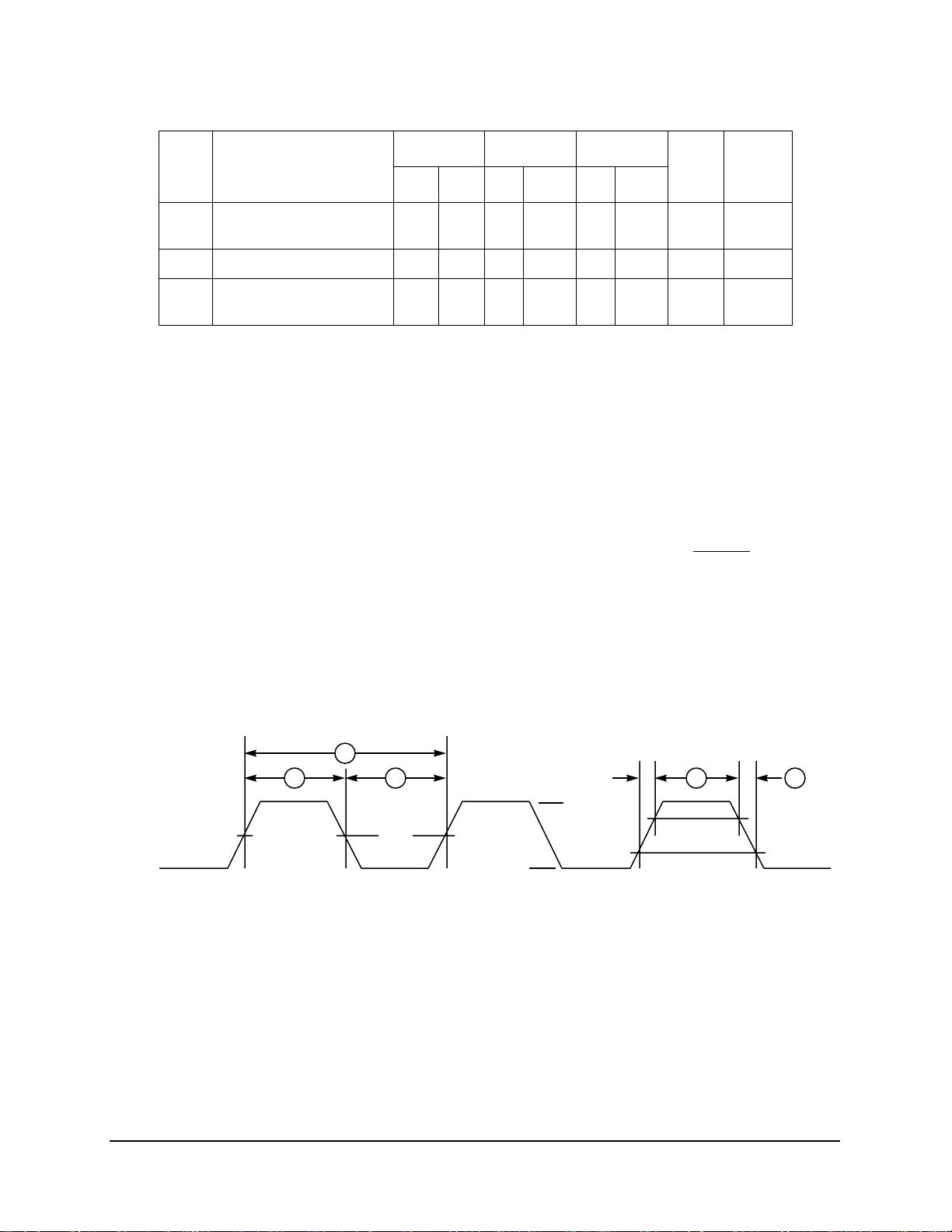
Table 6. Clock AC Timing Specifications (Continued)
Vdd = AVdd = 1.9 ±100 mV dc, OVdd = 3.3 ± 5% V dc, GND = 0 V dc, 0 £ Tj £ 105 ¡C
266 MHz 300 MHz 333 MHz
Num Characteristic
Min Max Min Max Min Max
Unit Notes
4 SYSCLK duty cycle
measured at 0.9 V
SYSCLK jitter Ñ ±150 Ñ ±150 Ñ ±150 ps 4
604e internal PLL relock
time
Notes:
1. Caution: The SYSCLK frequency and PLL_CFG[0Ð3] settings must be chosen such that the
resulting SYSCLK (bus) frequency, CPU (core) frequency, and PLL (VCO) frequency do not
exceed their respective maximum or minimum operating frequencies. Refer to the
PLL_CFG[0Ð3] signal description in Section 1.8, ÒSystem Design Information,Ó for valid
PLL_CFG[0Ð3] settings, and to Section 1.9, ÒOrdering Information,Ó for available frequencies
and part numbers.
2. Rise and fall times for the SYSCLK input are measured from 0.4 V to 1.8 V.
3. Timing is guaranteed by design and characterization, and is not tested.
4. Cycle-to-cycle jitter, and is guaranteed by design.
5. PLL-relock time is the maximum time required for PLL lock after a stable Vdd, OVdd, AVdd,
and SYSCLK are reached during the power-on reset sequence. Also note that HRESET
must be held asserted for a minimum of 255 bus clocks after the PLL-relock time (100 ms)
during the power-on reset sequence.
6. 604e processors are tested at the maximum SYSCLK frequencies shown in the AC timing
speciÞcations. It is possible to attain higher SYSCLK frequencies through proper system
design.
40 60 40 60 40 60 % 3
Ñ 100 Ñ 100 Ñ 100 ms 3, 5
Figure 1 provides the SYSCLK input timing diagram.
PRELIMINARY
1
4
SYSCLK
Figure 1. SYSCLK Input Timing Diagram
VM
VM = Midpoint Voltage (0.9 V)
2 34
CVih
CVil
PID9q-604e Hardware Specifications 9
PRELIMINARYÑSUBJECT TO CHANGE WITHOUT NOTICE
Page 10

1.4.2.2 Input AC SpeciÞcations
Table 7 provides the input AC timing speciÞcations for the 604e as deÞned in Figure 2. These speciÞcations
are for 266, 300, and 333 MHz processor core frequencies.
Table 7. Input AC Timing Specifications
Vdd = AVdd = 1.9 ±100 mV dc, OVdd = 3.3 ± 5% V dc, GND = 0 V dc, 0 £ Tj £ 105 ¡C
Num Characteristic
7a AR
7b All other inputs valid to SYSCLK (input setup)
8 SYSCLK to all inputs invalid (input hold) Ð0.5 Ñ ns
9 Mode select input valid to HRESET
10 HRESET
Notes:
TRY, SHD, ABB, TS, XATS, AACK,BG, DRTRY, TA, DBG,
DBB
, TEA, DBDIS, and DBWO valid to SYSCLK (input setup)
7
(input setup for DRTRY) 8 * t
to mode select input invalid (input hold for DRTRY) Ð0.5 Ñ ns 3, 4, 5,
1. Input speciÞcations are measured from the TTL level (0.8 or 2.0 V) of the signal in question to the 0.9 V of
the rising edge of the input SYSCLK. Input and output timings are measured at the pin (see Figure 2).
2. All other input signals include the following signalsÑall inputs except AR
BG
, DRTRY, TA, DBG, DBB, DBWO, DBDIS, TEA, and JTAG inputs.
3. The setup and hold time is with respect to the rising edge of HRESET
4. t
5. These values are guaranteed by design, and are not tested.
6. Note this is for conÞguration of the fast-L2 mode and the no-DR
7. Setup time is extended by 0.5 ns for these signals when Hysteresis On mode is enabled.
is the period of the external clock (SYSCLK) in nanoseconds.
sysclk
PRELIMINARY
TRY mode.
1
266, 300, 333 MHz
Unit Notes
Min Max
3.50 Ñ ns
2.50 Ñ ns 2
sysclk
TRY, SHD, ABB, TS, XATS, AACK,
(see Figure 3).
Ñ ns 3, 4, 5,
6
6
Figure 2 provides the input timing diagram for the 604e.
SYSCLK
7
ALL INPUTS
10 PID9q-604e Hardware Specifications
PRELIMINARYÑSUBJECT TO CHANGE WITHOUT NOTICE
VM
8
VM = Midpoint Voltage (0.9 V)
Figure 2. Input Timing Diagram
Page 11

Figure 3 provides the mode select input timing diagram for the 604e.
HRESET
9
DRTRY
VM = Midpoint Voltage (0.9 V)
VM
10
Figure 3. Mode Select Input Timing Diagram
1.4.2.3 Output AC SpeciÞcations
The output speciÞcations of the 604e for both driving high and driving low depend on the capacitive loading
on each output and the drive capability enabled for that output. Additionally, the timing speciÞcations for
outputs driving low also depend on the voltage swing required to drive to 0.4V. Table 8 provides the output
AC timing speciÞcations for a 5pF, 50 W
speciÞcations for a given set of conditions, it is recommended that IBIS simulation models be used. The
IBIS models are currently based on device simulation data. Compatibility mode speciÞcations are provided
to support PID9q-604e use in existing designs. Contact the local Motorola or IBM sales ofÞce for
information on the availability of these models.
transmission line load. In order to derive the actual timing
Table 8 provides the output AC timing speciÞcations for the 604e (refer to Figure 4).
Table 8. Output AC Timing Specifications1
Vdd = AVdd = 1.9 ±100 mV dc, OVdd = 3.3 ± 5% V dc, GND = 0 V dc, 0 £ Tj £ 105 ¡C, drive mode [11]
PRELIMINARY
Num Characteristic
Min Max
11 SYSCLK to output driven (output enable time) 0.75 Ñ 0.75 Min ns 2, 5
12 SYSCLK to TS
DBB
output valid
13 SYSCLK to all other signals output valid Ñ 4.75 5.75 Max ns 5
14 SYSCLK to output invalid (output hold) 0.0 0.5 Min ns 2, 5
15 SYSCLK to output high impedance (all signals
except AR
XA
TS)
16 SYSCLK to output high impedance
17 SYSCLK to ABB
after precharge
18 SYSCLK to AR
before precharge
, XATS, ARTRY, SHD, ABB and
TRY, SHD, ABB, DBB, TS, and
TS, XATS Ñ 3.4 4.4 Max ns 5
and DBB high impedance
TRY and SHD high impedance
Ñ 3.75 4.75 Max ns 5
Ñ 3.4 4.4 Max ns 5
Ñ 1.0* t
Ñ 3.4 4.4 Max ns 5
266, 300, 333 MHz
sysclk
6
Compatibility
Mode
1.0* t
sysclk
Max
Unit Notes
ns 4
PID9q-604e Hardware Specifications 11
PRELIMINARYÑSUBJECT TO CHANGE WITHOUT NOTICE
Page 12

Table 8. Output AC Timing Specifications1 (Continued)
Vdd = AVdd = 1.9 ±100 mV dc, OVdd = 3.3 ± 5% V dc, GND = 0 V dc, 0 £ Tj £ 105 ¡C, drive mode [11]
266, 300, 333 MHz
Num Characteristic
Min Max
Compatibility
6
Unit Notes
Mode
19 SYSCLK to ARTRY, and SHD precharge
enable
20 Maximum delay to AR
21 SYSCLK to AR
after precharge
Rise time (AR
XA
TS)
Rise time (all signals except AR
ABB
, DBB, TS, and XATS)
Fall time (AR
XA
TS)
Fall time (all signals except AR
DBB
, TS, and XATS)
Notes:
1. All output speciÞcations are measured from the 0.9 V level of the rising edge of SYSCLK to the TTL level (0.5
V or 2.0 V) of the signal in question. Both input and output timings are measured at the pin (see Figure 4).
2. All AC timing is based on a 5pF, 50
3. These speciÞcations are nominal values
4. t
5. These speciÞcations are nominal values for Fast Out mode; refer to Section 1.8.2, ÒInput and Output Signal
6. To operate in accordance with these speciÞcations, the drive mode signals must be conÞgured with
is the period of the external bus clock (SYSCLK) in nanoseconds (ns). When the unit is given as t
sysclk
the numbers given in the table must be multiplied by the period of SYSCLK to compute the actual time
duration (in nanoseconds) of the parameter in question.
Mode SelectionÓ for signal conÞguration to enable Fast Out mode.The PID9q-604e is tested in Fast Out mode.
Compatibility mode is guaranteed by design and is not tested.
DRVMOD0 = high, and DRVMOD1 = high.
TRY, SHD, ABB, DBB, TS, and
TRY, SHD, ABB, DBB, TS, and
TRY and SHD precharge
TRY and SHD high impedance
TRY, SHD,
TRY, SHD, ABB,
W transmission line load
PRELIMINARY
0.5* t
Ñ 1.5* t
Ñ 2.0* t
1.0 1.0 1.0 ns 3
1.0 1.0 1.0 ns 3
1.0 1.0 1.0 ns 3
1.0 1.0 1.0 ns 3
+ 0.75 Ñ 0.5* t
sysclk
sysclk
sysclk
1.5* t
2.0* t
sysclk
sysclk
sysclk
+ 0.75 Max
Max
Max
ns 4
ns 4
ns 4
sysclk
12 PID9q-604e Hardware Specifications
PRELIMINARYÑSUBJECT TO CHANGE WITHOUT NOTICE
Page 13

Figure 4 provides the output timing diagram for the 604e.
SYSCLK
ALL OUTPUTS
(Except TS, ABB,
ARTRY, XATS, SHD)
, XATS
TS
ABB, DBB
ARTRY, SHD
DBB
VM
13
11
,
12
VM
14
15
12
17
20
19
18
VM
14
16
21
VM = Midpoint Voltage (
0.9 V)
Figure 4. Output Timing Diagram
1.4.3 JTAG AC Timing SpeciÞcations
PRELIMINARY
Table 9 provides the JTAG AC timing speciÞcations.
Table 9. JTAG AC Timing Specifications (Independent of SYSCLK)
Vdd = AVdd = 1.9 ±100 mV dc, OVdd = 3.3 ± 5%, GND = 0 V dc, CL = 5 pF, 0 £ Tj £ 105 ¡C
Num Characteristic Min Max Unit Notes
TCK frequency of operation 0 16 MHz
1 TCK cycle time 62.5 Ñ ns
2 TCK clock pulse width measured at 0.9 V 25 Ñ ns
3 TCK rise and fall times 0 3 ns
4 TRST
5 TRST
6 Boundary-scan input data setup time 0 Ñ ns 2
setup time to TCK rising edge 13 Ñ ns 1
assert time 40 Ñ ns
7 Boundary-scan input data hold time 27 Ñ ns 2
PID9q-604e Hardware Specifications 13
PRELIMINARYÑSUBJECT TO CHANGE WITHOUT NOTICE
Page 14

Table 9. JTAG AC Timing Specifications (Independent of SYSCLK) (Continued)
Vdd = AVdd = 1.9 ±100 mV dc, OVdd = 3.3 ± 5%, GND = 0 V dc, CL = 5 pF, 0 £ Tj £ 105 ¡C
Num Characteristic Min Max Unit Notes
8 TCK to output data valid 4 25 ns 3
9 TCK to output high impedance 3 24 ns 3
10 TMS, TDI data setup time 0 Ñ ns
11 TMS, TDI data hold time 25 Ñ ns
12 TCK to TDO data valid 4 24 ns
13 TCK to TDO high impedance 3 15 ns
Notes:
1. TRST
2. Non-test signal input timing with respect to TCK.
3. Non-test signal output timing with respect to TCK.
is an asynchronous signal. The setup time is for test purposes only.
Figure 5 provides the JTAG clock input timing diagram.
TCK
3
VM = Midpoint Voltage (0.9 V)
PRELIMINARY
Figure 5. Clock Input Timing Diagram
Figure 6 provides the TRST timing diagram.
TCK
TRST
Figure 6. TRST Timing Diagram
1
2
VM
3
4
5
VM
2
VM
14 PID9q-604e Hardware Specifications
PRELIMINARYÑSUBJECT TO CHANGE WITHOUT NOTICE
Page 15

Figure 7 provides the boundary-scan timing diagram.
TCK
6 7
Data Inputs
8
Data Outputs
9
Data Outputs
8
Data Outputs
Figure 7. Boundary-Scan Timing Diagram
Figure 8 provides the test access port timing diagram.
TCK
TDI, TMS
Input Data Valid
Output Data Valid
Output Data Valid
10 11
Input Data Valid
TDO
TDO
TDO
12
PRELIMINARY
Output Data Valid
13
12
Output Data Valid
Figure 8. Test Access Port Timing Diagram
PID9q-604e Hardware Specifications 15
PRELIMINARYÑSUBJECT TO CHANGE WITHOUT NOTICE
Page 16

1.5 Pin Assignments
Motorola and IBM both offer a ceramic ball grid array (CBGA) package. Both IBM and Motorola CBGA
packages have identical pinouts. Figure 9 (in part A) shows the pinout of the CBGA package as viewed from
the top surface. Part B shows the side proÞle of the CBGA package to indicate the direction of the top
surface view.
Part A
01 02 03 04 05 06 07 08 09 10 11 12 13 14 15 16
A
B
C
D
E
F
G
H
J
K
Part B
L
M
N
P
R
T
PRELIMINARY
Not to Scale
Substrate Assembly
Encapsulant
Figure 9. Pinout of the CBGA Package as Viewed from the Top Surface
View
Die
16 PID9q-604e Hardware Specifications
PRELIMINARYÑSUBJECT TO CHANGE WITHOUT NOTICE
Page 17

1.6 Pinout Listings
Table 10 provides the pinout listing for the 604e CBGA package.
Table 10. Pinout Listing for the CBGA Package
Signal Name Pin Number Active I/O
A[0Ð31] C16, E04, D13, F02, D14, G01, D15, E02, D16, D04, E13,
GO2, E15, H01, E16, H02, F13, J01, F14, J02, F15, H03,
F16, F04, G13, K01, G15, K02, H16, M01, J15, P01
CK L02 Low Input
AA
ABB
AP[0Ð3] C01, B04, B03, B02 High I/O
APE
ARRAY_WR
AR
TRY J04 Low I/O
AVDD A10 Ñ Ñ
BG
BR
CI
CKSTP_IN
CKSTP_OUT
CLK_OUT D07 Ñ Output
CSE[0Ð1] B01, B05 High Output
1
K04 Low I/O
A04 Low Output
B07 Low Input
L01 Low Input
B06 Low Output
E01 Low Output
D08 Low Input
A06 Low Output
High I/O
DBB
DBG
DBDIS
DBW
O G04 Low Input
DH[0Ð31] P14, T16, R15, T15, R13, R12, P11, N11, R11,T12, T11,
DL[0Ð31] K13, K15, K16, L16, L15, L13, L14, M16, M15, M13, N16,
DP[0Ð7] M02, L03, N02, L04, R01, P02, M04, R02 High I/O
DPE
DR
TRY G16 Low Input
DRVMOD0
DRVMOD1
GBL
3
3
J14 Low I/O
PRELIMINARY
N01 Low Input
H15 Low Input
High I/O
R10, P09, N09, T10, R09, T09, P08, N08, R08, T08, N07,
R07, T07, P06, N06, R06, T06, R05, N05, T05, T04
High I/O
N15, N13, N14, P16, P15, R16, R14, T14, N10, P13, N12,
T13, P03, N03, N04, R03, T01, T02, P04, T03, R04
A05 Low Output
D05 High Input
C03 High Input
F01 Low I/O
PID9q-604e Hardware Specifications 17
PRELIMINARYÑSUBJECT TO CHANGE WITHOUT NOTICE
Page 18

Table 10. Pinout Listing for the CBGA Package (Continued)
Signal Name Pin Number Active I/O
GND C05, C12, E03, E06, E08, E09, E11, E14, F05, F07, F10,
F12, G06, G08, G09, G11, H05, H07, H10, H12, J05, J07,
J10, J12, K06, K08, K09, K11, L05, L07, L10, L12, M03,
M06, M08, M09, M11, M14, P05, P12
HALTED B08 High Output
HRESET
INT
L1_TSTCLK
L2_INT D06 High Input
L2_TSTCLK
LSSD_MODE
MCP
OVDD C07, E05, E07, E10, E12, G03, G05, G12, G14, K03, K05,
PLL_CFG[0Ð3] A08, B09, A09, D09 High Input
RSR
V D01 Low Output
RUN C08 High Input
1
1
1
A07 Low Input
B15 Low Input
D11 Low Input
D12 Low Input
B10 Low Input
C13 Low Input
K12, K14, M05, M07, M10, M12, P07, P10
ÑÑ
ÑÑ
SHD
SMI
SRESET
SYSCLK C09 Ñ Input
T
A H14 Low Input
TBEN C02 High Input
TBST
TC[0Ð2] A02, A03, C06 High Output
TCK C11 High Input
TDI A11 High Input
TDO A12 High Output
TEA
TMS B11 High Input
TRST
TS
TSIZ[0Ð2] A13, D10, B12 High I/O
H04 Low I/O
A16 Low Input
B14 Low Input
PRELIMINARY
A14 Low I/O
H13 Low Input
C10 Low Input
J13 Low I/O
TT[0Ð4] B13, A15, B16, C14, C15 High I/O
18 PID9q-604e Hardware Specifications
PRELIMINARYÑSUBJECT TO CHANGE WITHOUT NOTICE
Page 19

Table 10. Pinout Listing for the CBGA Package (Continued)
Signal Name Pin Number Active I/O
WT D02 Low Output
VDD F06, F08, F09, F11, G07, G10, H06, H08, H09, H11, J06,
J08, J09, J11, K07, K10, L06, L08, L09, L11
VOLTDETGND
XA
TS J16 Low I/O
Notes:
1. These are test signals for factory use only and must be pulled up to Vdd for normal machine operation.
2. NC (no-connect) in the 604; internally tied to GND in the 604e CBGA package to indicate to the power
3. To operate in accordance with these speciÞcations, the drive mode signals must be conÞgured with
2
supply that a low-voltage processor is present.
DRVMOD0 = high, and DRVMOD1 = high.
F03
ÑÑ
1.7 Package Description
The package parameters for the 604e are provided in the following list. The package type is 21 mm, 256lead ceramic ball grid array (CBGA).
Package outline 21 x 21 mm
Interconnects 255
Pitch 1.27 mm (50 mil)
Maximum module height 3.30 mm
Ball diameter 0.89 mm (35 mil)
PRELIMINARY
PID9q-604e Hardware Specifications 19
PRELIMINARYÑSUBJECT TO CHANGE WITHOUT NOTICE
Page 20

1.7.0.1 Mechanical Dimensions of the CBGA Package
E
G
Figure 10 provides the mechanical dimensions and bottom surface nomenclature of the IBM and Motorola
CBGA package.
2X
0.2
A1 CORNER
D
A
C
0.15 C
E
2X
0.2
B
12345678910111213141516
e/2
D1
PRELIMINARY
e
e/2
T
R
P
N
M
L
K
J
H
G
F
E
D
C
B
A
E1
NOTES:
1. DIMENSIONING AND TOLERANCING PER ASME
Y14.5M, 1994.
2. DIMENSIONS IN MILLIMETERS.
3. TOP SIDE A1 CORNER INDEX IS A METALIZED
FEATURE WITH VARIOUS SHAPES. BOTTOM SID
A1 CORNER IS DESIGNATED WITH A BALL MISSIN
FROM THE ARRAY.
Millimeters
DIM MIN MAX
A 2.50 3.30
A1 0.79 0.99
A2 1.00 1.40
A2
A1
A
b 0.82 0.93
D 21.00 BSC
D1 5.00 16.00
e 1.27 BSC
E 21.00 BSC
E1 5.00 16.00
255X
b
BC
A0.3
C
0.15
Figure 10. Mechanical Dimensions and Bottom Surface Nomenclature of the CBGA Package
1.8 System Design Information
This section provides electrical and thermal design recommendations for successful application of the 604e.
1.8.1 PLL ConÞguration
The 604e PLL is conÞgured by the PLL_CFG[0Ð3] signals. For a given SYSCLK (bus) frequency, the PLL
conÞguration signals set the internal CPU and VCO frequency of operation. The PLL conÞguration for the
604e is shown in Table 11 for nominal frequencies.
20 PID9q-604e Hardware Specifications
PRELIMINARYÑSUBJECT TO CHANGE WITHOUT NOTICE
Page 21

Table 11. PLL Configuration
PLL_CFG
[0Ð3]
Bin Dec
0000 0 1:1 x2 Ñ Ñ Ñ Ñ Ñ Ñ Ñ Ñ
0001 1 1:1 x8 Ñ Ñ 40
1100 12 1.5:1 x2 Ñ Ñ Ñ Ñ Ñ Ñ Ñ Ñ
0100 4 2:1 x2 Ñ Ñ Ñ Ñ Ñ Ñ Ñ 200
0110 6 2.5:1 x2 Ñ Ñ Ñ Ñ Ñ Ñ 208
1000 8 3:1 x2 Ñ Ñ Ñ Ñ Ñ 200
1110 14 3.5:1 x2 Ñ Ñ Ñ Ñ 210
1010 10 4:1 x2 Ñ Ñ Ñ 200
CPU/
SYSCLK
Ratio
VCO
Multiplier
Bus
25
MHz
Bus
33.3
MHz
CPU Frequency in MHz
(VCO Frequency in MHz)
Bus
MHz
(320)50(400)60(480)66(533)
40
Bus
50
MHz
(400)
Bus
60
MHz
(420)
240
(480)
Bus
66.6
MHz
(400)
233
(466)
266
(532)
Bus
83.3
MHz
83.3
(666)
(416)
250
(500)
292
(584)
333
(666)
Bus
100
MHz
Ñ
(400)
250
(500)
300
(600)
350
(700)
Ñ
0111 7 4.5:1 x2 Ñ Ñ Ñ 225
(450)
1011 11 5:1 x2 Ñ Ñ 200
(400)
1001 9 5.5:1 x2 Ñ Ñ 220
PRELIMINARY
1101 13 6:1 x2 Ñ 200
(400)
0101 5 6.5:1 x2 Ñ 216
(433)
0010 2 7:1 x2 Ñ 233
(466)
0011 3 PLL bypass
1111 15 Clock off
Notes:
1. Some PLL conÞgurations may select bus, CPU, or VCO frequencies which are not supported; see
Section 1.4.2.2, ÒInput AC SpeciÞcations,Ó for valid SYSCLK and VCO frequencies.
2. In PLL-bypass mode, the SYSCLK input signal clocks the internal processor directly, the PLL is
disabled, and the bus mode is set for 1:1 mode operation. This mode is intended for factory use only.
Note: The AC timing speciÞcations given in this document do not apply in PLL-bypass mode.
(440)
240
(480)
260
(520)
280
(560)
250
(500)
275
(550)
300
(600)
325
(650)
350
(700)
270
(540)
300
(600)
330
(660)
ÑÑÑÑ
ÑÑÑÑ
ÑÑÑÑ
300
(600)
333
(666)
ÑÑÑ
ÑÑ
ÑÑ
PID9q-604e Hardware Specifications 21
PRELIMINARYÑSUBJECT TO CHANGE WITHOUT NOTICE
Page 22

1.8.2 Input and Output Signal Mode Selection
The PID9q-604eÕs input buffers can be conÞgured through the connection of the ARRAY_WR signal to
provide input hysteresis and enable the CLKOUT signal. If the ARRAY_WR signal is connected to OVdd,
the PID9q-604e will select the Hysteresis Off input buffer threshold mode, and the CLKOUT signal is
enabled, which is the default mode for this speciÞcation. When Hysteresis OFF mode is selected the VM is
0.9V.
If ARRAY_WR is connected to GND, Hysteresis On mode is selected, and the CLKOUT signal is placed
in a high impedance state. When Hysteresis On mode is selected, the VM is 1.3V, and the input transition
points are 1.1V for V
inputs, and the input hold time requirement for Low to High transitions is increased.
and 1.5V for VIH. Hysteresis On mode provides for greater noise immunity on
IL
When the ARRAY_WR signal is connected to the HRESET
CLKOUT signal is enabled. If the ARRAY_WR signal is connected to an inverted HRESET
Hysteresis Off mode is selected, and the CLKOUT signal is placed in a high impedance state.
Table 12 below shows the conÞguration of the ARRAY_WR signal to select input signal hysteresis and
enable the CLKOUT signal.
Table 12. Input Signal Hysteresis and CLKOUT Signal Configuration
Signal Connected to Mode Selected Notes
ARRAY_WR OVdd Hyteresis Off
GND Hyteresis On
HRESET
HRESET Hyteresis Off
signal Hyteresis On
signal, Hysteresis On mode is selected, and the
signal,
1
CLKOUT Enabled
CLKOUT high impedance
CLKOUT Enabled
2
CLKOUT high impedance
PRELIMINARY
Notes:
1. Default Mode
2.HRESET is the inverted state of the HRESET
signal
The PID9q-604e implements a Fast Out output mode which allows increased system bus frequencies. The
PID9q-604e can be conÞgured for Fast Out mode by connecting the L2_TSTCLK signal to GND or the
HRESET
L2_TSTCLK signal is connected to OVdd or to an inverted HRESET
22 PID9q-604e Hardware Specifications
signal. When Fast Out mode is enabled, the output valid and output hold times are reduced. If the
, compatibility mode is selected.
PRELIMINARYÑSUBJECT TO CHANGE WITHOUT NOTICE
Page 23

Table 13 describes the conÞguration of the L2_TSTCLK signal to select Fast Out or compatibility output
modes.
Table 13. FastOut/Compatibility Output Signal Configuration
Signal Connected to Mode Selected Notes
L2_TSTCLK OVdd Compatibility
GND FastOut 1
HRESET
HRESET Compatibility 2
Notes:
1. Default Mode
2.HRESET is the inverse state of the HRESET
signal
FastOut
1.8.3 PLL Power Supply Filtering
The AVdd power signal is provided on the 604e to provide power to the clock generation phase-locked loop.
To ensure stability of the internal clock, the power supplied to the AVdd input signal should be Þltered using
a circuit similar to the one shown in Figure 11. The circuit should be placed as close as possible to the AVdd
pin to ensure it Þlters out as much noise as possible.
W
10
Vdd AVdd
(1.8 V Nom.)
Figure 11. PLL Power Supply Filter Circuit
PRELIMINARY
10 µF 0.1 µF
GND
1.8.4 Decoupling Recommendations
Due to the 604eÕs large address and data buses, and high operating frequencies, the 604e can generate
transient power surges and high frequency noise in its power supply, especially while driving large
capacitive loads. This noise must be prevented from reaching other components in the 604e system, and the
604e itself requires a clean, tightly regulated source of power. Therefore, it is strongly recommended that
the system designer place at least one decoupling capacitor with a low ESR (effective series resistance)
rating at each Vdd and OVdd pin of the 604e.
These capacitors should range in value from 220 pF to 10 mF to provide both high- and low-frequency
Þltering, and should be placed as close as possible to their associated Vdd pin. Surface-mount tantalum or
ceramic devices are preferred. It is also recommended that these decoupling capacitors receive their power
from Vdd and GND power planes in the PCB, utilizing short traces to minimize inductance in the traces.
Power and ground connections must be made to all external Vdd and GND pins of the 604e.
1.8.5 Connection Recommendations
To ensure reliable operation, it is recommended to connect unused inputs to an appropriate signal level.
Unused active low inputs should be tied to Vdd. Unused active high inputs should be connected to GND.
PID9q-604e Hardware Specifications 23
PRELIMINARYÑSUBJECT TO CHANGE WITHOUT NOTICE
Page 24

1.8.6 Thermal Management Information
This section provides thermal management information for the ceramic ball grid array (CBGA) package for
air-cooled applications. Proper thermal control design is primarily dependent upon the system-level
designÑthe heat sink, airßow and thermal interface material. To reduce the die-junction temperature, heat
sinks may be attached to the package by several methodsÑadhesive, spring clip to holes in the printedcircuit board or package, and mounting clip and screw assembly; see Figure 12. This spring force should
not exceed 5.5 pounds of force.
Heat Sink
Heat Sink
Clip
Adhesive
Thermal Interface Material
Figure 12. Package Exploded Cross-Sectional View with Several Heat Sink Options
The board designer can choose between several types of heat sinks to place on the 604e. There are several
commercially-available heat sinks for the 604e provided by the following vendors:
Thermalloy
2021 W. Valley View Lane 214-243-4321
P.O. Box 810839
Dallas, TX 75731
PRELIMINARY
or
CBGA Package
Printed-Circuit Board
Option
International Electronic Research Corporation (IERC)
135 W. Magnolia Blvd.
Burbank, CA 91502 818-842-7277
Aavid Engineering 603-528-3400
One Kool Path
Laconic, NH 03247-0440
WakeÞeld Engineering 617-245-5900
60 Audubon Rd.
WakeÞeld, MA 01880
Ultimately, the Þnal selection of an appropriate heat sink for the 604e depends on many factors, such as
thermal performance at a given air velocity, spatial volume, mass, attachment method, assembly, and cost.
24 PID9q-604e Hardware Specifications
PRELIMINARYÑSUBJECT TO CHANGE WITHOUT NOTICE
Page 25

1.8.6.1 Internal Package Conduction Resistance
For the exposed-die packaging technology, shown in Table 14, the intrinsic conduction thermal resistance
paths are as follows:
¥ The die junction-to-case thermal resistance
¥ The die junction-to-lead thermal resistance
Table 14. Package Thermal Resistance
Thermal Metric CBGA
Junction-to-top of die thermal resistance 0.03 ¡C/W
Junction-to-lead (ball) thermal resistance 2.2 ¡C/W
Figure 13 depicts the primary heat transfer path for a package with an attached heat sink mounted to a
printed-circuit board.
External Resistance
Heat Sink
Internal Resistance
Printed-Circuit Board
External Resistance
Figure 13. C4 Package with Heat Sink Mounted to a Printed-Circuit Board
Heat generated on the active side (ball) of the chip is conducted through the silicon, then through the heat
sink attach material (or thermal interface material), and Þnally to the heat sink where it is removed by
forced-air convection.
PRELIMINARY
(Note the internal versus external package resistance)
Radiation Convection
Thermal Interface Material
Die/Package
Die Junction
Package/Leads
Radiation Convection
Since the silicon thermal resistance is quite small, for a Þrst-order analysis, the temperature drop in the
silicon may be neglected. Thus, the heat sink attach material and the heat sink conduction/convective
thermal resistances are the dominant terms. The following section provides a thermal management example
for the 604e using one of the commercially available heat sinks.
PID9q-604e Hardware Specifications 25
PRELIMINARYÑSUBJECT TO CHANGE WITHOUT NOTICE
Page 26

1.8.6.2 Thermal Management Example
For preliminary heat sink sizing, the die-junction temperature can be expressed as follows:
T
Where:
= Ta + Tr + (R
j
is the die-junction temperature
T
j
is the inlet cabinet ambient temperature
T
a
is the air temperature rise within the system cabinet
T
r
is the die-junction-to-top of die thermal resistance of the device
R
jc
q
is the thermal resistance of the thermal interface material (thermal grease or thermal compound)
R
a
is the heat sink-to-ambient thermal resistance
R
sa
q
Q is the power consumed by the device
jc +Ra
+ Rsa) * Q
Typical die-junction temperatures (T
) should be maintained less than 105 ¡C. The temperature of the air
j
cooling the component greatly depends upon the ambient inlet air temperature and the air temperature rise
within the computer cabinet. A computer cabinet inlet-air temperature (T
air temperature rise within a cabinet (T
interface material (R
) is typically about 1 ¡C/W. Assuming a Ta of 30 ¡C, a T
a
consumption (Q) of 7.5 watts, the following expression for T
Junction temperature: T
= 30 ¡C + 5 ¡C + (0.03 ¡C/W + 1.0 ¡C/W + Rsa) * 7.5 W
j
) may be in the range of 5 to 10 ¡C. The thermal resistance of the
r
is obtained:
j
For a Thermalloy heat sink #2333B, the heat sink-to-ambient thermal resistance (R
) may range from 30 to 40 ¡C. The
a
of 5 ¡C, and a power
r
) versus airßow
sa
velocity is shown in Figure 14.
8
7
6
5
PRELIMINARY
Thermalloy #2328B Pin-fin Heat Sink
(25 x28 x 15 mm)
4
3
Heat Sink Thermal Resistance (¼C/W)
2
1
0 0.5 1 1.5 2 2.5 3 3.5
Approach Air Velocity (m/s)
Figure 14. Thermalloy #2328B Heat Sink-to-Ambient Thermal Resistance Versus Airflow Velocity
26 PID9q-604e Hardware Specifications
PRELIMINARYÑSUBJECT TO CHANGE WITHOUT NOTICE
Page 27

Assuming an air velocity of 0.5 m/s, we have an effective Rsa of 5 ¡C/W, thus
T
= 30 ¡C + 5 ¡C + (0.03 ¡C/W + 1.0 ¡C/W + 5 ¡C/W) * 7.5 W,
j
resulting in a junction temperature of approximately 81 ¡C which is just below the maximum operating
temperature of the part. To ensure maximum reliability, it is desirable to operate the 604e well within its
operating temperature range. Thus, to keep a 7.5 W 604e within its proper operating range, an air velocity
greater than 0.5 m/s should be used with the Thermalloy #2333B pin-Þn heat sink.
Other heat sinks offered by Thermalloy, Aavid, WakeÞeld, and IERC offer different heat sink-to-ambient
thermal resistances, and may or may not need air ßow. It is necessary to perform an analysis as done above
to select the desired heat sink.
Though the junction-to-ambient and the heat sink-to-ambient thermal resistances are commonly used to
compare the thermal performance of various microelectronic packaging technologies, one should exercise
caution when only using this metric in determining thermal management because no single parameter can
adequately describe three-dimensional heat ßow. The Þnal chip-junction operating temperature is not only
a function of the component-level thermal resistance, but the system-level design and its operating
conditions. In addition to the component's power consumption, a number of factors affect the Þnal operating
die-junction temperature. These factors might include airßow, board population (local heat ßux of adjacent
components), heat sink efÞciency, heat sink attach, next-level interconnect technology, system air
temperature rise, etc. Due to the complexity and the many variations of system-level boundary conditions
for today's microelectronic equipment, the combined effects of the heat transfer mechanisms (radiation,
convection and conduction) may vary widely. For these reasons, we recommend using conjugate heat
transfer models for the board as well as system-level designs. To expedite system-level thermal analysis,
several ÒcompactÓ thermal-package models are available within FLOTHERM¨. These are available upon
request.
1.9 Ordering Information
This section provides the part numbering nomenclature for the 604e. Note that the individual part numbers
correspond to a speciÞc combination of 604e internal/bus frequencies, which must be observed to ensure
proper operation of the device. For available frequency combinations, contact your local Motorola or IBM
sales ofÞce.
In addition to the processor frequency and bus ratio, the part numbering scheme also consists of a part
modiÞer. The part modiÞer indicates the enhancement in the part from the original production design. Each
part number also contains a revision code. This refers to the die mask revision number and is speciÞed in
the part numbering scheme for identiÞcation purposes only.
PRELIMINARY
PID9q-604e Hardware Specifications 27
PRELIMINARYÑSUBJECT TO CHANGE WITHOUT NOTICE
Page 28

1.9.1 Motorola Part Number Key
Figure 15 provides the Motorola part numbering nomenclature for the 604e.
MPC 604 _ XX XXX X X
(Contact Local Motorola Sales Office)
Product Code
Part Identifier
Part Modifier
( = Enhanced and Lower Voltage Ñ604e)
Figure 15. Motorola Part Number Key
(Contact Local Motorola Sales Office
for Available Bus Ratios)
Processor Frequency
1.9.2 IBM Part Number Information
Contact your local IBM sales ofÞce for 604e part number and availability information.
Revision Level
Bus Divider
Package
(RX = BGA)
PRELIMINARY
28 PID9q-604e Hardware Specifications
PRELIMINARYÑSUBJECT TO CHANGE WITHOUT NOTICE
Page 29

Information in this document is provided solely to enable system and software implementers to use PowerPC microprocessors. There are no express or
implied copyright or patent licenses granted hereunder by Motorola or IBM to design, modify the design of, or fabricate circuits based on the information in
this document.
The PowerPC 604e microprocessor embodies the intellectual property of Motorola and of IBM. However, neither Motorola nor IBM assumes any responsibility
or liability as to any aspects of the performance, operation, or other attributes of the microprocessor as marketed by the other party or by any third party. Neither
Motorola nor IBM is to be considered an agent or representative of the other party or any third party, and neither has assumed, created, or granted hereby any
right or authority to the other, or to any third party, to assume or create any express or implied obligations on its behalf. Information such as errata sheets and
data sheets, as well as sales terms and conditions such as prices, schedules, and support, for the product may vary as between parties selling the product.
Accordingly, customers wishing to learn more information about the products as marketed by a given party should contact that party.
Both Motorola and IBM reserve the right to modify this document and/or any of the products as described herein without further notice. NOTHING IN THIS
DOCUMENT, NOR IN ANY OF THE ERRATA SHEETS, DATA SHEETS, AND OTHER SUPPORTING DOCUMENTATION, SHALL BE INTERPRETED AS THE
CONVEYANCE BY MOTOROLA OR IBM OF AN EXPRESS WARRANTY OF ANY KIND OR IMPLIED WARRANTY, REPRESENTATION, OR GUARANTEE
REGARDING THE MERCHANTABILITY OR FITNESS OF THE PRODUCTS FOR ANY PARTICULAR PURPOSE. Neither Motorola nor IBM assumes any
liability or obligation for damages of any kind arising out of the application or use of these materials. Any warranty or other obligations as to the products described
herein shall be undertaken solely by the marketing party to the customer, under a separate sale agreement between the marketing party and the customer. In the
absence of such an agreement, no liability is assumed by Motorola, IBM, or the marketing party for any damages, actual or otherwise.
ÒTypicalÓ parameters can and do vary in different applications. All operating parameters, including ÒTypicals,Ó must be validated for each customer application by
customerÕs technical experts. Neither Motorola nor IBM convey any license under their respective intellectual property rights nor the rights of others. Neither
Motorola nor IBM makes any claim, warranty, or representation, express or implied, that the products described in this document are designed, intended, or
authorized for use as components in systems intended for surgical implant into the body, or other applications intended to suppor t or sustain life, or for any other
application in which the failure of the product could create a situation where personal injury or death may occur. Should customer purchase or use the products
for any such unintended or unauthorized application, customer shall indemnify and hold Motorola and IBM and their respective ofÞcers, employees, subsidiaries,
afÞliates, and distributors harmless against all claims, costs, damages, and expenses, and reasonable attorneyÕs fees arising out of, directly or indirectly, any claim
of personal injury or death associated with such unintended or unauthorized use, even if such claim alleges that Motorola or IBM was negligent regarding the
design or manufacture of the part.
Motorola and are registered trademarks and Mfax is a trademark of Motorola, Inc. Motorola, Inc. is an Equal Opportunity/AfÞrmative Action Employer.
IBM, the IBM logo, and IBM Microelectronics are trademarks of International Business Machines Corporation.
The PowerPC name is a registered trademark and the PowerPC logotype, PowerPC 604 and PowerPC 604e are trademarks of International Business Machines
Corporation, used by Motorola under license from International Business Machines Corporation. International Business Machines Corporation is an Equal
Opportunity/AfÞrmative Action Employer.
International Business Machines Corporation:
IBM Microelectronics Division, 1580 Route 52, Bldg. 504, Hopewell
Junction, NY 12533-6531; Tel. (800) PowerPC
World Wide Web Address: http://www.chips.ibm.com/products/ppc
http://www.ibm.com
Motorola Literature Distribution Centers:
USA/EUROPE: Motorola Literature Distribution; P.O. Box 5405; Denver, Colorado 80217;
Tel.: 1-800-441-2447 or (303) 675-2140
JAPAN: Nippon Motorola Ltd.; Tatsumi-SPD-JLDC, 6F Seibu-Butsuryu-Center, 3-14-2
Tatsumi Koto-Ku, Tokyo 135, Japan; Tel.: 81-3-3521-8315
ASIA/PACIFC: Motorola Semiconductors H.K. Ltd.; 8B Tai Ping Industrial Park, 51 Ting
Kok Road, Tai Po, N.T., Hong Kong; Tel.: 852-26629298
Technical Information: Motorola Inc. SPS Customer Support Center; (800) 521-6274;
electronic mail address: crc@wmkmail.sps.mot.com.
Document Comments: FAX (512) 891-2638, Attn: RISC Applications Engineering.
 Loading...