

Page 1

查询MPC603E供应商
SA14-2027-00
(IBM Order Number)
(Motorola Order Number)
MPC603E/D
1/96
REV 1
Advance Information
PowerPC 603e
RISC Microprocessor
Technical Summary
This document provides an overview of the PowerPC 603e microprocessor features,
including a block diagram showing the major functional components. It also provides an
overview of the PowerPC
implementation complies with the architectural definitions.
This document is divided into two parts:
• Part 1, “PowerPC 603e Microprocessor Overview,” provides an overview of the
603e features, including a block diagram showing the major functional
components.
• Part 2, “PowerPC 603e Microprocessor: Implementation,” describes the PowerPC
architecture in general, as well as providing specific details about the
implementation of the 603e as a low-power, 32-bit member of the PowerPC
processor family , and an enumeration of the dif ferences from the PowerPC 603
microprocessor.
In this document, the term “603e” is used as an abbreviation for the phrase, “PowerPC 603e
microprocessor,” and the term “603” is used as an abbreviation for the phrase “PowerPC
603 microprocessor.” The PowerPC 603e microprocessors are available from IBM as
PPC603e and from Motorola as MPC603e.
architecture specification, and information about how the 603e
The PowerPC name, the PowerPC logotype, PowerPC 601, PowerPC 603, and PowerPC 603e are trademarks
Business Machines Corporation, used by Motorola under license from International Business Machines Corporation.
This document contains information on a new product under development by Motorola and IBM. Motorola and IBM reserve the right to
change or discontinue this product without notice.
Motorola Inc., 1996. All rights reserved
Portions hereof
International Business Machines Corporation, 1991–1996. All rights reserved
of International
603e Technical Summary
Page 2

2
Part 1 PowerPC 603e Microprocessor Overview
This section describes the features of the 603e, provides a block diagram showing the major functional units,
and gives an overview of how the 603e operates.
The 603e is a low-power implementation of the PowerPC microprocessor family of reduced instruction set
computer (RISC) microprocessors. The 603e implements the 32-bit portion of the PowerPC architecture,
which provides 32-bit effective addresses, integer data types of 8, 16, and 32 bits, and floating-point data
types of 32 and 64 bits.
The 603e provides four software controllable power-saving modes. Three of the modes (the nap, doze, and
sleep modes) are static in nature, and progressively reduce the amount of power dissipated by the processor.
The fourth is a dynamic power management mode that causes the functional units in the 603e to
automatically enter a low-power mode when the functional units are idle without affecting operational
performance, software execution, or any external hardware.
The 603e is a superscalar processor that can issue and retire as many as three instructions per clock.
Instructions can execute out of order for increased performance; however, the 603e makes completion
appear sequential.
The 603e integrates five execution units—an integer unit (IU), a floating-point unit (FPU), a branch
processing unit (BPU), a load/store unit (LSU), and a system register unit (SRU). The ability to execute five
instructions in parallel and the use of simple instructions with rapid execution times yield high efficiency
and throughput for 603e-based systems. Most integer instructions execute in one clock cycle. The FPU is
pipelined so a single-precision multiply-add instruction can be issued and completed every clock cycle.
The 603e provides independent on-chip, 16-Kbyte, four-way set-associative, physically addressed caches
for instructions and data and on-chip instruction and data memory management units (MMUs). The MMUs
contain 64-entry, two-way set-associative, data and instruction translation lookaside buffers (DTLB and
ITLB) that provide support for demand-paged virtual memory address translation and variable-sized block
translation. The TLBs and caches use a least recently used (LRU) replacement algorithm. The 603e also
supports block address translation through the use of two independent instruction and data block address
translation (IBAT and DBAT) arrays of four entries each. Effective addresses are compared simultaneously
with all four entries in the BA T array during block translation. In accordance with the PowerPC architecture,
if an effective address hits in both the TLB and BAT array, the BAT translation takes priority.
The 603e has a selectable 32- or 64-bit data bus and a 32-bit address bus. The 603e interface protocol allows
multiple masters to compete for system resources through a central external arbiter. The 603e provides a
three-state coherency protocol that supports the exclusive, modified, and invalid cache states. This protocol
is a compatible subset of the MESI (modified/exclusive/shared/invalid) four-state protocol and operates
coherently in systems that contain four-state caches. The 603e supports single-beat and burst data transfers
for memory accesses, and supports memory-mapped I/O operations.
The 603e is fabricated using an advanced CMOS process technology and is fully compatible with TTL
devices. The 603e is implemented in both a 2.5-volt version (PID 0007v PowerPC 603e microprocessor, or
PID7v-603e) and a 3.3-volt version (PID 0006 PowerPC 603e microprocessor, or PID6-603e).
PowerPC 603e RISC Microprocessor Technical Summary
Page 3

1.1 PowerPC 603e Microprocessor Features
This section describes details of the 603e’s implementation of the PowerPC architecture. Major features of
the 603e are as follows:
• High-performance, superscalar microprocessor
— As many as three instructions issued and retired per clock
— As many as five instructions in execution per clock
— Single-cycle execution for most instructions
— Pipelined FPU for all single-precision and most double-precision operations
• Five independent execution units and two register files
— BPU featuring static branch prediction
— A 32-bit IU
— Fully IEEE 754-compliant FPU for both single- and double-precision operations
— LSU for data transfer between data cache and GPRs and FPRs
— SRU that executes condition register (CR), special-purpose register (SPR), and integer add/
compare instructions
— Thirty-two GPRs for integer operands
— Thirty-two FPRs for single- or double-precision operands
• High instruction and data throughput
— Zero-cycle branch capability (branch folding)
— Programmable static branch prediction on unresolved conditional branches
— Instruction fetch unit capable of fetching two instructions per clock from the instruction cache
— A six-entry instruction queue that provides lookahead capability
— Independent pipelines with feed-forwarding that reduces data dependencies in hardware
— 16-Kbyte data cache—four-way set-associative, physically addressed; LRU replacement
algorithm
— 16-Kbyte instruction cache—four-way set-associative, physically addressed; LRU replacement
algorithm
— Cache write-back or write-through operation programmable on a per page or per block basis
— BPU that performs CR lookahead operations
— Address translation facilities for 4-Kbyte page size, variable block size, and 256-Mbyte
segment size
— A 64-entry, two-way set-associative ITLB
— A 64-entry, two-way set-associative DTLB
— Four-entry data and instruction BAT arrays providing 128-Kbyte to 256-Mbyte blocks
— Software table search operations and updates supported through fast trap mechanism
— 52-bit virtual address; 32-bit physical address
• Facilities for enhanced system performance
— A 32- or 64-bit split-transaction external data bus with burst transfers
— Support for one-level address pipelining and out-of-order bus transactions
— Hardware support for misaligned little-endian accesses (PID7v-603e)
PowerPC 603e RISC Microprocessor Technical Summary
3
Page 4

4
• Integrated power management
— Low-power 2.5-volt and 3.3-volt design
— Internal processor/bus clock multiplier ratios as follows:
– 1/1, 1.5/1, 2/1, 2.5/1, 3/1, 3.5/1, and 4/1 (PID6-603e)
– 2/1, 2.5/1, 3/1, 3.5/1, 4/1, 4.5/1, 5/1, 5.5/1, and 6/1 (PID7v-603e)
— Three power-saving modes: doze, nap, and sleep
— Automatic dynamic power reduction when internal functional units are idle
• In-system testability and debugging features through JTAG boundary-scan capability
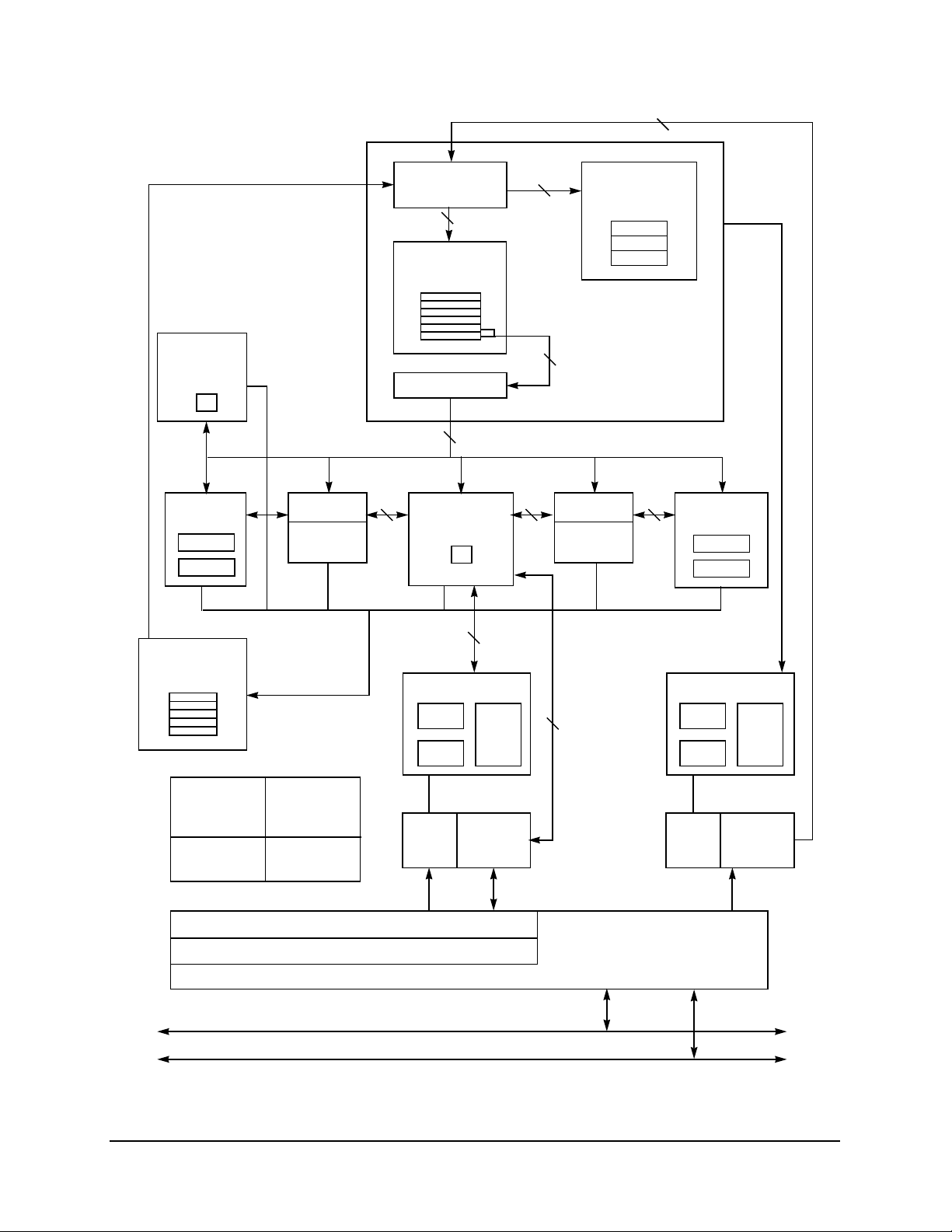
1.2 Block Diagram
Figure 1 provides a block diagram of the 603e that illustrates how the execution units—IU, FPU, BPU,
LSU, and SRU—operate independently and in parallel.
The 603e provides address translation and protection facilities, including an ITLB, DTLB, and instruction
and data BAT arrays. Instruction fetching and issuing is handled in the instruction unit. Translation of
addresses for cache or external memory accesses are handled by the MMUs. Both units are discussed in
more detail in Sections 1.3, “Instruction Unit,” and 1.5.1, “Memory Management Units (MMUs).”
1.3 Instruction Unit
As shown in Figure 1, the 603e instruction unit, which contains a sequential fetcher, instruction queue,
dispatch unit, and BPU, provides centralized control of instruction flow to the execution units. The
instruction unit determines the address of the next instruction to be fetched based on information from the
sequential fetcher and from the BPU.
The sequential fetcher fetches the instructions from the instruction cache into the instruction queue. The
BPU extracts branch instructions from the sequential fetcher and uses static branch prediction on unresolved
conditional branches to allow the instruction unit to fetch instructions from a predicted target instruction
stream while a conditional branch is evaluated. The BPU folds out branch instructions for unconditional
branches or conditional branches unaffected by instructions in progress in the execution pipeline.
Instructions issued beyond a predicted branch do not complete execution until the branch is resolved,
preserving the programming model of sequential execution. If any of these instructions are to be executed
in the BPU, they are decoded but not issued. Instructions to be executed by the FPU, IU, LSU, and SRU are
issued and allowed to complete up to the register write-back stage. Write-back is allowed when a correctly
predicted branch is resolved, and instruction execution continues without interruption along the predicted
path.
If branch prediction is incorrect, the instruction unit flushes all predicted path instructions, and instructions
are issued from the correct path.
PowerPC 603e RISC Microprocessor Technical Summary
Page 5
5
64 Bit
SYSTEM
REGISTER
UNIT
+
INTEGER
UNIT
+
/
*
XER
GPR File
GP Rename
Registers
SEQUENTIAL
FETCHER
64 Bit
INSTRUCTION
QUEUE
Dispatch Unit
64 Bit
LOAD/STORE
UNIT
+
64 Bit
64 Bit
BRANCH
PROCESSING
INSTRUCTION UNIT
64 Bit64 Bit
FPR File
FP Rename
Registers
UNIT
CTR
CR
LR
64 Bit
FLOATING-
POINT UNIT
+
/
*
FPSCR
COMPLETION
UNIT
Power
Dissipation
Control
JTAG/COP
Interface
Time Base
Counter/
Decrementer
Clock
Multiplier
Touch Load Buffer
Copyback Buffer
32 Bit
D MMU
SRs
DTLB
Tags
32-BIT ADDRESS BUS
32-/64-BIT DATA BUS
DBAT
Array
16-Kbyte
D Cache
64 Bit
PROCESSOR BUS
INTERFACE
SRs
ITLB
Tags
I MMU
IBAT
Array
16-Kbyte
I Cache
Figure 1. PowerPC 603e Microprocessor Block Diagram
PowerPC 603e RISC Microprocessor Technical Summary
Page 6

6
1.3.1 Instruction Queue and Dispatch Unit
The instruction queue (IQ), shown in Figure 1, holds as many as six instructions and loads up to two
instructions from the instruction unit during a single cycle. The instruction fetch unit continuously loads as
many instructions as space in the IQ allows. Instructions are dispatched to their respective execution units
from the dispatch unit at a maximum rate of two instructions per cycle. Dispatching is facilitated to the IU,
FPU, LSU, and SRU by the provision of a reservation station at each unit. The dispatch unit checks for
source and destination register dependencies, determines if dispatch serialization is required, and inhibits
subsequent instruction dispatching as required.
For a more detailed overview of instruction dispatch, see Section 2.7, “Instruction Timing.”
1.3.2 Branch Processing Unit (BPU)
The BPU receives branch instructions from the fetch unit and performs CR lookahead operations on
conditional branches to resolve them early, achieving the effect of a zero-cycle branch in many cases.
The BPU uses a bit in the instruction encoding to predict the direction of the conditional branch. Therefore,
when an unresolved conditional branch instruction is encountered, the 603e fetches instructions from the
predicted target stream until the conditional branch is resolved.
The BPU contains an adder to compute branch target addresses and three user-control registers—the link
register (LR), the count register (CTR), and the CR. The BPU calculates the return pointer for subroutine
calls and saves it into the LR for certain types of branch instructions. The LR also contains the branch target
address for the Branch Conditional to Link Register (
address for the Branch Conditional to Count Register (
can be copied to or from any GPR. Because the BPU uses dedicated registers rather than GPRs or FPRs,
execution of branch instructions is largely independent from execution of integer and floating-point
instructions.
bclr x ) instruction. The CTR contains the branch target
bcctr x ) instruction. The contents of the LR and CTR
1.4 Independent Execution Units
The PowerPC architecture’s support for independent execution units allows implementation of processors
with out-of-order instruction execution. For example, because branch instructions do not depend on GPRs
or FPRs, branches can often be resolved early, eliminating stalls caused by taken branches.
In addition to the BPU, the 603e provides four other execution units and a completion unit, which are
described in the following sections.
1.4.1 Integer Unit (IU)
The IU can execute all integer instructions. The IU executes one integer instruction at a time, performing
computations with its arithmetic logic unit (ALU) and XER register. Most integer instructions are singlecycle instructions. Thirty-two general-purpose registers are provided to support integer operations. Stalls
due to contention for GPRs are minimized by automatic allocation of the 5 rename registers. The 603e
writes the contents of the rename registers to the appropriate GPR when integer instructions are retired by
the completion unit.
1.4.2 Floating-Point Unit (FPU)
The FPU contains a single-precision multiply-add array and the floating-point status and control register
(FPSCR). The multiply-add array allows the 603e to efficiently implement multiply and multiply-add
operations. The FPU is pipelined so that one single- or double-precision instruction can be issued per clock
cycle. Thirty-two 64-bit floating-point registers are provided to support floating-point operations. Stalls due
to contention for FPRs are minimized by automatic allocation of the 4 rename registers. The 603e writes the
PowerPC 603e RISC Microprocessor Technical Summary
Page 7

contents of the rename registers to the appropriate FPR when floating-point instructions are retired by the
completion unit.
The 603e supports all IEEE 754 floating-point data types (normalized, denormalized, NaN, zero, and
infinity) in hardware, eliminating the latency incurred by software exception routines. (Note that exception
is also referred to as interrupt in the architecture specification.)
1.4.3 Load/Store Unit (LSU)
The LSU executes all load and store instructions and provides the data transfer interface between the GPRs,
FPRs, and the cache/memory subsystem. The LSU calculates effective addresses, performs data alignment,
and provides sequencing for load/store string and multiple instructions.
Load and store instructions are issued and translated in program order; however, the actual memory accesses
can occur out of order. Synchronizing instructions are provided to enforce strict ordering.
Cacheable loads, when free of data dependencies, execute in a speculative manner with a maximum
throughput of one per cycle and a two-cycle total latency . Data returned from the cache is held in a rename
register until the completion logic commits the value to a GPR or FPR. Stores cannot be executed out of
order and are held in the store queue until the completion logic signals that the store operation is to be
completed to memory. The 603e executes store instructions with a maximum throughput of one per cycle
and a three-cycle total latency. The time required to perform the actual load or store operation varies
depending on the processor/bus clock ratio, and whether the operation involves the cache, system memory ,
or an I/O device.
1.4.4 System Register Unit (SRU)
The SRU executes various system-level instructions, including condition register logical operations and
move to/from special-purpose register instructions, and also executes integer add/compare instructions. In
order to maintain system state, most instructions executed by the SRU are completion-serialized; that is, the
instruction is held for execution in the SRU until all prior instructions issued have completed. Results from
completion-serialized instructions executed by the SRU are not available or forwarded for subsequent
instructions until the instruction completes.
1.4.5 Completion Unit
The completion unit tracks instructions from dispatch through execution, and then retires, or “completes,”
them in program order. Completing an instruction commits the 603e to any architectural register changes
caused by that instruction. In-order completion ensures the correct architectural state when the 603e must
recover from a mispredicted branch or any exception.
Instruction state and other information required for completion is kept in a first-in-first-out (FIFO) queue of
five completion buffers. A single completion buffer entry is allocated for each instruction once it enters the
dispatch unit. A completion buffer entry is required for instruction dispatch; otherwise, instruction dispatch
stalls. A maximum of two instructions per cycle are completed in order from the queue.
1.5 Memory Subsystem Support
The 603e provides support for cache and memory management through dual instruction and data memory
management units. The 603e also provides dual 16-Kbyte instruction and data caches, and an efficient
processor bus interface for access into main memory and other bus subsystems. The memory subsystem
support functions are described in the following subsections.
PowerPC 603e RISC Microprocessor Technical Summary
7
Page 8

8
1.5.1 Memory Management Units (MMUs)
The 603e’s MMUs support up to 4 Petabytes (2
52
) of virtual memory and 4 Gigabytes (2
memory (referred to as real memory in the architecture specification) for instructions and data. The MMUs
also control access privileges for these spaces on block and page granularities. Referenced and changed
status is maintained by the processor for each page to assist implementation of a demand-paged virtual
memory system. A key bit is implemented to provide information about memory protection violations prior
to page table search operations.
The LSU calculates effective addresses for data loads and stores, performs data alignment to and from cache
memory, and provides the sequencing for load and store string and multiple word instructions. The
instruction unit calculates the effective addresses for instruction fetching.
The higher-order bits of the effective address are translated by the appropriate MMU into physical address
bits. Simultaneously, the lower-order address bits (that are untranslated and therefore, considered both
logical and physical) are directed to the on-chip caches where they form the index into the four-way setassociative tag array. After translating the address, the MMU passes the higher-order bits of the physical
address to the cache and the cache lookup completes. For caching-inhibited accesses or accesses that miss
in the cache, the untranslated lower-order address bits are concatenated with the translated higher-order
address bits; the resulting 32-bit physical address is used by the memory unit and the system interface,
which accesses external memory.
32
) of physical
The MMU also directs the address translation and enforces the protection hierarchy programmed by the
operating system in relation to the supervisor/user privilege level of the access and in relation to whether
the access is a load or store.
For instruction accesses, the MMU performs an address lookup in both the 64 entries of the ITLB, and in
the IBAT array. If an effective address hits in both the ITLB and the IBAT array, the IBAT array translation
takes priority. Data accesses cause a lookup in the DTLB and DBAT array for the physical address
translation. In most cases, the physical address translation resides in one of the TLBs and the physical
address bits are readily available to the on-chip cache.
When the physical address translation misses in the TLBs, the 603e provides hardware assistance for
software to perform a search of the translation tables in memory. The hardware assist consists of the
following features:
• Automatic storage of the missed effective address in the IMISS and DMISS registers
• Automatic generation of the primary and secondary hashed real address of the page table entry
group (PTEG), which are readable from the HASH1 and HASH2 register locations.
The HASH data is generated from the contents of the IMISS or DMISS register. Which register is
selected depends on which miss (instruction or data) was last acknowledged.
• Automatic generation of the first word of the page table entry (PTE) for which the tables are being
searched
• A real page address (RPA) register that matches the format of the lower word of the PTE
• Two TLB access instructions (
tlbli and tlbld ) that are used to load an address translation into the
instruction or data TLBs
• Shadow registers for GPR0–GPR3 that allow miss code to execute without corrupting the state of
any of the existing GPRs. These shadow registers are only used for servicing a TLB miss.
See Section 2.6.2, “PowerPC 603e Microprocessor Memory Management,” for more information about
memory management for the 603e.
PowerPC 603e RISC Microprocessor Technical Summary
Page 9

1.5.2 Cache Units
The 603e provides independent 16-Kbyte, four-way set-associative instruction and data caches. The cache
block is 32 bytes long. The caches adhere to a write-back policy, but the PowerPC architecture allows
control of cacheability, write policy, and memory coherency at the page and block levels. The caches use a
least recently used (LRU) replacement policy.
As shown in Figure 1, the caches provide a 64-bit interface to the instruction fetch unit and load/store unit.
The surrounding logic selects, organizes, and forwards the requested information to the requesting unit.
Write operations to the cache can be performed on a byte basis, and a complete read-modify-write operation
to the cache can occur in each cycle.
The load/store and instruction fetch units provide the caches with the address of the data or instruction to
be fetched. In the case of a cache hit, the cache returns two words to the requesting unit.
Since the 603e data cache tags are single ported, simultaneous load or store and snoop accesses cause
resource contention. Snoop accesses have the highest priority and are given first access to the tags, unless
the snoop access coincides with a tag write, in which case the snoop is retried and must re-arbitrate for
access to the cache. Loads or stores that are deferred due to snoop accesses are executed on the clock cycle
following the snoop.
1.6 Processor Bus Interface
Memory accesses can occur in single-beat (1–8 bytes) and four-beat burst (32 bytes) data transfers when the
bus is configured as 64 bits, and in single-beat (1–4 bytes), two-beat (8 bytes), and eight-beat (32 bytes) data
transfers when the bus is configured as 32 bits. The address and data buses operate independently to support
pipelining and split transactions during memory accesses. The 603e can pipeline its bus transactions to a
depth of one level.
Because the caches on the 603e are on-chip, write-back caches, the predominant type of transaction for most
applications is burst-read memory operations, followed by burst-write memory operations, and single-beat
(noncacheable or write-through) memory read and write operations. Additionally, there can be address-only
operations, variants of the burst and single-beat operations, (for example, global memory operations that are
snooped and atomic memory operations), and address retry activity (for example, when a snooped read
access hits a modified line in the cache).
Access to the system interface is granted through an external arbitration mechanism that allows devices to
compete for bus mastership. This arbitration mechanism is flexible, allowing the 603e to be integrated into
systems that implement various fairness and bus parking procedures to avoid arbitration overhead.
Typically, memory accesses are weakly ordered—sequences of operations, including load/store string and
multiple instructions, do not necessarily complete in the order they begin—maximizing the efficiency of the
bus without sacrificing coherency of the data. The 603e allows read operations to precede store operations
(except when a dependency exists, or in cases where a non-cacheable access is performed), and provides
support for a write operation to proceed a previously queued read data tenure (for example, allowing a snoop
push to be enveloped by the address and data tenures of a read operation). Because the processor can
dynamically optimize run-time ordering of load/store traffic, overall performance is improved.
1.7 System Support Functions
The 603e implements several support functions that include power management, time base/decrementer
registers for system timing tasks, an IEEE 1149.1(JTAG)/common on-chip processor (COP) test interface,
and a phase-locked loop (PLL) clock multiplier. These system support functions are described in the
following subsections.
PowerPC 603e RISC Microprocessor Technical Summary
9
Page 10

10
1.7.1 Power Management
The 603e provides four power modes selectable by setting the appropriate control bits in the machine state
register (MSR) and hardware implementation register 0 (HID0) registers. The four power modes are as
follows:
• Full-power–This is the default power state of the 603e. The 603e is fully powered and the internal
functional units are operating at the full processor clock speed. If the dynamic power management
mode is enabled, functional units that are idle will automatically enter a low-power state without
affecting performance, software execution, or external hardware.
• Doze–All the functional units of the 603e are disabled except for the time base/decrementer
registers and the bus snooping logic. When the processor is in doze mode, an external asynchronous
interrupt, a system management interrupt, a decrementer exception, a hard or soft reset, or machine
check brings the 603e into the full-power state. The 603e in doze mode maintains the PLL in a fully
powered state and locked to the system external clock input (SYSCLK) so a transition to the fullpower state takes only a few processor clock cycles.
• Nap–The nap mode further reduces power consumption by disabling bus snooping, leaving only the
time base register and the PLL in a powered state. The 603e returns to the full-power state upon
receipt of an external asynchronous interrupt, a system management interrupt, a decrementer
exception, a hard or soft reset, or a machine check input (MCP
a nap state takes only a few processor clock cycles.
). A return to full-power state from
• Sleep–Sleep mode reduces power consumption to a minimum by disabling all internal functional
units, after which external system logic may disable the PLL and SYSCLK. Returning the 603e to
the full-power state requires the enabling of the PLL and SYSCLK, followed by the assertion of an
external asynchronous interrupt, a system management interrupt, a hard or soft reset, or a machine
check input (MCP
) signal after the time required to relock the PLL.
1.7.2 Time Base/Decrementer
The time base is a 64-bit register (accessed as two 32-bit registers) that is incremented once every four bus
clock cycles; external control of the time base is provided through the time base enable (TBEN) signal. The
decrementer is a 32-bit register that can generate a maskable decrementer exception after a programmable
delay. The contents of the decrementer register are decremented once every four bus clock cycles, and the
decrementer exception is generated as the count passes through zero.
1.7.3 IEEE 1149.1 (JTAG)/COP Test Interface
The 603e provides IEEE 1149.1 and COP functions for facilitating board testing and chip debug. The IEEE
1149.1 test interface provides a means for boundary-scan testing the 603e and the board to which it is
attached. The COP function shares the IEEE 1149.1 test port, provides a means for executing test routines,
and facilitates chip and software debugging.
1.7.4 Clock Multiplier
The internal clocking of the 603e is generated from and synchronized to the external clock signal, SYSCLK,
by means of a voltage-controlled oscillator-based PLL. The PLL provides programmable internal processor
clock rates of 1x, 1.5x, 2x, 2.5x, 3x, 3.5x, and 4x multiples of the externally supplied clock frequency for
the PID6-603e, and multiples of 2x, 2.5x, 3x, 3.5x, 4x, 4.5x, 5x, 5.5x, and 6x of the externally provided
clock for the PID7v-603e. The bus clock is the same frequency and is synchronous with SYSCLK. The
configuration of the PLL can be read by software from hardware implementation register 1 (HID1).
PowerPC 603e RISC Microprocessor Technical Summary
Page 11

Part 2 PowerPC 603e Microprocessor:
Implementation
The PowerPC architecture is derived from the IBM POWER architecture (Performance Optimized with
Enhanced RISC architecture). The PowerPC architecture shares the benefits of the POWER architecture
optimized for single-chip implementations. The PowerPC architecture design facilitates parallel instruction
execution and is scalable to take advantage of future technological gains.
This section describes the PowerPC architecture in general, and specific details about the implementation
of the 603e as a low-power, 32-bit member of the PowerPC processor family.
• Features—Section 2.1, “Features,” describes general features that the 603e shares with the
PowerPC microprocessor family.
• Registers and programming model—Section 2.2, “PowerPC Registers and Programming Model,”
describes the registers for the operating environment architecture common among PowerPC
processors and describes the programming model. It also describes the additional registers that are
unique to the 603e.
• Instruction set and addressing modes—Section 2.3, “Instruction Set and Addressing Modes,”
describes the PowerPC instruction set and addressing modes for the PowerPC operating
environment architecture, and defines and describes the PowerPC instructions implemented in the
603e.
• Cache implementation—Section 2.4, “Cache Implementation,” describes the cache model that is
defined generally for PowerPC processors by the virtual environment architecture. It also provides
specific details about the 603e cache implementation.
• Exception model—Section 2.5, “Exception Model,” describes the exception model of the PowerPC
operating environment architecture and the differences in the 603e exception model.
• Memory management—Section 2.6, “Memory Management,” describes generally the conventions
for memory management among the PowerPC processors. This section also describes the 603e’s
implementation of the 32-bit PowerPC memory management specification.
• Instruction timing—Section 2.7, “Instruction Timing,” provides a general description of the
instruction timing provided by the superscalar, parallel execution supported by the PowerPC
architecture and the 603e.
• System interface—Section 2.8, “System Interface,” describes the signals implemented on the 603e.
2.1 Features
The 603e is a high-performance, superscalar PowerPC microprocessor. The PowerPC architecture allows
optimizing compilers to schedule instructions to maximize performance through efficient use of the
PowerPC instruction set and register model. The multiple, independent execution units allow compilers to
optimize instruction throughput. Compilers that take advantage of the flexibility of the PowerPC
architecture can additionally optimize system performance of the PowerPC processors.
The following sections summarize the features of the 603e, including both those that are defined by the
architecture and those that are unique to the 603e implementation.
The PowerPC architecture consists of the following layers, and adherence to the PowerPC architecture can
be measured in terms of which of the following levels of the architecture is implemented:
• PowerPC user instruction set architecture (UISA)—Defines the base user-level instruction set, userlevel registers, data types, floating-point exception model, memory models for a uniprocessor
environment, and programming model for a uniprocessor environment.
PowerPC 603e RISC Microprocessor Technical Summary
11
Page 12

12
• PowerPC virtual environment architecture (VEA)—Describes the memory model for a
multiprocessor environment, defines cache control instructions, and describes other aspects of
virtual environments. Implementations that conform to the VEA also adhere to the UISA, but may
not necessarily adhere to the OEA.
• PowerPC operating environment architecture (OEA)—Defines the memory management model,
supervisor-level registers, synchronization requirements, and the exception model.
Implementations that conform to the OEA also adhere to the UISA and the VEA.
The PowerPC architecture allows a wide range of designs for such features as cache and system interface
implementations. The 603e implementations support the three levels of the architecture described above.
For more information about the PowerPC architecture, see
Programming Environments
Specific features of the 603e are listed in Section 1.1, “PowerPC 603e Microprocessor Features.”
user’s manual.
PowerPC Microprocessor Family: The
2.2 PowerPC Registers and Programming Model
The PowerPC architecture defines register-to-register operations for most computational instructions.
Source operands for these instructions are accessed from the registers or are provided as immediate values
embedded in the instruction opcode. The three-register instruction format allows specification of a target
register distinct from the two source operands. Load and store instructions transfer data between registers
and memory.
PowerPC processors have two levels of privilege—supervisor mode of operation (typically used by the
operating system) and user mode of operation (used by the application software). The programming models
incorporate 32 GPRs, 32 FPRs, special-purpose registers (SPRs), and several miscellaneous registers. Each
PowerPC microprocessor also has its own unique set of hardware implementation (HID) registers.
Having access to privileged instructions, registers, and other resources allows the operating system to
control the application environment (providing virtual memory and protecting operating-system and critical
machine resources). Instructions that control the state of the processor, the address translation mechanism,
and supervisor registers can be executed only when the processor is operating in supervisor mode.
The following sections summarize the PowerPC registers that are implemented in the 603e.
2.2.1 General-Purpose Registers (GPRs)
The PowerPC architecture defines 32 user-level, general-purpose registers (GPRs). These registers are 32
bits wide in 32-bit PowerPC microprocessors and 64 bits wide in 64-bit PowerPC microprocessors. The
GPRs serve as the data source or destination for all integer instructions.
2.2.2 Floating-Point Registers (FPRs)
The PowerPC architecture also defines 32 user-level, 64-bit floating-point registers (FPRs). The FPRs serve
as the data source or destination for floating-point instructions. These registers can contain data objects of
either single- or double-precision floating-point formats.
2.2.3 Condition Register (CR)
The CR is a 32-bit user-level register that consists of eight four-bit fields that reflect the results of certain
operations, such as move, integer and floating-point compare, arithmetic, and logical instructions, and
provide a mechanism for testing and branching.
PowerPC 603e RISC Microprocessor Technical Summary
Page 13

(
2.2.4 Floating-Point Status and Control Register (FPSCR)
The floating-point status and control register (FPSCR) is a user-level register that contains all exception
signal bits, exception summary bits, exception enable bits, and rounding control bits needed for compliance
with the IEEE-754 standard.
2.2.5 Machine State Register (MSR)
The machine state register (MSR) is a supervisor-level register that defines the state of the processor. The
contents of this register are saved when an exception is taken and restored when the exception handling
completes. The 603e implements the MSR as a 32-bit register; 64-bit PowerPC processors implement a 64bit MSR.
2.2.6 Segment Registers (SRs)
For memory management, 32-bit PowerPC microprocessors implement sixteen 32-bit segment registers
(SRs). To speed access, the 603e implements the segment registers as two arrays; a main array (for data
memory accesses) and a shadow array (for instruction memory accesses). Loading a segment entry with the
Move to Segment Register
mtsr ) instruction loads both arrays.
2.2.7 Special-Purpose Registers (SPRs)
The PowerPC operating environment architecture defines numerous special-purpose registers that serve a
variety of functions, such as providing controls, indicating status, configuring the processor, and performing
special operations. During normal execution, a program can access the registers, shown in Figure 2,
depending on the program’s access privilege (supervisor or user, determined by the privilege-level (PR) bit
in the MSR). Note that registers such as the GPRs and FPRs are accessed through operands that are part of
the instructions. Access to registers can be explicit (that is, through the use of specific instructions for that
purpose such as Move to Special-Purpose Register (
mfspr ) instructions) or implicit, as the part of the execution of an instruction. Some registers are accessed
(
both explicitly and implicitly
In the 603e, all SPRs are 32 bits wide.
mtspr ) and Move from Special-Purpose Register
2.2.7.1 User-Level SPRs
The following 603e SPRs are accessible by user-level software:
• Link register (LR)—The link register can be used to provide the branch target address and to hold
the return address after branch and link instructions. The LR is 32 bits wide in 32-bit
implementations.
• Count register (CTR)—The CTR is decremented and tested automatically as a result of branch-andcount instructions. The CTR is 32 bits wide in 32-bit implementations.
• XER register—The 32-bit XER contains the summary overflow bit, integer carry bit, overflow bit,
and a field specifying the number of bytes to be transferred by a Load String Word Indexed (
or Store String Word Indexed (
stswx ) instruction.
lswx )
2.2.7.2 Supervisor-Level SPRs
The 603e also contains SPRs that can be accessed only by supervisor-level software. These registers consist
of the following:
• The 32-bit DSISR defines the cause of data access and alignment exceptions.
• The data address register (DAR) is a 32-bit register that holds the address of an access after an
alignment or DSI exception.
PowerPC 603e RISC Microprocessor Technical Summary
13
Page 14

14
rfi
rfi
• Decrementer register (DEC) is a 32-bit decrementing counter that provides a mechanism for
causing a decrementer exception after a programmable delay.
• The 32-bit SDR1 specifies the page table format used in virtual-to-physical address translation for
pages. (Note that physical address is referred to as real address in the architecture specification.)
• The machine status save/restore register 0 (SRR0) is a 32-bit register that is used by the 603e for
saving the address of the instruction that caused the exception, and the address to return to when a
Return from Interrupt (
) instruction is executed.
• The machine status save/restore register 1 (SRR1) is a 32-bit register used to save machine status
on exceptions and to restore machine status when an
instruction is executed.
• The 32-bit SPRG0–SPRG3 registers are provided for operating system use.
• The external access register (EAR) is a 32-bit register that controls access to the external control
facility through the External Control In Word Indexed (
Indexed (
ecowx ) instructions.
eciwx ) and External Control Out Word
• The time base register (TB) is a 64-bit register that maintains the time of day and operates interval
timers. The TB consists of two 32-bit fields—time base upper (TBU) and time base lower (TBL).
• The processor version register (PVR) is a 32-bit, read-only register that identifies the version
(model) and revision level of the PowerPC processor.
• Block address translation (BAT) arrays—The PowerPC architecture defines 16 BAT registers,
divided into four pairs of data BATs (DBATs) and four pairs of instruction BATs (IBATs). See
Figure 2 for a list of the SPR numbers for the BAT arrays.
The following supervisor-level SPRs are implementation-specific to the 603e:
• The DMISS and IMISS registers are read-only registers that are loaded automatically upon an
instruction or data TLB miss.
• The HASH1 and HASH2 registers contain the physical addresses of the primary and secondary
page table entry groups (PTEGs).
• The ICMP and DCMP registers contain a duplicate of the first word in the page table entry (PTE)
for which the table search is looking.
• The required physical address (RP A) register is loaded by the processor with the second word of the
correct PTE during a page table search.
• The hardware implementation (HID0 and HID1) registers provide the means for enabling the
603e’s checkstops and features, and allows software to read the configuration of the PLL
configuration signals.
• The instruction address breakpoint register (IABR) is loaded with an instruction address that is
compared to instruction addresses in the dispatch queue. When an address match occurs, an
instruction address breakpoint exception is generated.
Figure 2 shows all the 603e registers available at the user and supervisor level. The numbers to the right of
the SPRs indicate the number that is used in the syntax of the instruction operands to access the register.
PowerPC 603e RISC Microprocessor Technical Summary
Page 15

USER MODEL
General-Purpose
Registers
GPR31
Floating-Point
Registers
FPR31
Condition Register
GPR0
GPR1
FPR0
FPR1
CR
SUPERVISOR MODEL
Configuration Registers
Hardware
Implementation
Registers
1
SPR1 008HID0
SPR1 009HID1
Machine State
Register
MSR
Processor Version
Register
SPR 287PVR
Memory Management Registers
Instruction BAT
Registers
IBAT0L
IBAT1U
IBAT1L
IBAT2U
IBAT2L
IBAT3U
IBAT3L
SPR 528IBAT0U
SPR 529
SPR 530
SPR 531
SPR 532
SPR 533
SPR 534
SPR 535
Data BAT Registers
SPR 536DBAT0U
SPR 537DBAT0L
SPR 538DBAT1U
SPR 539DBAT1L
SPR 540DBAT2U
SPR 541DBAT2L
SPR 542DBAT3U
SPR 543DBAT3L
SDR1
SPR 25SDR1
Software Table
Search Registers
SPR 976DMISS
SPR 977DCMP
SPR 978HASH1
SPR 979HASH2
SPR 980IMISS
SPR 981ICMP
SPR 982RPA
Segment Registers
SR0
SR1
SR15
1
Floating-Point Status
and Control Register
FPSCR
XER
XER
SPR 1
Link Register
LR
SPR 8
Data Address Register
DAR
SPRGs
SPRG1
SPRG2
SPRG3
Count Register
CTR
SPR 9
Time Base Facility
(For Writing)
Time Base Facility
(For Reading)
TBL
TBU
1
These registers are 603e–specific registers. They may not be supported by other PowerPC processors.
TBR 268
TBR 269
TBU
Instruction Address
Breakpoint Register
Exception Handling Registers
DSISR
SPR 19
Save and Restore
SPR 272SPRG0
SPR 273
SPR 274
SPR 275
Miscellaneous Registers
Decrementer
SPR 284TBL
SPR 285
1
SPR 1010IABR
External Address
Register (Optional)
SRR0
SRR1
DEC
EAR
SPR 18DSISR
SPR 26
SPR 27
SPR 22
SPR 282
Figure 2. PowerPC 603e Microprocessor Programming Model—Registers
PowerPC 603e RISC Microprocessor Technical Summary
15
Page 16

2.3 Instruction Set and Addressing Modes
All PowerPC instructions are encoded as single-word (32-bit) opcodes. Instruction formats are consistent
among all instruction types, permitting efficient decoding to occur in parallel with operand accesses. This
fixed instruction length and consistent format greatly simplifies instruction pipelining.
2.3.1 PowerPC Instruction Set
The PowerPC instructions are divided into the following categories:
• Integer instructions—These include computational and logical instructions.
— Integer arithmetic instructions
— Integer compare instructions
— Integer logical instructions
— Integer rotate and shift instructions
• Floating-point instructions—These include floating-point computational instructions, as well as
instructions that affect the FPSCR.
— Floating-point arithmetic instructions
— Floating-point multiply/add instructions
— Floating-point rounding and conversion instructions
— Floating-point compare instructions
— Floating-point status and control instructions
• Load/store instructions—These include integer and floating-point load and store instructions.
— Integer load and store instructions
— Integer load and store multiple instructions
— Floating-point load and store
— Primitives used to construct atomic memory operations (lwarx and stwcx. instructions)
• Flow control instructions—These include branching instructions, condition register logical
instructions, trap instructions, and other instructions that affect the instruction flow.
— Branch and trap instructions
— Condition register logical instructions
• Processor control instructions—These instructions are used for synchronizing memory accesses
and management of caches, TLBs, and the segment registers.
— Move to/from SPR instructions
— Move to/from MSR
— Synchronize
— Instruction synchronize
— Order loads and stores
• Memory control instructions—These instructions provide control of caches, TLBs, and segment
registers.
— Supervisor-level cache management instructions
— User-level cache instructions
— Segment register manipulation instructions
— Translation lookaside buffer management instructions
16 PowerPC 603e RISC Microprocessor Technical Summary
Page 17

Note that this grouping of the instructions does not indicate which execution unit executes a particular
instruction or group of instructions.
Integer instructions operate on byte, half-word, and word operands. Floating-point instructions operate on
single-precision (one word) and double-precision (one double word) floating-point operands. The PowerPC
architecture uses instructions that are four bytes long and word-aligned. It provides for byte, half-word, and
word operand loads and stores between memory and a set of 32 GPRs. It also provides for word and doubleword operand loads and stores between memory and a set of 32 floating-point registers (FPRs).
Computational instructions do not modify memory. To use a memory operand in a computation and then
modify the same or another memory location, the memory contents must be loaded into a register, modified,
and then written back to the target location with distinct instructions.
PowerPC processors follow the program flow when they are in the normal execution state. However, the
flow of instructions can be interrupted directly by the execution of an instruction or by an asynchronous
event. Either kind of exception may cause one of several components of the system software to be invoked.
2.3.2 Calculating Effective Addresses
The effective address (EA) is the 32-bit address computed by the processor when executing a memory
access or branch instruction or when fetching the next sequential instruction.
The PowerPC architecture supports two simple memory addressing modes:
• EA = (rA|0) + offset (including offset = 0) (register indirect with immediate index)
• EA = (rA|0) + rB (register indirect with index)
These simple addressing modes allow efficient address generation for memory accesses. Calculation of the
effective address occurs in a single clock cycle.
For a memory access instruction, if the sum of the effective address and the operand length exceeds the
maximum effective address, the memory operand is considered to wrap around from the maximum effective
address to effective address 0.
Effective address computations for both data and instruction accesses use 32-bit unsigned binary arithmetic.
A carry from bit 0 is ignored in 32-bit implementations.
2.3.3 PowerPC 603e Microprocessor Instruction Set
The 603e instruction set is defined as follows:
• The 603e provides hardware support for all 32-bit PowerPC instructions.
• The 603e provides two implementation-specific instructions used for software table search
operations following TLB misses:
– Load Data TLB Entry (tlbld)
– Load Instruction TLB Entry (tlbli)
• The 603e implements the following instructions which are defined as optional by the PowerPC
architecture:
– External Control In Word Indexed (eciwx)
– External Control Out Word Indexed (ecowx)
– Floating Select (fsel)
– Floating Reciprocal Estimate Single-Precision (fres)
– Floating Reciprocal Square Root Estimate (frsqrte)
– Store Floating-Point as Integer Word (stfiwx)
PowerPC 603e RISC Microprocessor Technical Summary 17
Page 18

2.4 Cache Implementation
The following subsections describe the PowerPC architecture’s treatment of cache in general, and the 603especific implementation, respectively.
2.4.1 PowerPC Cache Characteristics
The PowerPC architecture does not define hardware aspects of cache implementations. For example, some
PowerPC processors, including the 603e, have separate instruction and data caches (Harvard architecture),
while others, such as the PowerPC 601 microprocessor, implement a unified cache.
PowerPC microprocessors control the following memory access modes on a page or block basis:
• Write-back/write-through mode
• Caching-inhibited mode
• Memory coherency
Note that in the 603e, a cache block is defined as eight words. The VEA defines cache management
instructions that provide a means by which the application programmer can affect the cache contents.
2.4.2 PowerPC 603e Microprocessor Cache Implementation
The 603e has two 16-Kbyte, four-way set-associative (instruction and data) caches. The caches are
physically addressed, and the data cache can operate in either write-back or write-through mode as specified
by the PowerPC architecture.
The data cache is configured as 128 sets of 4 blocks each. Each block consists of 32 bytes, two state bits,
and an address tag. The two state bits implement the three-state MEI (modified/exclusive/invalid) protocol.
Each block contains eight 32-bit words. Note that the PowerPC architecture defines the term block as the
cacheable unit. For the 603e, the block size is equivalent to a cache line. A block diagram of the data cache
organization is shown in Figure 3.
The instruction cache also consists of 128 sets of 4 blocks, and each block consists of 32 bytes, an address
tag, and a valid bit. The instruction cache may not be written to except through a block fill operation. The
instruction cache is not snooped, and cache coherency must be maintained by software. A fast hardware
invalidation capability is provided to support cache maintenance. The organization of the instruction cache
is very similar to the data cache shown in Figure 3.
Each cache block contains eight contiguous words from memory that are loaded from an 8-word boundary
(that is, bits A27–A31 of the effective addresses are zero); thus, a cache block never crosses a page
boundary. Misaligned accesses across a page boundary can incur a performance penalty.
The 603e’s cache blocks are loaded in four beats of 64 bits each when the 603e is configured with a 64-bit
data bus; when the 603e is configured with a 32-bit bus, cache block loads are performed with eight beats
of 32 bits each. The burst load is performed as “critical double-word first.” The data cache is blocked to
internal accesses until the load completes; the instruction cache allows sequential fetching during a cache
block load. The critical double word is simultaneously written to the cache and forwarded to the requesting
unit, thus minimizing stalls due to load delays.
18 PowerPC 603e RISC Microprocessor Technical Summary
Page 19

To ensure coherency among caches in a multiprocessor (or multiple caching-device) implementation, the
603e implements the MEI protocol. These three states, modified, exclusive, and invalid, indicate the state
of the cache block as follows:
• Modified—The cache block is modified with respect to system memory; that is, data for this address
is valid only in the cache and not in system memory.
• Exclusive—This cache block holds valid data that is identical to the data at this address in system
memory. No other cache has this data.
• Invalid—This cache block does not hold valid data.
Cache coherency is enforced by on-chip bus snooping logic. Since the 603e’s data cache tags are single
ported, a simultaneous load or store and snoop access represent a resource contention. The snoop access is
given first access to the tags. The load or store then occurs on the clock following the snoop.
128 Sets
Block 0
Block 1
Block 2
Block 3
Address Tag 0
Address Tag 1
Address Tag 2
Address Tag 3
State
State
State
State
Figure 3. Data Cache Organization
Words 0–7
Words 0–7
Words 0–7
Words 0–7
8 Words/Block
2.5 Exception Model
The following subsections describe the PowerPC exception model and the 603e implementation,
respectively.
2.5.1 PowerPC Exception Model
The PowerPC exception mechanism allows the processor to change to supervisor state as a result of external
signals, errors, or unusual conditions arising in the execution of instructions, and differ from the arithmetic
exceptions defined by the IEEE for floating-point operations. When exceptions occur, information about the
state of the processor is saved to certain registers and the processor begins execution at an address
(exception vector) predetermined for each exception. Processing of exceptions occurs in supervisor mode.
Although multiple exception conditions can map to a single exception vector, a more specific condition may
be determined by examining a register associated with the exception—for example, the DSISR and the
FPSCR. Additionally, some exception conditions can be explicitly enabled or disabled by software.
The PowerPC architecture requires that exceptions be handled in program order; therefore, although a
particular implementation may recognize exception conditions out of order, they are presented strictly in
order. When an instruction-caused exception is recognized, any unexecuted instructions that appear earlier
in the instruction stream, including any that have not yet entered the execute stage, are required to complete
before the exception is taken. Any exceptions caused by those instructions are handled first. Likewise,
PowerPC 603e RISC Microprocessor Technical Summary 19
Page 20

exceptions that are asynchronous and precise are recognized when they occur, but are not handled until the
instruction currently in the completion stage successfully completes execution or generates an exception,
and the completed store queue is emptied.
Unless a catastrophic condition causes a system reset or machine check exception, only one exception is
handled at a time. If, for example, a single instruction encounters multiple exception conditions, those
conditions are handled sequentially. After the exception handler handles an exception, the instruction
execution continues until the next exception condition is encountered. However, in many cases there is no
attempt to re-execute the instruction. This method of recognizing and handling exception conditions
sequentially guarantees that exceptions are recoverable.
Exception handlers should save the information stored in SRR0 and SRR1 early to prevent the program state
from being lost due to a system reset and machine check exception or to an instruction-caused exception in
the exception handler, and before enabling external interrupts.
The PowerPC architecture supports four types of exceptions:
• Synchronous, precise—These are caused by instructions. All instruction-caused exceptions are
handled precisely; that is, the machine state at the time the exception occurs is known and can be
completely restored. This means that (excluding the trap and system call exceptions) the address of
the faulting instruction is provided to the exception handler and that neither the faulting instruction
nor subsequent instructions in the code stream will complete execution before the exception is
taken. Once the exception is processed, execution resumes at the address of the faulting instruction
(or at an alternate address provided by the exception handler). When an exception is taken due to a
trap or system call instruction, execution resumes at an address provided by the handler.
• Synchronous, imprecise—The PowerPC architecture defines two imprecise floating-point
exception modes, recoverable and nonrecoverable. Even though the 603e provides a means to
enable the imprecise modes, it implements these modes identically to the precise mode (that is, all
enabled floating-point enabled exceptions are always precise on the 603e).
• Asynchronous, maskable—The external, SMI, and decrementer interrupts are maskable
asynchronous exceptions. When these exceptions occur, their handling is postponed until the next
instruction, and any exceptions associated with that instruction, completes execution. If there are
no instructions in the execution units, the exception is taken immediately upon determination of the
correct restart address (for loading SRR0).
• Asynchronous, nonmaskable—There are two nonmaskable asynchronous exceptions: system reset
and the machine check exception. These exceptions may not be recoverable, or may provide a
limited degree of recoverability. All exceptions report recoverability through the MSR[RI] bit.
2.5.2 PowerPC 603e Microprocessor Exception Model
As specified by the PowerPC architecture, all 603e exceptions can be described as either precise or
imprecise and either synchronous or asynchronous. Asynchronous exceptions (some of which are maskable)
are caused by events external to the processor’s execution; synchronous exceptions, which are all handled
precisely by the 603e, are caused by instructions. The 603e exception classes are shown in Table 1.
20 PowerPC 603e RISC Microprocessor Technical Summary
Page 21

Table 1. PowerPC 603e Microprocessor Exception Classifications
Synchronous/Asynchronous Precise/Imprecise Exception Type
Asynchronous, nonmaskable Imprecise Machine check
System reset
Asynchronous, maskable Precise External interrupt
Decrementer
System management interrupt
Synchronous Precise Instruction-caused exceptions
Although exceptions have other characteristics as well, such as whether they are maskable or nonmaskable,
the distinctions shown in Table 1 define categories of exceptions that the 603e handles uniquely. Note that
Table 1 includes no synchronous imprecise instructions. While the PowerPC architecture supports
imprecise handling of floating-point exceptions, the 603e implements these exception modes as precise
exceptions.
The 603e’s exceptions, and conditions that cause them, are listed in Table 2. Exceptions that are specific to
the 603e are indicated.
Table 2. Exceptions and Conditions
Exception
Type
Reserved 00000 —
System reset 00100 A system reset is caused by the assertion of either SRESET
Machine
check
DSI 00300 The cause of a DSI exception can be determined by the bit settings in the DSISR,
ISI 00400 An ISI exception is caused when an instruction fetch cannot be performed for any
Vector Offset
(hex)
00200 A machine check is caused by the assertion of the TEA
transaction, assertion of MCP
listed as follows:
1 Set if the translation of an attempted access is not found in the primary hash
table entry group (HTEG), or in the rehashed secondary HTEG, or in the range
of a DBAT register; otherwise cleared.
4 Set if a memory access is not permitted by the page or DBAT protection
mechanism; otherwise cleared.
5 Set by an eciwx or ecowx instruction if the access is to an address that is
marked as write-through, or execution of a load/store instruction that accesses
a direct-store segment.
6 Set for a store operation and cleared for a load operation.
11 Set if eciwx or ecowx is used and EAR[E] is cleared.
of the following reasons:
• The effective (logical) address cannot be translated. That is, there is a page
fault for this portion of the translation, so an ISI exception must be taken to load
the PTE (and possibly the page) into memory.
• The fetch access is to a direct-store segment (indicated by SRR1[3] set).
• The fetch access violates memory protection (indicated by SRR1[4] set). If the
key bits (Ks and Kp) in the segment register and the PP bits in the PTE are set
to prohibit read access, instructions cannot be fetched from this location.
Causing Conditions
, or an address or data parity error.
or HRESET.
signal during a data bus
PowerPC 603e RISC Microprocessor Technical Summary 21
Page 22

Table 2. Exceptions and Conditions (Continued)
Exception
Type
External
interrupt
Alignment 00600 An alignment exception is caused when the 603e cannot perform a memory
Program 00700 A program exception is caused by one of the following exception conditions, which
Vector Offset
(hex)
00500 An external interrupt is caused when MSR[EE] = 1 and the INT signal is asserted.
access for any of reasons described below:
• The operand of a floating-point load or store instruction is not word-aligned.
• The operand of lmw, stmw, lwarx, and stwcx. instructions are not aligned.
• The operand of a single-register load or store operation is not aligned, and the
603e is in little-endian mode. (PID6-603e only)
• The execution of a floating-point load or store instruction to a direct-store
segment.
• The operand of a load, store, load multiple, store multiple, load string, or store
string instruction crosses a segment boundary into a direct-store segment, or
crosses a protection boundary.
• Execution of a misaligned eciwx or ecowx instruction. (PID7v-603e only)
• The instruction is lmw, stmw, lswi, lswx, stswi, stswx and the 603e is in little-
endian mode.
• The operand of dcbz is in memory that is write-through-required or caching-
inhibited.
correspond to bit settings in SRR1 and arise during execution of an instruction:
• Floating-point enabled exception—A floating-point enabled exception condition
is generated when the following condition is met:
(MSR[FE0] | MSR[FE1]) & FPSCR[FEX] is 1.
FPSCR[FEX] is set by the execution of a floating-point instruction that causes
an enabled exception or by the execution of one of the “move to FPSCR”
instructions that results in both an exception condition bit and its corresponding
enable bit being set in the FPSCR.
• Illegal instruction—An illegal instruction program exception is generated when
execution of an instruction is attempted with an illegal opcode or illegal
combination of opcode and extended opcode fields (including PowerPC
instructions not implemented in the 603e), or when execution of an optional
instruction not provided in the 603e is attempted (these do not include those
optional instructions that are treated as no-ops).
• Privileged instruction—A privileged instruction type program exception is
generated when the execution of a privileged instruction is attempted and the
MSR register user privilege bit, MSR[PR], is set. In the 603e, this exception is
generated for mtspr or mfspr with an invalid SPR field if SPR[0] = 1 and
MSR[PR] = 1. This may not be true for all PowerPC processors.
• Trap—A trap type program exception is generated when any of the conditions
specified in a trap instruction is met.
Causing Conditions
Floatingpoint
unavailable
Decrementer 00900 The decrementer exception occurs when the most significant bit of the
Reserved 00A00–00BFF —
System call 00C00 A system call exception occurs when a System Call (sc) instruction is executed.
00800 A floating-point unavailable exception is caused by an attempt to execute a
floating-point instruction (including floating-point load, store, and move
instructions) when the floating-point available bit is disabled (MSR[FP] = 0).
decrementer (DEC) register transitions from 0 to 1. Must also be enabled with the
MSR[EE] bit.
22 PowerPC 603e RISC Microprocessor Technical Summary
Page 23

Table 2. Exceptions and Conditions (Continued)
Exception
Type
Trace 00D00 A trace exception is taken when MSR[SE] =1 or when the currently completing
Reserved 00E00 The 603e does not generate an exception to this vector. Other PowerPC
Reserved 00E10–00FFF —
Instruction
translation
miss
Data load
translation
miss
Data store
translation
miss
Instruction
address
breakpoint
Vector Offset
(hex)
instruction is a branch and MSR[BE] =1.
processors may use this vector for floating-point assist exceptions.
01000 An instruction translation miss exception is caused when an effective address for
an instruction fetch cannot be translated by the ITLB.
01100 A data load translation miss exception is caused when an effective address for a
data load operation cannot be translated by the DTLB.
01200 A data store translation miss exception is caused when an effective address for a
data store operation cannot be translated by the DTLB, or where a DTLB hit
occurs, and the change bit in the PTE must be set due to a data store operation.
01300 An instruction address breakpoint exception occurs when the address (bits 0–29)
in the IABR matches the next instruction to complete in the completion unit, and
the IABR enable bit (bit 30) is set.
Causing Conditions
System
management
interrupt
Reserved 01500–02FFF —
01400 A system management interrupt is caused when MSR[EE] = 1 and the SMI
signal is asserted.
input
2.6 Memory Management
The following subsections describe the memory management features of the PowerPC architecture, and the
603e implementation, respectively.
2.6.1 PowerPC Memory Management
The primary functions of the MMU are to translate logical (effective) addresses to physical addresses for
memory accesses and to provide access protection on blocks and pages of memory.
There are two types of accesses generated by the 603e that require address translation—instruction accesses,
and data accesses to memory generated by load, store, and cache control instructions.
The PowerPC MMU and exception model support demand-paged virtual memory. Virtual memory
management permits execution of programs larger than the size of physical memory; demand-paged implies
that individual pages are loaded into physical memory from system memory only when they are first
accessed by an executing program.
The hashed page table is a variable-sized data structure that defines the mapping between virtual page
numbers and physical page numbers. The page table size is a power of 2, and its starting address is a multiple
of its size.
PowerPC 603e RISC Microprocessor Technical Summary 23
Page 24

The page table contains a number of page table entry groups (PTEGs). A PTEG contains eight page table
entries (PTEs) of eight bytes each; therefore, each PTEG is 64 bytes long. PTEG addresses are entry points
for table search operations.
Address translations are enabled by setting bits in the MSR—MSR[IR] enables instruction address
translations and MSR[DR] enables data address translations.
2.6.2 PowerPC 603e Microprocessor Memory Management
The instruction and data memory management units in the 603e provide 4 Gbytes of logical address space
accessible to supervisor and user programs with a 4-Kbyte page size and 256-Mbyte segment size. BAT
block sizes range from 128 Kbyte to 256 Mbyte and are software selectable. In addition, the 603e uses an
interim 52-bit virtual address and hashed page tables for generating 32-bit physical addresses. The MMUs
in the 603e rely on the exception processing mechanism for the implementation of the paged virtual memory
environment and for enforcing protection of designated memory areas.
Instruction and data TLBs provide address translation in parallel with the on-chip cache access, incurring
no additional time penalty in the event of a TLB hit. A TLB is a cache of the most recently used page table
entries. Software is responsible for maintaining the consistency of the TLB with memory . The 603e’s TLBs
are 64-entry , two-way set-associative caches that contain instruction and data address translations. The 603e
provides hardware assist for software table search operations through the hashed page table on TLB misses.
Supervisor software can invalidate TLB entries selectively.
The 603e also provides independent four-entry BAT arrays for instructions and data that maintain address
translations for blocks of memory . These entries define blocks that can vary from 128 Kbytes to 256 Mbytes.
The BAT arrays are maintained by system software.
As specified by the PowerPC architecture, the hashed page table is a variable-sized data structure that
defines the mapping between virtual page numbers and physical page numbers. The page table size is a
power of 2, and its starting address is a multiple of its size.
Also as specified by the PowerPC architecture, the page table contains a number of page table entry groups
(PTEGs). A PTEG contains eight page table entries (PTEs) of eight bytes each; therefore, each PTEG is 64
bytes long. PTEG addresses are entry points for table search operations.
2.7 Instruction Timing
The 603e is a pipelined superscalar processor. A pipelined processor is one in which the processing of an
instruction is reduced into discrete stages. Because the processing of an instruction is broken into a series
of stages, an instruction does not require the entire resources of an execution unit. For example, after an
instruction completes the decode stage, it can pass on to the next stage, while the subsequent instruction can
advance into the decode stage. This improves the throughput of the instruction flow. For example, it may
take three cycles for a floating-point instruction to complete, but if there are no stalls in the floating-point
pipeline, a series of floating-point instructions can have a throughput of one instruction per cycle.
The instruction pipeline in the 603e has four major pipeline stages, described as follows:
• The fetch pipeline stage primarily involves retrieving instructions from the memory system and
determining the location of the next instruction fetch. Additionally, the BPU decodes branches
during the fetch stage and folds out branch instructions before the dispatch stage if possible.
24 PowerPC 603e RISC Microprocessor Technical Summary
Page 25

• The dispatch pipeline stage is responsible for decoding the instructions supplied by the instruction
fetch stage, and determining which of the instructions are eligible to be dispatched in the current
cycle. In addition, the source operands of the instructions are read from the appropriate register file
and dispatched with the instruction to the execute pipeline stage. At the end of the dispatch pipeline
stage, the dispatched instructions and their operands are latched by the appropriate execution unit.
• During the execute pipeline stage each execution unit that has an executable instruction executes
the selected instruction (perhaps over multiple cycles), writes the instruction's result into the
appropriate rename register, and notifies the completion stage that the instruction has finished
execution. In the case of an internal exception, the execution unit reports the exception to the
completion/writeback pipeline stage and discontinues instruction execution until the exception is
handled. The exception is not signaled until that instruction is the next to be completed. Execution
of most floating-point instructions is pipelined within the FPU allowing up to three instructions to
be executing in the FPU concurrently. The pipeline stages for the floating-point unit are multiply,
add, and round-convert. Execution of most load/store instructions is also pipelined. The load/store
unit has two pipeline stages. The first stage is for effective address calculation and MMU translation
and the second stage is for accessing the data in the cache.
• The complete/writeback pipeline stage maintains the correct architectural machine state and
transfers the contents of the rename registers to the GPRs and FPRs as instructions are retired. If
the completion logic detects an instruction causing an exception, all following instructions are
cancelled, their execution results in rename registers are discarded, and instructions are fetched
from the correct instruction stream.
A superscalar processor is one that issues multiple independent instructions into multiple pipelines allowing
instructions to execute in parallel. The 603e has five independent execution units, one each for integer
instructions, floating-point instructions, branch instructions, load/store instructions, and system register
instructions. The IU and the FPU each have dedicated register files for maintaining operands (GPRs and
FPRs, respectively), allowing integer calculations and floating-point calculations to occur simultaneously
without interference.
Because the PowerPC architecture can be applied to such a wide variety of implementations, instruction
timing among various PowerPC processors varies accordingly.
2.8 System Interface
The system interface is specific for each PowerPC microprocessor implementation.
The 603e provides a versatile system interface that allows for a wide range of implementations. The
interface includes a 32-bit address bus, a 32- or 64-bit data bus, and 56 control and information signals (see
Figure 4). The system interface allows for address-only transactions as well as address and data
transactions. The 603e control and information signals include the address arbitration, address start, address
transfer, transfer attribute, address termination, data arbitration, data transfer, data termination, and
processor state signals. Test and control signals provide diagnostics for selected internal circuits.
PowerPC 603e RISC Microprocessor Technical Summary 25
Page 26
ADDRESS ARBITRATION
DATA ARBITRATION
ADDRESS START
ADDRESS TRANSFER
TRANSFER ATTRIBUTE
ADDRESS TERMINATION
CLOCKS
603e
Vdd
Figure 4. System Interface
Vdd (I/O)
DATA TRANSFER
DATA TERMINATION
SYSTEM STATUS
PROCESSOR STATE
TEST AND CONTROL
The system interface supports bus pipelining, which allows the address tenure of one transaction to overlap
the data tenure of another. The extent of the pipelining depends on external arbitration and control circuitry.
Similarly, the 603e supports split-bus transactions for systems with multiple potential bus masters—one
device can have mastership of the address bus while another has mastership of the data bus. Allowing
multiple bus transactions to occur simultaneously increases the available bus bandwidth for other activity
and as a result, improves performance.
The 603e supports multiple masters through a bus arbitration scheme that allows various devices to compete
for the shared bus resource. The arbitration logic can implement priority protocols, such as fairness, and can
park masters to avoid arbitration overhead. The MEI protocol ensures coherency among multiple devices
and system memory. Also, the 603e's on-chip caches and TLBs and optional second-level caches can be
controlled externally.
The 603e’s clocking structure allows the bus to operate at integer and fractional multiples of the processor
cycle time.
The following sections describe the 603e bus support for memory and direct-store interface operations. Note
that some signals perform different functions depending upon the addressing protocol used.
2.8.1 Memory Accesses
The 603e’s data bus is configured at power-up to either a 32- or 64-bit width. When the 603e is configured
with a 32-bit data bus, memory accesses allow transfer sizes of 8, 16, 24, or 32 bits in one bus clock cycle.
Data transfers occur in either single-beat transactions, or two-beat or eight-beat burst transactions, with a
single-beat transaction transferring as many as 32 bits. Single- or double-beat transactions are caused by
noncached accesses that access memory directly (that is, reads and writes when caching is disabled,
caching-inhibited accesses, and stores in write-through mode). Eight-beat burst transactions, which always
transfer an entire cache line (32 bytes), are initiated when a line is read from or written to memory.
When the 603e is configured with a 64-bit data bus, memory accesses allow transfer sizes of 8, 16, 24, 32,
40, 48, 56, or 64 bits in one bus clock cycle. Data transfers occur in either single-beat transactions or fourbeat burst transactions. Single-beat transactions are caused by noncached accesses that access memory
directly (that is, reads and writes when caching is disabled, caching-inhibited accesses, and stores in writethrough mode). Four-beat burst transactions, which always transfer an entire cache line (32 bytes), are
initiated when a line is read from or written to memory.
26 PowerPC 603e RISC Microprocessor Technical Summary
Page 27

2.8.2 PowerPC 603e Microprocessor Signals
The 603e’s signals are grouped as follows:
• Address arbitration signals—The 603e uses these signals to arbitrate for address bus mastership.
• Address transfer start signals—These signals indicate that a bus master has begun a transaction on
the address bus.
• Address transfer signals—These signals, which consist of the address bus, address parity, and
address parity error signals, are used to transfer the address and to ensure the integrity of the
transfer.
• Transfer attribute signals—These signals provide information about the type of transfer , such as the
transfer size and whether the transaction is bursted, write-through, or caching-inhibited.
• Address transfer termination signals—These signals are used to acknowledge the end of the address
phase of the transaction. They also indicate whether a condition exists that requires the address
phase to be repeated.
• Data arbitration signals—The 603e uses these signals to arbitrate for data bus mastership.
• Data transfer signals—These signals, which consist of the data bus, data parity , and data parity error
signals, are used to transfer the data and to ensure the integrity of the transfer.
• Data transfer termination signals—Data termination signals are required after each data beat in a
data transfer. In a single-beat transaction, the data termination signals also indicate the end of the
tenure, while in burst accesses, the data termination signals apply to individual beats and indicate
the end of the tenure only after the final data beat. They also indicate whether a condition exists that
requires the data phase to be repeated.
• System status signals—These signals include the interrupt signal, checkstop signals, and both softand hard-reset signals. These signals are used to interrupt and, under various conditions, to reset the
processor.
• Processor state signals—These signals indicate the state of the reservation coherency bit, enable the
time base, provide machine power mode control, and cause a machine halt on execution of a tlbsync
instruction.
• IEEE 1149.1(JTAG)/COP interface signals—The IEEE 1149.1 test unit and the common on-chip
processor (COP) unit are accessed through a shared set of input, output, and clocking signals. The
IEEE 1149.1/COP interface provides a means for boundary scan testing and internal debugging of
the 603e.
• Test interface signals—These signals are used for production testing.
• Clock signals—These signals determine the system clock frequency . These signals can also be used
to synchronize multiprocessor systems.
NOTE
A bar over a signal name indicates that the signal is active low—for
example, AR
signals are referred to as asserted (active) when they are low and negated
when they are high. Signals that are not active low, such as AP0–AP3
(address bus parity signals) and TT0–TT4 (transfer type signals) are
referred to as asserted when they are high and negated when they are low.
TRY (address retry) and TS (transfer start). Active-low
PowerPC 603e RISC Microprocessor Technical Summary 27
Page 28
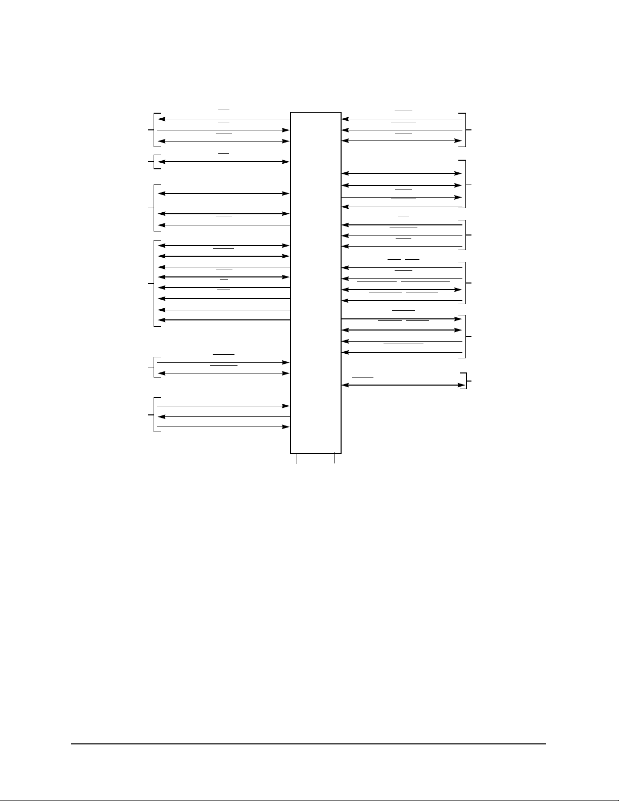
2.8.3 Signal Configuration
Figure 5 illustrates the 603e's logical pin configuration, showing how the signals are grouped.
ADDRESS
ARBITRATION
ADDRESS
START
ADDRESS
BUS
TRANSFER
ATTRIBUTE
ADDRESS
TERMINATION
CLOCKS
BR
BG
ABB
TS
A0–A31
AP0–AP3
APE
TT0–TT4
TBST
TSIZ0–TSIZ2
GBL
CI
WT
CSE0–CSE1
TC0–TC1
AACK
ARTRY
SYSCLK
CLK_OUT
PLL_CFG0 – PLL_CFG3
1
1
1
1
32
4
1
5
1
3
1
1
1
2
2
1
1
1
1
4
1
1
1
64
8
1
1
1
1
1
603e
2
1
2
2
1
2
1
1
5
DBG
DBWO
DBB
DH0–DH31, DL0–DL31
DP0–DP7
DPE
DBDIS
TA
DRTRY
TEA
INT, SMI
MCP
CKSTP_IN, CKSTP_OUT
HRESET, SRESET
RSRV
QREQ, QACK
TBEN
TLBISYNC
TRST, TCK, TMS, TDI, TD0
DATA
ARBITRATION
DATA
TRANSFER
DATA
TERMINATION
INTERRUPTS
CHECKSTOPS
RESET
PROCESSOR
STATUS
JTAG/COP
INTERFACE
Vdd (I/O)
Vdd
Figure 5. PowerPC 603e Microprocessor Signal Groups
2.9 PowerPC 603 and PowerPC 603e System Design
and Programming Considerations
The 603e is built upon the low power dissipation, low cost and high performance attributes of the 603 while
providing the system designer additional capabilities through higher processor clock speeds (to 166 MHz),
increases in cache size (16-Kbyte instruction and data caches) and set associativity (four-way), and greater
system clock flexibility. The following subsections describe the differences between the 603 and the 603e
that affect the system designer and programmer already familiar with the operation of the 603.
The design enhancements to the 603e are described in the following sections as changes that can require a
modification to the hardware or software configuration of a system designed for the 603.
28 PowerPC 603e RISC Microprocessor Technical Summary
Page 29

2.9.1 Hardware Features
The following hardware features of the 603e may require system designers to modify systems designed for
the 603.
2.9.1.1 Replacement of XATS Signal by CSE1 Signal
The 603e employs four-way set associativity for both the instruction and data caches, in place of the twoway set associativity used in the 603. This change requires the use of an additional cache set entry (CSE1)
signal to indicate which cache set is being loaded during a cache line fill. The CSE1 signal on the 603e is in
the same location as the XA
because support for access to direct-store segments has been removed. An attempt to access a direct-store
segment will result in a DSI exception.
Table 3 shows the CSE0–CSE1 signal encoding indicating the cache set selected during a cache load
operation.
TS signal on the 603. Note that the XA TS signal is no longer needed by the 603e
Table 3. CSE0–CSE1 Signals
CSE0–CSE1 Cache Set Element
00 Set 0
01 Set 1
10 Set 2
11 Set 3
2.9.1.2 Additional Bus Clock Multipliers
Some of the reserved clock configuration signal settings of the 603 are redefined to allow more flexible
selection of higher internal and bus clock frequencies. The PID6-603e provides additional bus clock
multipliers of 1.5/1, 2.5/1, and 3.5/1, and the PID7v-603e provides additional bus clock multipliers of 2.5/
1, 3.5/1, 4.5/1, 5/1, 5.5/1, and 6/1.
2.9.2 Software Features
The features of the 603e described in the following sections affect software originally written for the 603.
2.9.2.1 16-Kbyte Instruction and Data Caches
The instruction and data caches of the 603e are each 16 Kbytes in size, twice the size of the instruction and
data caches of the 603. The increase in cache size may require modification of cache flush routines. The
increase in cache size is also reflected in four-way set associativity of the instruction and data caches in place
of the two-way set associativity in the 603.
2.9.2.2 Direct-Store Operations
Unlike the 603, the 603e does not provide support for direct-store accesses. An attempt to access a directstore segment results in a DSI exception.
2.9.2.3 Clock Configuration Available in HID1 Register
Bits 0–3 in the new HID1 register (SPR 1009) provides software read-only access to the configuration of
the PLL_CFG signals. The HID1 register is not implemented in the 603.
PowerPC 603e RISC Microprocessor Technical Summary 29
Page 30

2.9.2.4 Performance Enhancements
The following enhancements provide improved performance on the 603e without any required changes to
software (other than compiler optimization) or hardware designed for the 603:
• Support for single-cycle store
• Support for instruction fetching from other instruction cache lines following the forwarding of the
critical first double word of a cache line load operation. Successive instruction fetches from the
cache line being loaded are forwarded, and accesses to other instruction cache lines can proceed
during the cache line load operation. (PID7v-603e only)
• Support for misaligned load and store operations in little-endian mode (PID7v-603e only)
• Addition of adder/comparator in system register unit allows dispatch and execution of multiple
integer add and compare instructions on each cycle
• Addition of a key bit (bit 12) to SRR1 to provide information about memory protection violations
prior to page table search operations. This key bit is set when the combination of the settings in the
appropriate Kx bit in the segment register and the MSR[PR] bit indicates that when the PP bits in
the PTE are set to either 00 or 01, a protection violation exists; if this is the case for a data write
operation with a DTLB miss, the changed (C) bit in the page tables should not be updated (see
T able 4). This reduces the time required to execute the page table search routine as the software no
longer has to explicitly read both the Kx and MSR[PR] bits to determine whether a protection
violation exists before updating the C bit.
Table 4. SRR1 [Key] Bit Generated by PowerPC 603e Microprocessor
Segment Register
[Ks, Kp]
0x 0 0
x0 1 0
1x 0 1
x1 1 1
Note that this key bit indicates a protection violation if the
PTE[pp] bits are either 00 or 01.
MSR[PR]
SRR1[Key] Generated
on DTLB Misses
30 PowerPC 603e RISC Microprocessor Technical Summary
Page 31

Information in this document is provided solely to enable system and software implementers to use PowerPC microprocessors. There are no express or
implied copyright or patent licenses granted hereunder by Motorola or IBM to design, modify the design of, or fabricate circuits based on the information in
this document.
The PowerPC 603e microprocessor embodies the intellectual property of Motorola and of IBM. However, neither Motorola nor IBM assumes any responsibility
or liability as to any aspects of the performance, operation, or other attributes of the microprocessor as marketed by the other party or by any third party. Neither
Motorola nor IBM is to be considered an agent or representative of the other, and neither has assumed, created, or granted hereby any right or authority to the
other, or to any third party, to assume or create any express or implied obligations on its behalf. Information such as data sheets, as well as sales terms and
conditions such as prices, schedules, and support, for the product may vary as between parties selling the product. Accordingly, customers wishing to learn more
information about the products as marketed by a given party should contact that party.
Both Motorola and IBM reserve the right to modify this document and/or any of the products as described herein without further notice. NOTHING IN THIS
DOCUMENT , NOR IN ANY OF THE ERRATA SHEETS, DATA SHEETS, AND OTHER SUPPORTING DOCUMENTATION, SHALL BE INTERPRETED AS THE
CONVEYANCE BY MOTOROLA OR IBM OF AN EXPRESS WARRANTY OF ANY KIND OR IMPLIED WARRANTY, REPRESENTATION, OR GUARANTEE
REGARDING THE MERCHANTABILITY OR FITNESS OF THE PRODUCTS FOR ANY PARTICULAR PURPOSE. Neither Motorola nor IBM assumes any
liability or obligation for damages of any kind arising out of the application or use of these materials. Any warranty or other obligations as to the products described
herein shall be undertaken solely by the marketing party to the customer, under a separate sale agreement between the marketing party and the customer . In the
absence of such an agreement, no liability is assumed by Motorola, IBM, or the marketing party for any damages, actual or otherwise.
“Typical” parameters can and do vary in different applications. All operating parameters, including “Typicals,” must be validated for each customer application
by customer’s technical experts. Neither Motorola nor IBM convey any license under their respective intellectual property rights nor the rights of others. Neither
Motorola nor IBM makes any claim, warranty, or representation, express or implied, that the products described in this document are designed, intended, or
authorized for use as components in systems intended for surgical implant into the body, or other applications intended to support or sustain life, or for any other
application in which the failure of the product could create a situation where personal injury or death may occur. Should customer purchase or use the products
for any such unintended or unauthorized application, customer shall indemnify and hold Motorola and IBM and their respective officers, employees, subsidiaries,
affiliates, and distributors harmless against all claims, costs, damages, and expenses, and reasonable attorney fees arising out of, directly or indirectly, any claim
of personal injury or death associated with such unintended or unauthorized use, even if such claim alleges that Motorola or IBM was negligent regarding the
design or manufacture of the part.
Motorola and are registered trademarks of Motorola, Inc. Motorola, Inc. is an Equal Opportunity/Affirmative Action Employer.
IBM, the IBM logo, and IBM Microelectronics are trademarks of International Business Machines Corporation.
The PowerPC name, the PowerPC logotype, PowerPC 601, PowerPC 603, and PowerPC 603e are trademarks of International Business Machines Corporation,
used by Motorola under license from International Business Machines Corporation. International Business Machines Corporation is an Equal Opportunity/
Affirmative Action Employer.
International Business Machines Corporation:
IBM Microelectronics Division, 1580 Route 52, Bldg. 504, Hopewell
Junction, NY 12533-6531; Tel. (800) PowerPC
World Wide Web Address: http://www.chips.ibm.com/products/ppc
http://www.ibm.com
Motorola Literature Distribution Centers:
USA/EUROPE: Motorola Literature Distribution; P.O. Box 20912; Phoenix, Arizona 85036;
Tel.: 1-800-441-2447
JAPAN: Nippon Motorola Ltd.; Tatsumi-SPD-JLDC, Toshikatsu Otsuki, 6F SeibuButsuryu-Center, 3-14-2 Tatsumi Koto-Ku, Tokyo 135, Japan; Tel.: 03-3521-8315
HONG KONG: Motorola Semiconductors H.K. Ltd.; 8B Tai Ping Industrial Park, 51 Ting
Kok Road, Tai Po, N.T., Hong Kong; Tel.: 852-26629298
MFAX: RMFAX0@email.sps.mot.com; TOUCHTONE (602) 244-6609
INTERNET: http://Design-NET.com
Technical Information: Motorola Inc. SPS Customer Support Center; (800) 521-6274.
Document Comments: FAX (512) 891-2638, Attn: RISC Applications Engineering.
World Wide Web Address: http://www.mot.com/powerpc/
 Loading...