

Motorola P2N2907A Datasheet
1
Motorola Small–Signal Transistors, FETs and Diodes Device Data
PNP Silicon
MAXIMUM RATINGS
Rating Symbol Value Unit
Collector–Emitter Voltage V
CEO
–60 Vdc
Collector–Base Voltage V
CBO
–60 Vdc
Emitter–Base Voltage V
EBO
–5.0 Vdc
Collector Current — Continuous I
C
–600 mAdc
Total Device Dissipation @ TA = 25°C
Derate above 25°C
P
D
625
5.0
mW
mW/°C
Total Device Dissipation @ TC = 25°C
Derate above 25°C
P
D
1.5
12
Watts
mW/°C
Operating and Storage Junction
Temperature Range
TJ, T
stg
–55 to +150 °C
THERMAL CHARACTERISTICS
Characteristic Symbol Max Unit
Thermal Resistance, Junction to Ambient
R
q
JA
200 °C/W
Thermal Resistance, Junction to Case
R
q
JC
83.3 °C/W
ELECTRICAL CHARACTERISTICS (T
A
= 25°C unless otherwise noted)
Characteristic
Symbol Min Max Unit
OFF CHARACTERISTICS
Collector–Emitter Breakdown Voltage
(1)
(IC = –10 mAdc, IB = 0)
V
(BR)CEO
–60 — Vdc
Collector–Base Breakdown Voltage
(IC = –10 mAdc, IE = 0)
V
(BR)CBO
–60 — Vdc
Emitter–Base Breakdown Voltage
(IE = –10 mAdc, IC = 0)
V
(BR)EBO
–5.0 — Vdc
Collector Cutoff Current
(VCE = –30 Vdc, V
EB(off)
= –0.5 Vdc)
I
CEX
— –50 nAdc
Collector Cutoff Current
(VCB = –50 Vdc, IE = 0)
(VCB = –50 Vdc, IE = 0, TA = 150°C)
I
CBO
—
—
–0.01
–10
µAdc
Emitter Cutoff Current
(VEB = –3.0 Vdc)
I
EBO
— –10 nAdc
Collector Cutoff Current
(VCE = –10 V)
I
CEO
— –10 nAdc
Base Cutoff Current
(VCE = –30 Vdc, V
EB(off)
= –0.5 Vdc)
I
BEX
— –50 nAdc
1. Pulse Test: Pulse Width v 300 ms, Duty Cycle v 2.0%.
Order this document
by P2N2907A/D
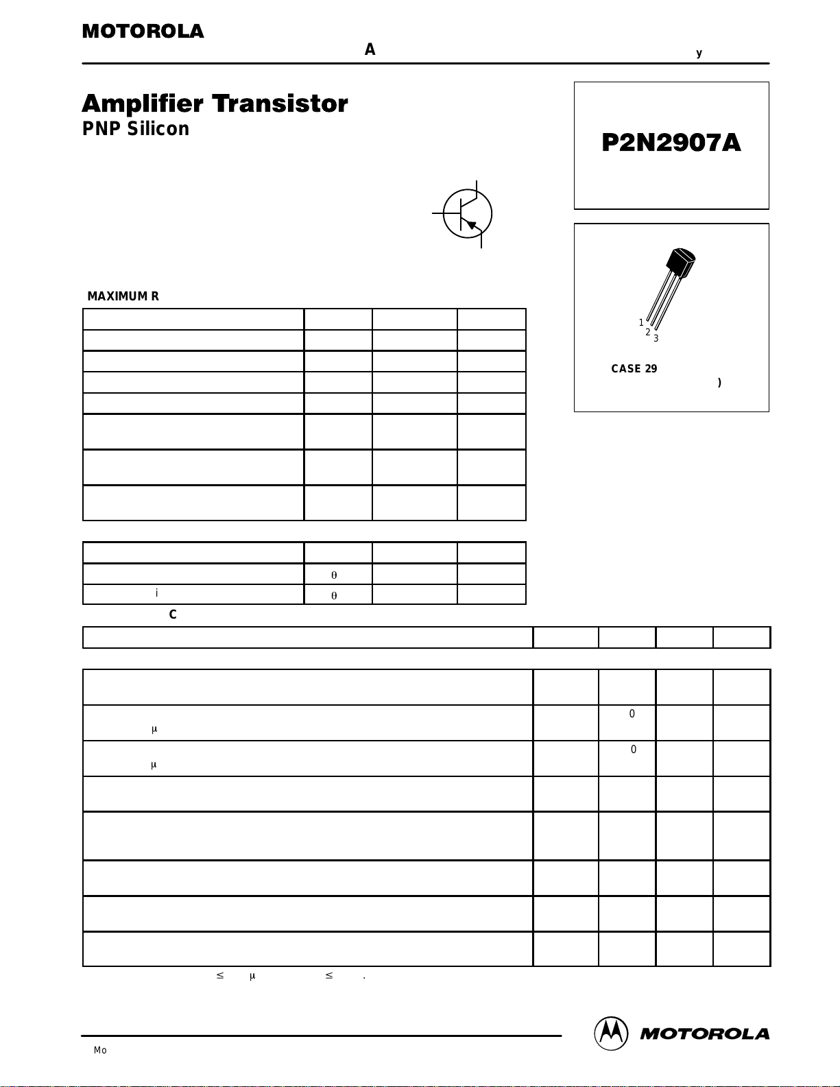
SEMICONDUCTOR TECHNICAL DATA
CASE 29–04, STYLE 17
TO–92 (TO–226AA)
1
2
3
Motorola, Inc. 1996
COLLECTOR
1
2
BASE
3
EMITTER
P2N2907A
2
Motorola Small–Signal Transistors, FETs and Diodes Device Data
ELECTRICAL CHARACTERISTICS
(TA = 25°C unless otherwise noted) (Continued)
Characteristic
Symbol Min Max Unit
ON CHARACTERISTICS
DC Current Gain
(IC = –0.1 mAdc, VCE = –10 Vdc)
(IC = –1.0 mAdc, VCE = –10 Vdc)
(IC = –10 mAdc, VCE = –10 Vdc)
(IC = –150 mAdc, VCE = –10 Vdc)
(1)
(IC = –500 mAdc, VCE = –10 Vdc)
(1)
h
FE
75
100
100
100
50
—
—
—
300
—
—
Collector–Emitter Saturation Voltage
(1)
(IC = –150 mAdc, IB = –15 mAdc)
(IC = –500 mAdc, IB = –50 mAdc)
V
CE(sat)
—
—
–0.4
–1.6
Vdc
Base–Emitter Saturation Voltage
(1)
(IC = –150 mAdc, IB = –15 mAdc)
(IC = –500 mAdc, IB = –50 mAdc)
V
BE(sat)
—
—
–1.3
–2.6
Vdc
SMALL–SIGNAL CHARACTERISTICS
Current–Gain — Bandwidth Product
(1), (2)
(IC = –50 mAdc, VCE = –20 Vdc, f = 100 MHz)
f
T
200 — MHz
Output Capacitance
(VCB = –10 Vdc, IE = 0, f = 1.0 MHz)
C
obo
— 8.0 pF
Input Capacitance
(VEB = –2.0 Vdc, IC = 0, f = 1.0 MHz)
C
ibo
— 30 pF
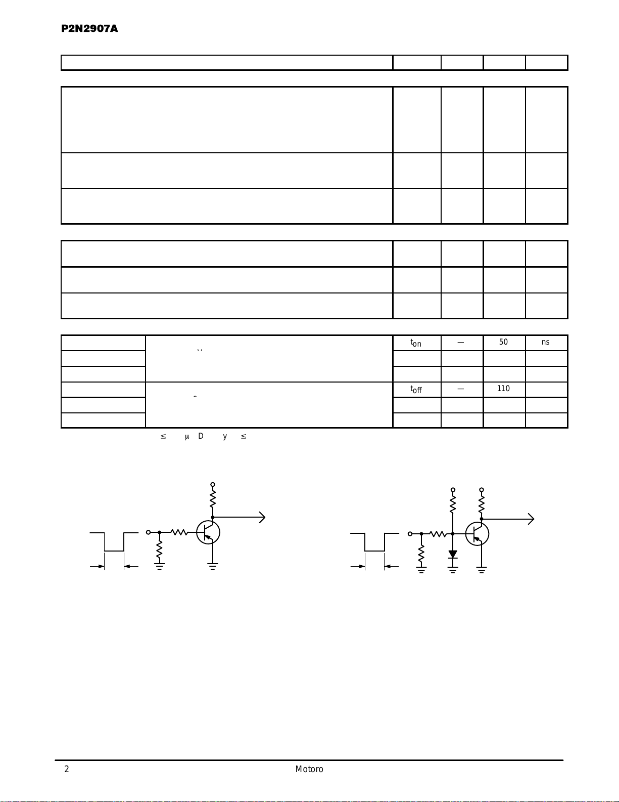
SWITCHING CHARACTERISTICS
Turn–On Time
t
on
— 50 ns
Delay Time
(VCC = –30 Vdc, IC = –150 mAdc,
I
= –15 mAdc) (Figures 1 and 5)
t
d
— 10 ns
Rise Time
IB1 = –15 mAdc) (Figures 1 and 5)
t
r
— 40 ns
Turn–Off Time
t
off
— 110 ns
Storage Time
(VCC = –6.0 Vdc, IC = –150 mAdc,
I
= I
= –15 mAdc) (Figure 2)
t
s
— 80 ns
Fall Time
IB1 = IB2 = –15 mAdc) (Figure 2)
t
f
— 30 ns
1. Pulse Test: Pulse Width v 300 ms, Duty Cycle v 2.0%.
2. fT is defined as the frequency at which |hfe| extrapolates to unity.
0
0
–16 V
200 ns
50
1.0 k
200
–30 V
TO OSCILLOSCOPE
RISE TIME
≤
5.0 ns
+15 V –6.0 V
1.0 k 37
50
1N916
1.0 k
200 ns
–30 V
TO OSCILLOSCOPE
RISE TIME
≤
5.0 ns
INPUT
Zo = 50
Ω
PRF = 150 PPS
RISE TIME
≤
2.0 ns
P.W. < 200 ns
INPUT
Zo = 50
Ω
PRF = 150 PPS
RISE TIME
≤
2.0 ns
P.W. < 200 ns
Figure 1. Delay and Rise Time Test Circuit Figure 2. Storage and Fall Time Test Circuit
 Loading...