Motorola NE556D, MC3456P Datasheet

Device
Operating
Temperature Range
Package
SEMICONDUCTOR
TECHNICAL DATA
DUAL TIMING CIRCUIT
ORDERING INFORMATION
MC3456P
NE556D
0° to +70°C
Plastic DIP
SO–14
PIN CONNECTIONS
Order this document by MC3456/D
P SUFFIX
PLASTIC PACKAGE
CASE 646
D SUFFIX
PLASTIC PACKAGE
CASE 751
(SO–14)
(Top View)
Discharge A
Threshold A
Control A
Reset A
Output A
Trigger A
Gnd
V
CC
Discharge B
Threshold B
Control B
Reset B
Output B
Trigger B
1
2
3
4
5
6
78
9
10
11
12
13
14
1
MOTOROLA ANALOG IC DEVICE DATA
The MC3456 dual timing circuit is a highly stable controller capable of
producing accurate time delays, or oscillation. Additional terminals are
provided for triggering or resetting if desired. In the time delay mode of
operation, the time is precisely controlled by one external resistor and
capacitor per timer. For astable operation as an oscillator, the free running
frequency and the duty cycle are both accurately controlled with two external
resistors and one capacitor per timer. The circuit may be triggered and reset
on falling waveforms, and the output structure can source or sink up to
200 mA or drive MTTL circuits.
• Direct Replacement for NE556/SE556 Timers
• Timing from Microseconds through Hours
• Operates in Both Astable and Monostable Modes
• Adjustable Duty Cycle
• High Current Output can Source or Sink 200 mA
• Output can Drive MTTL
• Temperature Stability of 0.005% per °C
• Normally “On” or Normally “Off” Output
• Dual Version of the Popular MC1455 Timer
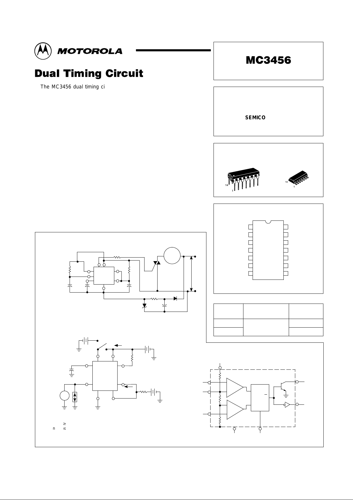
Figure 1. 22 Second Solid State Time Delay Relay Circuit
Figure 2. Block Diagram (1/2 Shown)
Figure 3. General Test Circuit
T est circuit for measuring DC parameters (to set output and measure parameters):
a) When VS w 2/3 VCC, VO is low.
b) When VS v1/3 VCC, VO is high.
c) When VO is low, Pin 7 sinks current. To test for Reset, set VO high,
c) apply Reset voltage, and test for current flowing into Pin 7. When Reset
c) is not in use, it should be tied to VCC.
1.0 k
Load
MT2
10 k
0.1
µ
F
0.01
µ
F
1
5
2
4
38
6
7
1.0
µ
FC
20 M
G
MT1
–10 V
1N4003
117 Vac/60 Hz
1N4740
3.5 k
250 V
–
+
t = 1.1; R and C = 22 sec
Time delay (t) is variable by
changing R and C (see Figure 16).
10 µF
V
CC
Threshold
Control Voltage
Trigger
2 (12)
3 (11)
6 (8)
5 k
14
5 k
5 k
+
–
Comp
A
+
–
Comp
B
7
Gnd Reset
4 (10)
R
S
Flip
Flop
Q
Inhibit/
Reset
1 (13)
5 (9)
Discharge
Output
R
1/2
MC3456
V
R
Reset 4 8
I
CC
V
CC
700
Discharge
6
Threshold
7
I
th
2.0 k
V
S
Trigger
2
Gnd
1
3
I
Sink
I
Source
V
O
0.01
µ
F
+
5
Control
Voltage
Output
V
CC
1/2
MC3456
Motorola, Inc. 1996 Rev 2

MC3456
2
MOTOROLA ANALOG IC DEVICE DATA
MAXIMUM RATINGS (T
A
= +25°C, unless otherwise noted.)
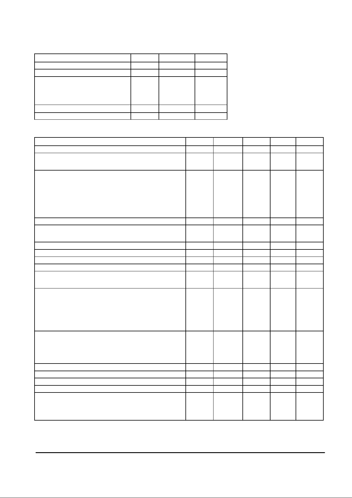
Rating Symbol Value Unit
Power Supply Voltage V
CC
+18 Vdc
Discharge Current I
dis
200 mA
Power Dissipation (Package Limitation)
P Suffix, Plastic Package, Case 646
Derate above TA = +25°C
D Suffix, Plastic Package, Case 751
Derate above TA = +25°C
P
D
625
5.0
1.0
8.0
mW
mW/°C
W
mW/°C
Operating Ambient T emperature Range T
A
0 to +70
°C
Storage Temperature Range T
stg
–65 to +150 °C
ELECTRICAL CHARACTERISTICS (T
A
= +25°C, VCC = +15 V, unless otherwise noted.)
Characteristics Symbol Min Typ Max Unit
Supply Voltage V
CC
4.5 – 16 V
Supply Current
VCC = 5.0 V, RL = ∞
VCC = 15 V, RL = ∞ Low State, (Note 1)
I
CC
–
–
6.0
20
12
30
mA
Timing Error (Note 2)
Monostable Mode (RA = 2.0 kΩ; C = 0.1 µF)
Initial Accuracy
Drift with T emperature
Drift with Supply Voltage
Astable Mode (RA = RB = 2.0 kΩ to 100 kΩ; C = 0.01 µF)
Initial Accuracy
Drift with T emperature
Drift with Supply Voltage
–
–
–
–
–
–
0.75
50
0.1
2.25
150
0.3
–
–
–
–
–
–
%
PPM/°C
%/V
%
PPM/°C
%/V
Threshold Voltage V
th
– 2/3 – xV
CC
Trigger V oltage
VCC = 15 V
VCC = 5.0 V
V
T
–
–
5.0
1.67
–
–
V
Trigger Current I
T
– 0.5 – µA
Reset Voltage V
R
0.4 0.7 1.0 V
Reset Current I
R
– 0.1 – mA
Threshold Current (Note 3) I
th
– 0.03 0.1 µA
Control Voltage Level
VCC = 15 V
VCC = 5.0 V
V
CL
9.0
2.6
10
3.33
11
4.0
V
Output Voltage Low
(VCC = 15 V)
I
Sink
= 10 mA
I
Sink
= 50 mA
I
Sink
= 100 mA
I
Sink
= 200 mA
(VCC = 5.0 V)
I
Sink
= 5.0 mA
V
OL
–
–
–
–
–
0.1
0.4
2.0
2.5
0.25
0.25
0.75
2.75
–
0.35
V
Output Voltage High
(I
Source
= 200 mA)
VCC = 15 V
(I
Source
= 100 mA)
VCC = 15 V
VCC = 5.0 V
V
OH
–
12.75
2.75
12.5
13.3
3.3
–
–
–
V
T oggle Rate RA = 3.3 kΩ, RB = 6.8 kΩ, C = 0.003 µF (Figure 17, 19) – – 100 – kHz
Discharge Leakage Current I
dis
– 20 100 nA
Rise Time of Output t
OLH
– 100 – ns
Fall Time of Output t
OHL
– 100 – ns
Matching Characteristics Between Sections
Monostable Mode
Initial Timing Accuracy
Timing Drift with Temperature
Drift with Supply Voltage
–
–
–
1.0
±10
0.2
2.0
–
0.5
%
ppm/°C
%/V
NOTES: 1. Supply current is typically 1.0 mA less for each output which is high.
2.Tested at VCC = 5.0 V and VCC = 15 V.
3.This will determine the maximum value of RA + RB for 15 V operation. The maximum total R = 20 mΩ.

MC3456
3
MOTOROLA ANALOG IC DEVICE DATA
25°C
I
Sink
(mA)
I
Sink
(mA)
VCC, SUPPLY VOLTAGE (Vdc)
I
Sink
(mA)
I
Source
(mA)
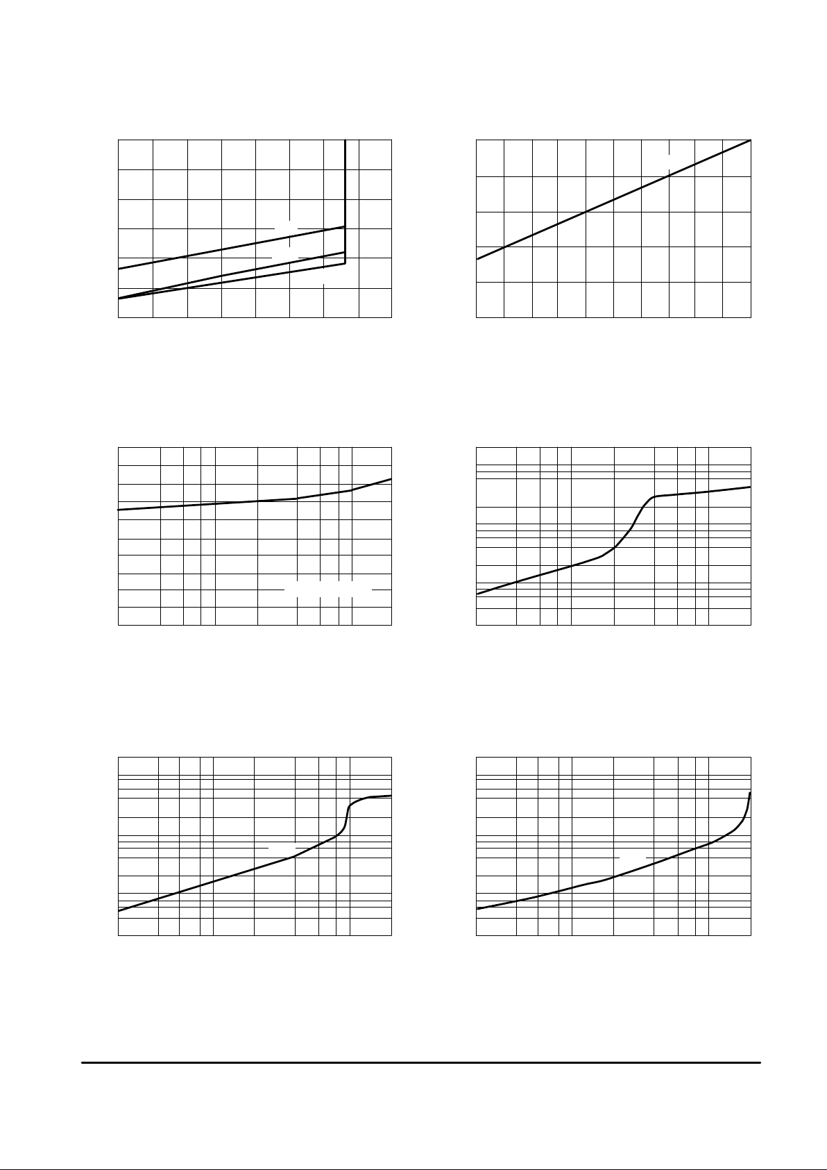
Figure 4. Trigger Pulse Width
V
T (min)
, MINIMUM TRIGGER VOLTAGE (X VCC = Vdc)
Figure 5. Supply Current
Figure 6. High Output Voltage
Figure 7. Low Output Voltage
(@ VCC = 5.0 Vdc)
Figure 8. Low Output Voltage
(@ VCC = 10 Vdc)
Figure 9. Low Output Voltage
(@ VCC = 15 Vdc)
0.4
150
125
100
75
50
25
0
PW, PULSE WIDTH (ns MIN)
I
CC
, SUPPLY CURRENT (mA)
1.0
1.0
V
CC
–V
OH
(Vdc)
V
OL
, (Vdc)
0.30.20.10
70°C
25°C
10
8.0
6.0
4.0
2.0
0
155.0 10
2.0
1.8
1.6
1.4
1.2
1.0
0.8
0.6
0.4
0.2
0
2.0 5.0 10 20 50 100
25°C
5.0 V ≤ VCC ≤ 15 V
10
1.0
0.1
0.01
1.0 2.0 5.0 10 20 50 100
2.0 5.0 10 20 50 100
10
1.0
0.1
0.01
1.0
2.0 5.0 10 20 50 100
10
1.0
0.1
0.01
25°C
0°C
25°C
V
OL
, (Vdc)
V
OL
, (Vdc)
25°C
 Loading...