© Semiconductor Components Industries, LLC, 2007
April, 2007 − Rev. 3
1 Publication Order Number:
NCP5663/D
NCP5663, NCV5663
Low Output Voltage,
Ultra−Fast 3.0 A Low Dropout
Linear Regulator with Enable
The NCP5663/NCV5663 is a high performance, low dropout linear
regulator designed for high power applications that require up to 3.0 A
current. It is offered in both fixed and adjustable output versions. With
output voltages as low as 0.9 V and ultra−fast response times for load
transients, the NCP5663/NCV5663 also provides additional features
such as Enable and Error Flag (for the fixed output version),
increasing the utility of this device. A thermally robust, 5 pin D
2
PAK,
combined with an architecture that offers low ground current
(independent of load), provides for a superior high−current LDO
solution.
Features
• Ultra−Fast Transient Response (Settling Time: 1−3 ms)
• Low Noise Without Bypass Capacitor (28 mV
rms)
• Low Ground Current Independent of Load (3.0 mA Maximum)
• Fixed/Adjustable Output Voltage Versions
• Enable Function
• Error Flag (Fixed Output Version)
• Current Limit Protection
• Thermal Protection
• 0.9 V Reference Voltage for Ultra−Low Output Operation
• Power Supply Rejection Ratio > 65 dB
• NCV Prefix for Automotive and Other Applications Requiring Site
and Control Changes
• This is a Pb−Free Device
Applications
• Servers
• ASIC Power Supplies
• Post Regulation for Power Supplies
• Constant Current Source
• Networking Equipment
• Gaming and STB Modules
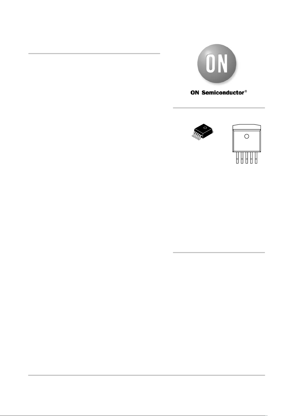
D2PAK
CASE 936A
1
5
x = P or V
y = A for Adjustable Version
B for Fixed 1.5 V Version
C for Fixed 1.8 V Version
A = Assembly Location
W = Wafer Lot
Y = Year
WW = Work Week
G = Pb−Free
MARKING
DIAGRAM
x5663DSy
AWYYWWG
Tab = Ground
Pin 1. Enable
2. V
in
3. Ground
4. V
out
5. Adj (adjustable output)
5. Error Flag (fixed output)
http://onsemi.com
MARKING
DIAGRAM
See detailed ordering and shipping information in the package
dimensions section on page 11 of this data sheet.
ORDERING INFORMATION
1
NC

NCP5663, NCV5663
http://onsemi.com
2
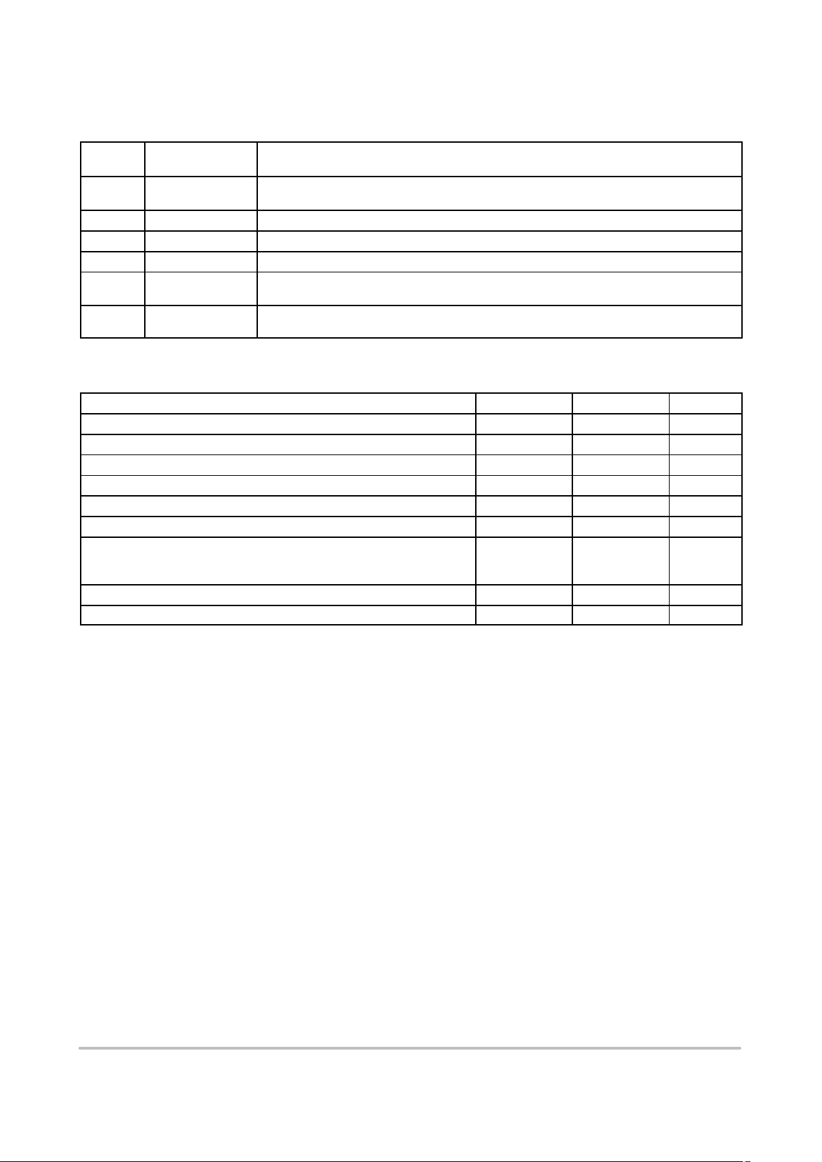
PIN FUNCTION DESCRIPTION
Pin
Adj/Fixed
Pin Name Description
1 Enable This pin allows for on/off control of the regulator. To disable the device, connect to Ground. If this
function is not in use, connect to V
in
.
2 V
in
Positive Power Supply Input Voltage
3 Ground Power Supply Ground
4 V
out
Regulated Output Voltage
5 Adj
(Adjustable Version)
This pin is connected to the resistor divider network and programs the output voltage.
5 Error Flag
(Fixed Version)
An Error Flag is triggered when the output voltage is out of regulation excluding transient signals
that may occur. Requires a pullup resistor f 100 kW.
ABSOLUTE MAXIMUM RATINGS
Rating Symbol Value Unit
Input Voltage (Note 1) V
in
18 V
Output Pin Voltage V
out
−0.3 to Vin +0.3 V
Adjust Pin Voltage V
adj
−0.3 to Vin +0.3 V
Enable Pin Voltage V
en
−0.3 to Vin +0.3 V
Error Flag Voltage V
ef
−0.3 to Vin +0.3 V
Error Flag Current I
ef
3.0 mA
Thermal Characteristics (Note 1)
Thermal Resistance Junction−to−Air (Note 2)
Thermal Resistance Junction−to−Case
R
θ
JA
R
θ
JC
45
5.0
°C/W
Operating Junction Temperature Range T
J
−40 to +150 °C
Storage Temperature Range T
stg
−55 to +150 °C
Stresses exceeding Maximum Ratings may damage the device. Maximum Ratings are stress ratings only. Functional operation above the
Recommended Opera t i n g Conditions is not implied. Extended exposure to stresses above the Recommended Operating Conditions may affect
device reliability.
NOTE: This device series contains ESD protection and exceeds the following tests:
Human Body Model (HBM) JESD 22−A114−B
Machine Model (MM) JESD 22−A115−A.
1. Refer to Electrical Characteristics table and Application Information section for Safe Operating Area.
2. As measured using a copper heat spreading area of 625 mm
2
, 1 oz. copper thickness.

NCP5663, NCV5663
http://onsemi.com
3
ELECTRICAL CHARACTERISTICS
(V
in
− V
out
= 1.5 V, for typical values TJ = 25°C, for min/max values TJ = −40°C to 85°C (125°C for NCV versions), Cin = C
out
= 150 mF
unless otherwise noted.)
Characteristic
Symbol Min Typ Max Unit
ADJUSTABLE OUTPUT VERSION
Input Voltage V
in
2.0 − 9.0 V
Output Noise Voltage V
n
− 28 −
mV
rms
Output Voltage Accuracy
T
J
= 25°C (V
in
= V
out
+1.5 V to 7.0 V, I
out
= 10 mA to 3.0 A)
T
J
= −20 to +125°C (V
in
= V
out
+1.5 V to 7.0 V, I
out
= 10 mA to 3.0 A)
T
J
= −40 to +150°C (V
in
= V
out
+1.5 V to 7.0 V, I
out
= 10 mA to 3.0 A)
V
out
−1%
−1.5%
−2%
−
0.9
−
+1%
+1.5%
+2%
V
Adjustable Pin Input Current I
adj
− 40 − nA
Line Regulation (I
out
= 10 mA, V
out
+1.5 V < Vin < 7.0 V) REG
line
− 0.03 − %
Load Regulation (10 mA < I
out
< 3.0 A) REG
load
− 0.03 − %
Dropout Voltage (I
out
= 3.0 A) V
DO
− 1.0 1.3 V
Peak Output Current Limit I
out
3.0 − − A
Internal Current Limitation I
lim
− 4.5 − A
Ripple Rejection (120 Hz)
Ripple Rejection (1 kHz)
RR −
−
70
65
−
−
dB
Thermal Shutdown (Guaranteed by Design) T
SHD
− 160 − °C
Ground Current
I
out
= 3.0 A
Disabled State
I
q
I
qds
−
−
1.3
10
3.0
300
mA
mA
Enable Input Threshold Voltage
Voltage Increasing, On state, Logic High
Voltage Decreasing, Off state, Logic Low
V
en
1.3
−
−
−
−
0.3
V
Enable Input Current
Enable Pin Voltage = 0.3 V
max
Enable Pin Voltage = 1.3 V
min
I
en
−
−
0.5
0.5
−
−
mA

NCP5663, NCV5663
http://onsemi.com
4
ELECTRICAL CHARACTERISTICS
(V
in
− V
out
= 1.5 V, for typical values TJ = 25°C, for min/max values TJ = −40°C to 85°C (125°C for NCV versions), Cin = C
out
= 150 mF
unless otherwise noted.)
Characteristic
Symbol Min Typ Max Unit
FIXED OUTPUT VOLTAGE
Input Voltage
V
in
2.0 − 9.0 V
Output Noise Voltage (V
out
= 0.9 V) V
n
− 28 −
mV
rms
Output Voltage Accuracy (Note 3)
T
J
= 25°C (V
in
= V
out
+1.5 V to 7.0 V, I
out
= 10 mA to 3.0 A)
T
J
= −20 to +125°C (V
in
= V
out
+1.5 V to 7.0 V, I
out
= 10 mA to 3.0 A)
T
J
= −40 to +150°C (V
in
= V
out
+1.5 V to 7.0 V, I
out
= 10 mA to 3.0 A)
V
out
−1%
−1.5%
−2%
−
V
out
−
+1%
+1.5%
+2%
V
Line Regulation (I
out
= 10 mA, V
out
+1.5 V < Vin < 7.0 V) REG
line
− 0.03 − %
Load Regulation (10 mA < I
out
< 3.0 A) REG
load
− 0.2 − %
Dropout Voltage (I
out
= 3.0 A) V
DO
− 1.0 1.3 V
Peak Output Current Limit I
out
3.0 − − A
Internal Current Limitation I
lim
− 4.5 − A
Ripple Rejection (120 Hz)
Ripple Rejection (1 kHz)
RR −
−
70
65
−
−
dB
Thermal Shutdown (Guaranteed by Design) T
SHD
− 160 − °C
Ground Current
I
out
= 3.0 A
Disabled State
I
q
I
qds
−
−
1.3
30
3.0
300
mA
mA
Enable Input Threshold Voltage
Voltage Increasing, On state, Logic High
Voltage Decreasing, Off state, Logic Low
V
en
1.3
−
−
−
−
0.3
V
Enable Input Current
Enable Pin Voltage = 0.3 V
max
Enable Pin Voltage = 1.3 V
min
I
en
−
−
0.5
0.5
−
−
mA
Error Flag (Fixed Output) V
cflt
91 94 97 % of V
out
Error Flag Output Low Voltage Saturation (Ief = 1.0 mA) V
cfdo
− 200 − mV
Error Flag Leakage I
efleak
− 1.0 −
mA
Error Flag Blanking Time (Note 4) T
ef
− 50 −
ms
3. Refer to Ordering Information Table for available voltage options.
4. Can be disabled per customer request.
 Loading...