MOTOROLA NCS6416DWG, NCS6416 Datasheet

NCS6416
Low-Voltage,
Bus-Contr olled Video
Matrix Switch
Description
The main function of the NCS6416 is to switch 8 video input
sources to the 6 outputs. The NCS6416 operates with a low 5 V power
supply.
Each output can be switched to only one of the inputs, whereas any
single input may be connected to several outputs.
All switching possibilities are controlled through the I2C bus inputs.
Features
•20 MHz Bandwidth
•5 V Operating Voltage
•Cascadable with another NCS6416 (Internal Address can be changed
by Pin 7 Voltage)
•8 Inputs (CVBS, RGB, Chroma, ...)
•6 Outputs with 150 Output Driving Capability
•Possibility of Chroma Signal for each Input by Switching off the
Clamp with an External Resistor Bridge
•Bus Controlled
•6 dB Gain between any Input and Output
•-65 dB Crosstalk at 5 MHz
•Full ESD Protection
•These are Pb-Free Devices
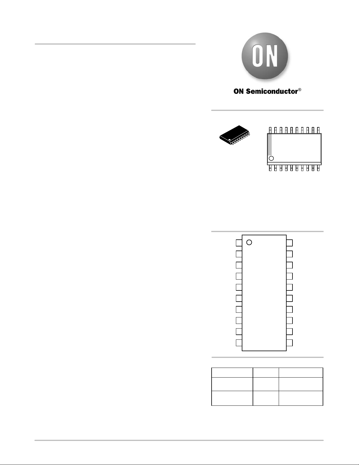
http://onsemi.com
MARKING DIAGRAMS*
20
20
1
SO-20 WB
DW SUFFIX
CASE 751D
A = Assembly Location
WL = Wafer Lot
YY = Year
WW = Work Week
G = Pb-Free Package
*For additional marking information, refer to
Application Note AND8002/D.
INPUT1
DATA1
INPUT2
CLOCK
1
2
3
4
1
NCS6416
AWLYYWWG
20
19
18
17
INPUT8
V
CCO
OUTPUT6
OUTPUT5
© Semiconductor Components Industries, LLC, 2007
June, 2007 - Rev. 1
INPUT3
INPUT4
PROG
INPUT5
V
CC
INPUT6
5
6
7
8
9
10
OUTPUT4
16
OUTPUT3
15
14
OUTPUT2
13
OUTPUT1
12
GND
INPUT7
11
ORDERING INFORMATION
Device Package Shipping
NCS6416DWG SO-20
(Pb-Free)
NCS6416DWR2G SO-20
(Pb-Free)
†For information on tape and reel specifications,
including part orientation and tape sizes, please
refer to our Tape and Reel Packaging Specifications
Brochure, BRD8011/D.
1 Publication Order Number:
38 Units / Rail
1000 / Tape & Reel
†
NCS6416/D

NCS6416
INPUT1
INPUT2
INPUT3
INPUT4
INPUT5
INPUT6
INPUT7
INPUT8
1
3
5
6
8
10
11
20
OUTPUT6
OUTPUT5
18 17 16 15 14 13 12
OUTPUT4
OUTPUT3
OUTPUT2
OUTPUT1
GND
Bus Decoder
274919
CLOCKPROGDATA
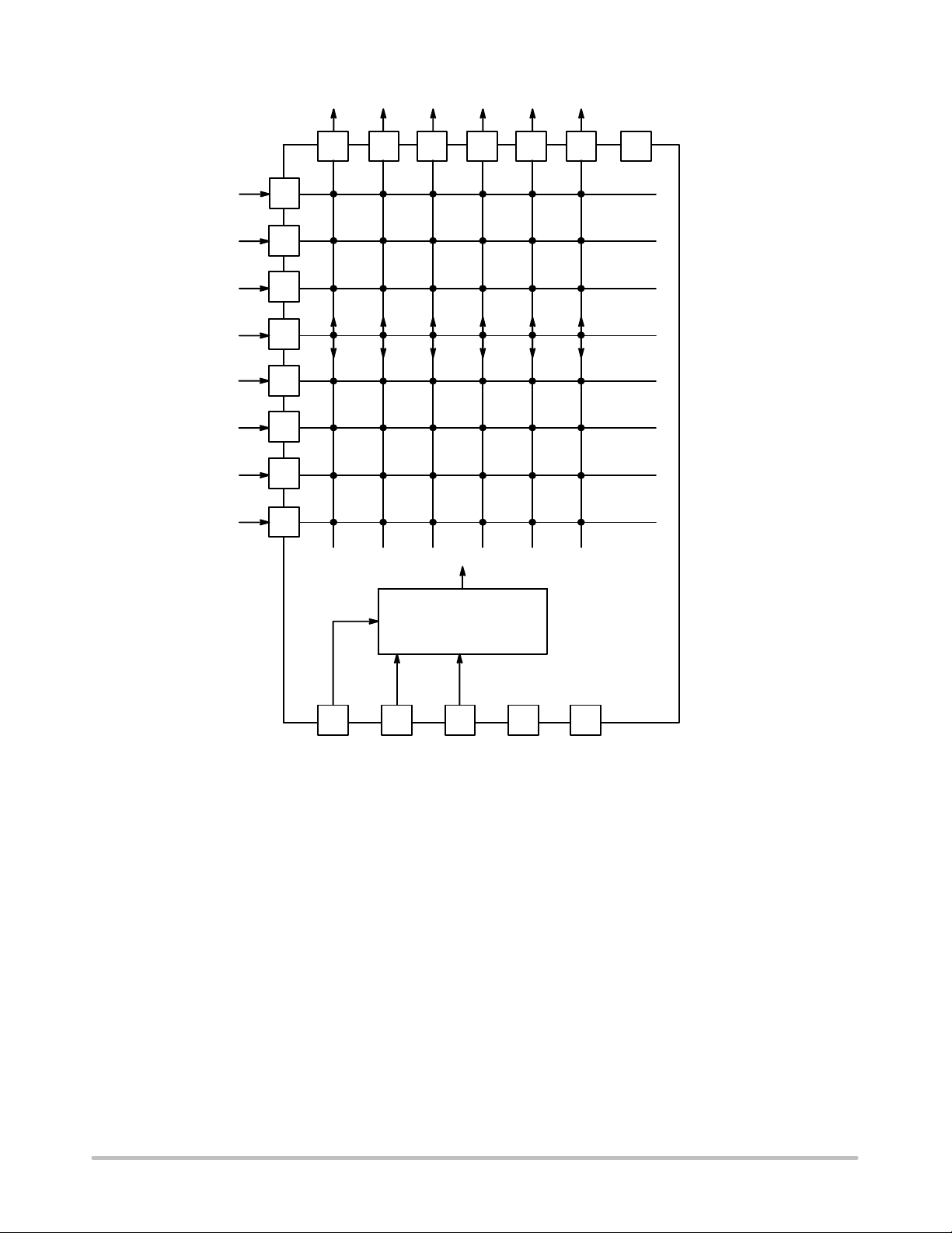
Figure 1. Block Diagram
The main function of the NCS6416 is to switch 8 video
input sources to the 6 outputs.
Each output can be switched to only one of the inputs,
whereas any single input may be connected to several
outputs. The lowest level of each signal is aligned on each
input (bottom of sync pulse for CVBS or Black Level for
RGB signals). Each output is able to drive a 150 load.
The nominal gain between any input and output is 6 dB.
For Chroma signals, the clamp is switched off by forcing an
external 2.5 V DC resistor bridge on the input. Each input
NCS6416
V
CC
V
CCO
can be used as a normal input or as a Chroma input (with
external resistor bridge). All the switching possibilities are
changed through the I2C bus.
The switches configuration is defined by words of 16 bits:
one word of 16 bits for each output channel.
So, 6 words of 16 bits are necessary to determine the
starting configuration upon power-on (power supply: 0 to
5 V). But a new configuration needs only the words of the
changed output channels.
http://onsemi.com
2

NCS6416
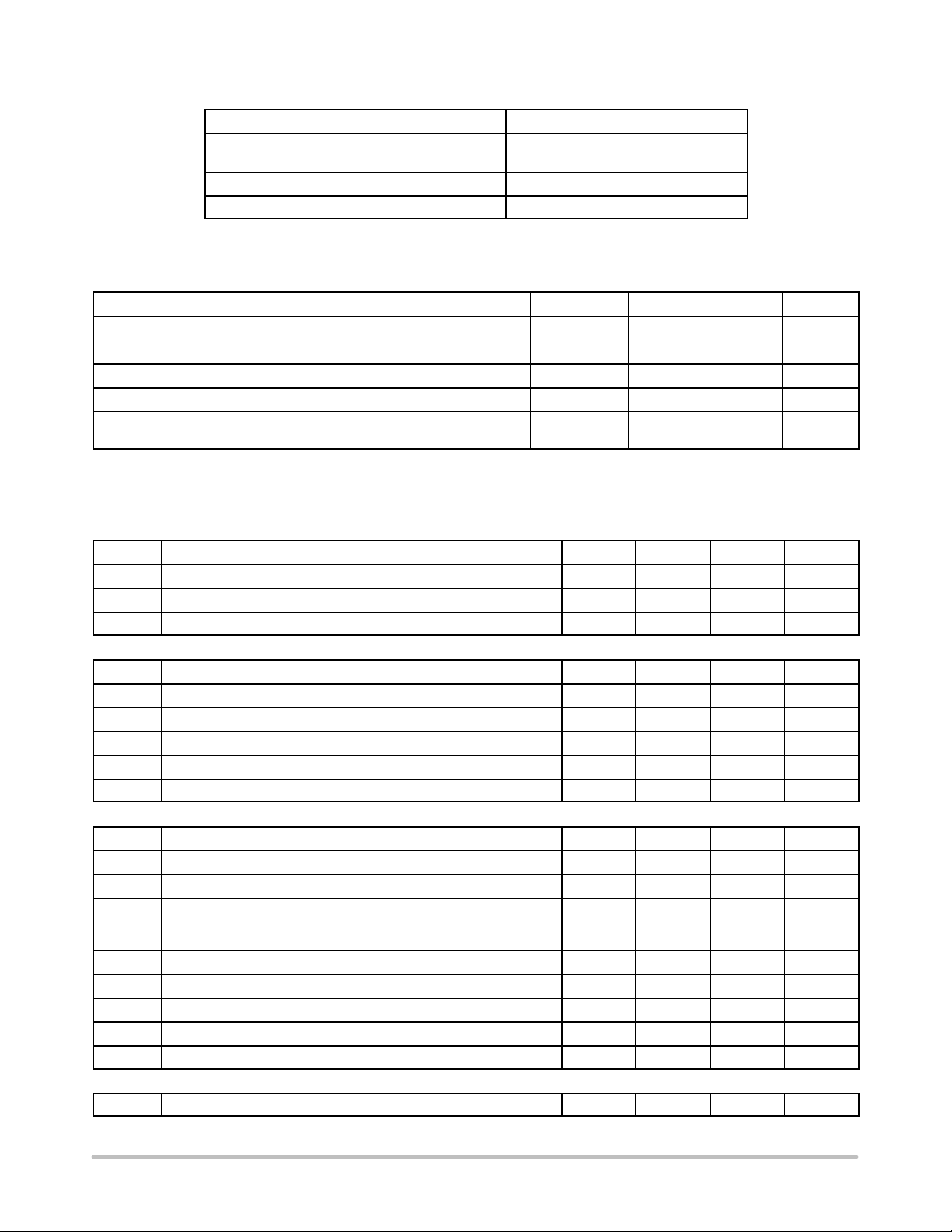
Table 1. ATTRIBUTES
Characteristics Value
ESD Human Body Model
Machine Model
Moisture Sensitivity (Note 1) Level 3
Flammability Rating Oxygen Index: 28 to 34 UL 94 V-0 @ 0.125 in.
1. For additional information, see Application Note AND8003/D
Table 2. MAXIMUM RATINGS
Parameter Symbol Rating Unit
Power Supply Voltage V
Output Driver Power Supply V
Operating Temperature Range T
Storage Temperature Range T
Thermal Resistance, Junction-to-Air
SO-20
Stresses exceeding Maximum Ratings may damage the device. Maximum Ratings are stress ratings only. Functional operation above the
Recommended Operating Conditions is not implied. Extended exposure to stresses above the Recommended Operating Conditions may affect
device reliability.
CC
CCO
stg
JA
2 kV
200 V
6 V
6 V
A
0 to +70 °C
-60 to +150 °C
°C/W
30 to 35
Table 3. DC & AC Characteristics (T
= 25°C, VCC = 5 V, RL = 150 , CL = 3 pF)
A
Symbol Parameter Min Typ Max Unit
V
V
I
CC
CCO
CC
Supply Voltage 4.75 5.0 5.25 V
Output Driver Power Supply 4.75 5.0 5.25 V
Power Supply Current (No Load) 20 30 40 mA
INPUTS
Signal Amplitude (CVBS signal) (Note 2) 1.0 V
Input Current (Per Output Connected) 1 3
DC Level (Bottom of Sync Pulse) 1.25 1.35 1.45 V
DC Level Shift (0°C to 70°C) (Note 2) 5 100 mV
R
IN
C
IN
Input Resistance (Note 2) 1
Input Capacitance (Note 2) 2 pF
OUTPUTS
Dynamic Range (VIN = 1 VPP) (Note 2) 1.9 2.0 2.1 V
Output Impedance (Note 2) 1
A
V
Gain (Note 2) 5.5 6.0 6.5 dB
BW Bandwidth (Note 2)
-1 dB Attenuation
-3 dB Attenuation
7 15
20
DG Differential Gain Error (Note 2) 0.5 %
DP Differential Phase Error (Note 2) 1.5 °
Crosstalk (f = 5 MHz) (Note 2) -65 -60 dB
DC Level (Bottom of Sync Pulse) 0.2 0.3 0.4 V
Continuous Output Current (Note 2) 20 mA
I2C BUS INPUT: DATA, CLOCK AND PROG
Threshold Voltage (Note 2) 1.5 2 3 V
2. Guaranteed by design and/or characterization.
PP
A
M
PP
MHz
http://onsemi.com
3
 Loading...