

Motorola MTW33N10E Datasheet

1
MOTOROLA
1
MTW33N10E
1
1
MTW33N10E
MOTOROLA
'
!&" $ " ##$!"
' &$ #!$ !% $ !
N-Channel Enhancement-Mode Silicon Gate
This advanced TMOS E-FET is designed to withstand high
energy in the avalanche and commutation modes. The new energy
efficient design also offers a drain-to-source diode with a fast
recovery time. Designed for low voltage, high speed switching
applications in p ower supplies, converters and P WM motor
controls, these devices are particularly well suited for bridge circuits
where diode speed and commutating safe operating areas are
critical and offer additional safety margin against unexpected
voltage transients.
• Avalanche Energy Specified
• Source-to-Drain Diode Recovery Time Comparable to a
Discrete Fast Recovery Diode
• Diode is Characterized for Use in Bridge Circuits
• I
DSS
and V
DS(on)
Specified at Elevated Temperature
• Isolated Mounting Hole Reduces Mounting Hardware
MAXIMUM RATINGS
(TJ = 25°C unless otherwise noted)
Rating
Symbol Value Unit
Drain-Source Voltage V
DSS
100 Vdc
Drain-Gate Voltage (RGS = 1.0 MΩ) V
DGR
100 Vdc
Gate-Source Voltage — Continuous
Gate-Source Voltage — Non-Repetitive (tp ≤ 10 ms)
V
GS
V
GSM
± 20
± 40
Vdc
Vpk
Drain Current — Continuous @ 25°C
— Continuous @ 100°C
— Single Pulse (tp ≤ 10 µs)
I
D
I
D
I
DM
33
20
99
Adc
Apk
Total Power Dissipation @ TC = 25°C
Derate above 25°C
P
D
125
1.0
Watts
W/°C
Operating and Storage Temperature Range TJ, T
stg
–55 to 150 °C
Single Pulse Drain-to-Source Avalanche Energy — Starting TJ = 25°C
(VDD = 25 Vdc, VGS = 10 Vdc, IL = 33 Apk, L = 1.000 mH, RG = 25 Ω)
E
AS
545 mJ
Thermal Resistance — Junction to Case
— Junction to Ambient
R
θJC
R
θJA
1.0
40
°C/W
Maximum Lead Temperature for Soldering Purposes, 1/8″ from case for 5 seconds T
L
260 °C
Designer’s Data for “Worst Case” Conditions — The Designer’s Data Sheet permits the design of most circuits entirely from the information presented. SOA Limit
curves — representing boundaries on device characteristics — are given to facilitate “worst case” design.
E-FET and Designer’s are trademarks of Motorola, Inc. TMOS is a registered trademark of Motorola, Inc.
Preferred devices are Motorola recommended choices for future use and best overall value.
Order this document
by MTW33N10E/D
SEMICONDUCTOR TECHNICAL DATA
Motorola, Inc. 1994
3/94
TMOS POWER FET
33 AMPERES
100 VOLTS
R
DS(on)
= 0.06 OHM
CASE 340F, Style 1
TO-247AE
Motorola Preferred Device
D
S
G
N-Channel
2
2
2
MOTOROLA
MTW33N10E
2
MTW33N10EMOTOROLA
ELECTRICAL CHARACTERISTICS (TC = 25°C unless otherwise noted)
Characteristic Symbol Min Typ Max Unit
OFF CHARACTERISTICS
Gate Threshold Voltage
(VDS = VGS, ID = 250 µAdc)
Temperature Coefficient (Negative)
V
GS(th)
2.0
—
—
7.0
4.0
—
Vdc
mV/°C
Static Drain-Source On-Resistance (VGS = 10 Vdc, ID = 16.5 Adc) R
DS(on)
— 0.04 0.06 Ohm
Drain-Source Breakdown Voltage
(VGS = 0 Vdc, ID = 250 µAdc)
Temperature Coefficient (Positive)
V
(BR)DSS
100
—
—
118
—
—
Vdc
mV/°C
Zero Gate Voltage Drain Current
(VDS = 100 Vdc, VGS = 0 Vdc)
(VDS = 100 Vdc, VGS = 0 Vdc, TJ = – 25°C)
I
DSS
—
—
—
—
10
100
µAdc
Gate-Body Leakage Current (VGS = ± 20 Vdc, VDS = 0) I
GSS
— — 100 nAdc
ON CHARACTERISTICS (1)
Drain-Source On-Voltage (VGS = 10 Vdc)
(ID = 33 Adc)
(ID = 16.5 Adc, TJ = – 25°C)
V
DS(on)
—
—
1.6
—
2.4
2.1
Vdc
Forward Transconductance (VDS = 8.0 Vdc, ID = 16.5 Adc) g
FS
8.0 — — mhos
DYNAMIC CHARACTERISTICS
Input Capacitance
C
iss
— 1830 2500 pF
Output Capacitance
(VDS = 25 Vdc, VGS = 0 Vdc,
C
oss
— 678 1200
Reverse Transfer Capacitance
f = 1.0 MHz)
C
rss
— 559 1100
SWITCHING CHARACTERISTICS (2)
Turn-On Delay Time
t
d(on)
— 18 40 ns
Rise Time
t
r
— 164 330
Turn-Off Delay Time
VGS = 10 Vdc,
RG = 9.1 Ω)
t
d(off)
— 48 100
Fall Time
RG = 9.1 Ω)
t
f
— 83 170
Q
T
— 52 110 nC
(See Figure 8)
DS
= 80 Vdc, ID = 33 Adc,
Q
1
— 12 —
(VDS = 80 Vdc, ID = 33 Adc,
VGS = 10 Vdc)
Q
2
— 32 —
Q
3
— 24 —
SOURCE-DRAIN DIODE CHARACTERISTICS
Forward On-Voltage (1)
(IS = 33 Adc, VGS = 0 Vdc)
(IS = 33 Adc, VGS = 0 Vdc, TJ = 125°C)
V
SD
—
—
1.0
0.98
2.0
—
Vdc
t
rr
— 144 —
(See Figure 14)
S
= 33 Adc, VGS = 0 Vdc,
t
a
— 108 —
(IS = 33 Adc, VGS = 0 Vdc,
dIS/dt = 100 A/µs)
t
b
— 36 —
Reverse Recovery Stored Charge Q
RR
— 0.93 — µC
INTERNAL PACKAGE INDUCTANCE
Internal Drain Inductance
(Measured from the drain lead 0.25″ from package to center of die)
L
D
— 4.5 — nH
Internal Source Inductance
(Measured from the source lead 0.25″ from package to source bond pad)
L
S
— 13 — nH
(1) Pulse Test: Pulse Width ≤ 300 µs, Duty Cycle ≤ 2%.
(2) Switching characteristics are independent of operating junction temperature.
Gate Charge
Reverse Recovery Time
(VDD = 50 Vdc, ID = 33 Adc,
(V
(I
ns
3
MOTOROLA
3
MTW33N10E
3
3
MTW33N10E
MOTOROLA
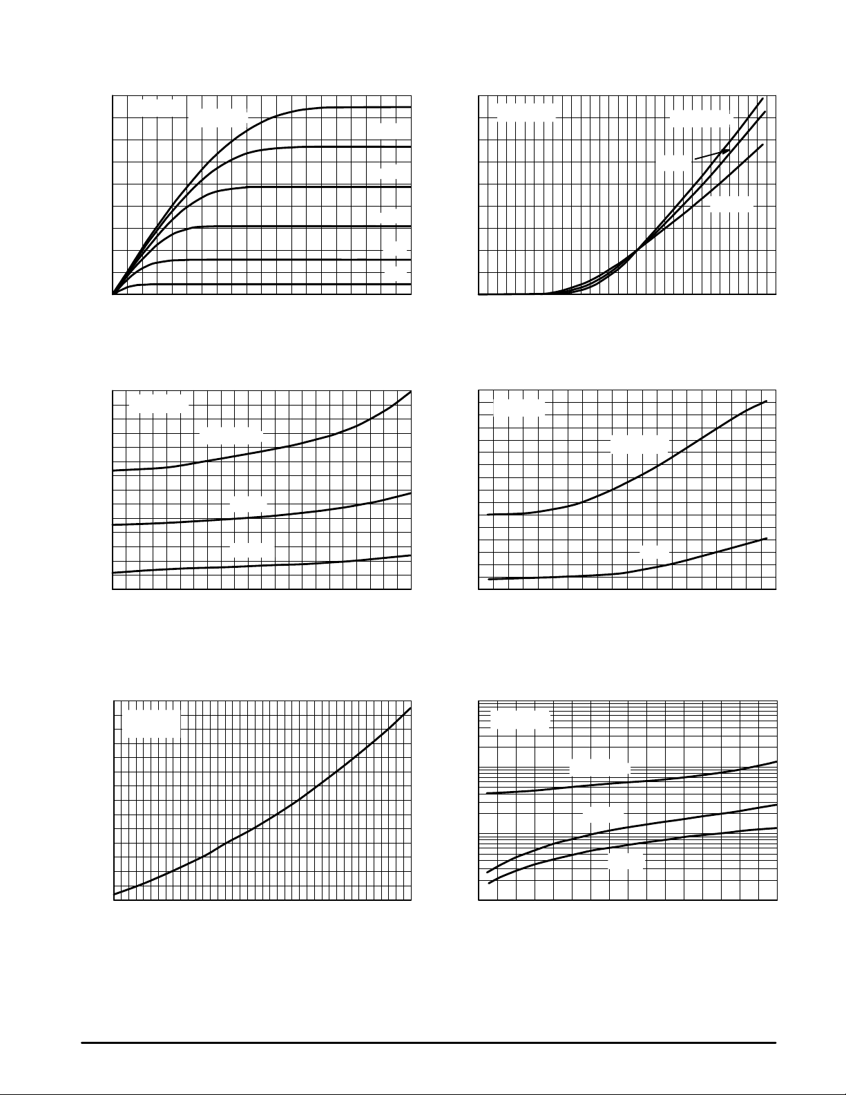
TYPICAL ELECTRICAL CHARACTERISTICS
5 11 23 35 53 65
0.037
0.039
0.045
0.053
0.051
0.049
0.043
17 29 41 47 59
0.047
0 18 42 54 60 66
0.02
0.03
0.06
0.07
0.09
0.04
0.05
30 36 48
6
0.08
2.0
0
30
50
80
90
70
40
20
2.5 3.0 3.5 5.5 6.0 6.5 7.0 7.5 8.0 10
60
4.0 4.5 5.01 3 5 7 9
70
90
2 4 6 10
20
50
0
0
VDS, DRAIN-TO-SOURCE VOLTAGE (VOLTS)
Figure 1. On-Region Characteristics
I
D
, DRAIN CURRENT (AMPS)
I
D
, DRAIN CURRENT (AMPS)
VGS, GATE-TO-SOURCE VOLTAGE (VOLTS)
Figure 2. Transfer Characteristics
R
DS(on)
, DRAIN-TO-SOURCE RESISTANCE (OHMS)
ID, DRAIN CURRENT (AMPS)
Figure 3. On-Resistance versus Drain Current
and Temperature
ID, DRAIN CURRENT (AMPS)
Figure 4. On-Resistance versus Drain Current
and Gate Voltage
R
DS(on)
TJ, JUNCTION TEMPERATURE (°C)
Figure 5. On-Resistance Variation with
Temperature
VDS, DRAIN-TO-SOURCE VOLTAGE (VOLTS)
Figure 6. Drain-To-Source Leakage
Current versus Voltage
R
DS(on)
, DRAIN-TO-SOURCE RESISTANCE (OHMS)
, DRAIN-TO-SOURCE RESISTANCE
(NORMALIZED)
I
DSS
, LEAKAGE (nA)
TJ = 25
°C
TJ = – 55
°C
25
°C
100
°C
TJ = 100
°C
25
°C
–55
°C
VGS = 10 V
VGS = 10 V
9 V
5 V
6 V
7 V
8 V
20 100
10
1000
10000
6040 80–50
0.6
1.6
2.0
–25 0 25 50 75 100 125 150
0.8
1.2
1.8
VGS = 10 V
15 V
TJ = 25
°C
VGS = 10 V
ID = 16.5 A
TJ = 125
°C
25
°C
100
°C
VGS = 0 V
100
30
80
60
40
10
8
VDS ≥ 10 V
10
8.5 9.0 9.5
12 24
1.0
1.4
5030 70 90
0.041
 Loading...