

Motorola MTP75N03HDL Datasheet
1
Motorola TMOS Power MOSFET Transistor Device Data
N–Channel Enhancement–Mode Silicon Gate
This advanced high–cell density HDTMOS E–FET is designed to
withstand high energy in the avalanche and commutation modes.
This new energy efficient design also o ffers a drain–to–source
diode w ith a f ast r ecovery t ime. Designed for l ow–voltage,
high–speed switching applications in power supplies, converters
and PWM m otor controls, a nd inductive loads. The a valanche
energy capability is specified to eliminate the guesswork in designs
where inductive loads are switched, and to offer additional safety
margin against unexpected voltage transients.
• Ultra Low R
DS(on)
, High–Cell Density, HDTMOS
• SPICE Parameters Available
• Diode is Characterized for Use in Bridge Circuits
• I
DSS
and V
DS(on)
Specified at Elevated Temperature
• Avalanche Energy Specified
MAXIMUM RATINGS
(TC = 25°C unless otherwise noted)
Rating Symbol Value Unit
Drain–Source Voltage V
DSS
25 Vdc
Drain–Gate Voltage (RGS = 1.0 MΩ) V
DGR
25 Vdc
Gate–Source Voltage — Continuous
Gate–Source Voltage — Single Pulse (tp ≤ 10 ms)
V
GS
± 15
± 20
Vdc
Vpk
Drain Current — Continuous
— Continuous @ 100°C
— Single Pulse (tp ≤ 10 µs)
I
D
I
D
I
DM
75
59
225
Adc
Apk
Total Power Dissipation
Derate above 25°C
P
D
150
1.0
Watts
W/°C
Operating and Storage Temperature Range TJ, T
stg
–55 to 175 °C
Single Pulse Drain–to–Source Avalanche Energy — Starting TJ = 25°C
(VDD = 25 Vdc, VGS = 5.0 Vdc, IL = 75 Apk, L = 0.1 mH, RG = 25 Ω)
E
AS
280 mJ
Thermal Resistance — Junction to Case
— Junction to Ambient
R
θJC
R
θJA
1.0
62.5
°C/W
Maximum Lead Temperature for Soldering Purposes, 1/8″ from case for 10 seconds T
L
260 °C
This document contains information on a new product. Specifications and information herein are subject to change without notice.
E–FET and HDTMOS are trademarks of Motorola, Inc.
TMOS is a registered trademark of Motorola, Inc.
Preferred devices are Motorola recommended choices for future use and best overall value.
REV 2
Order this document
by MTP75N03HDL/D
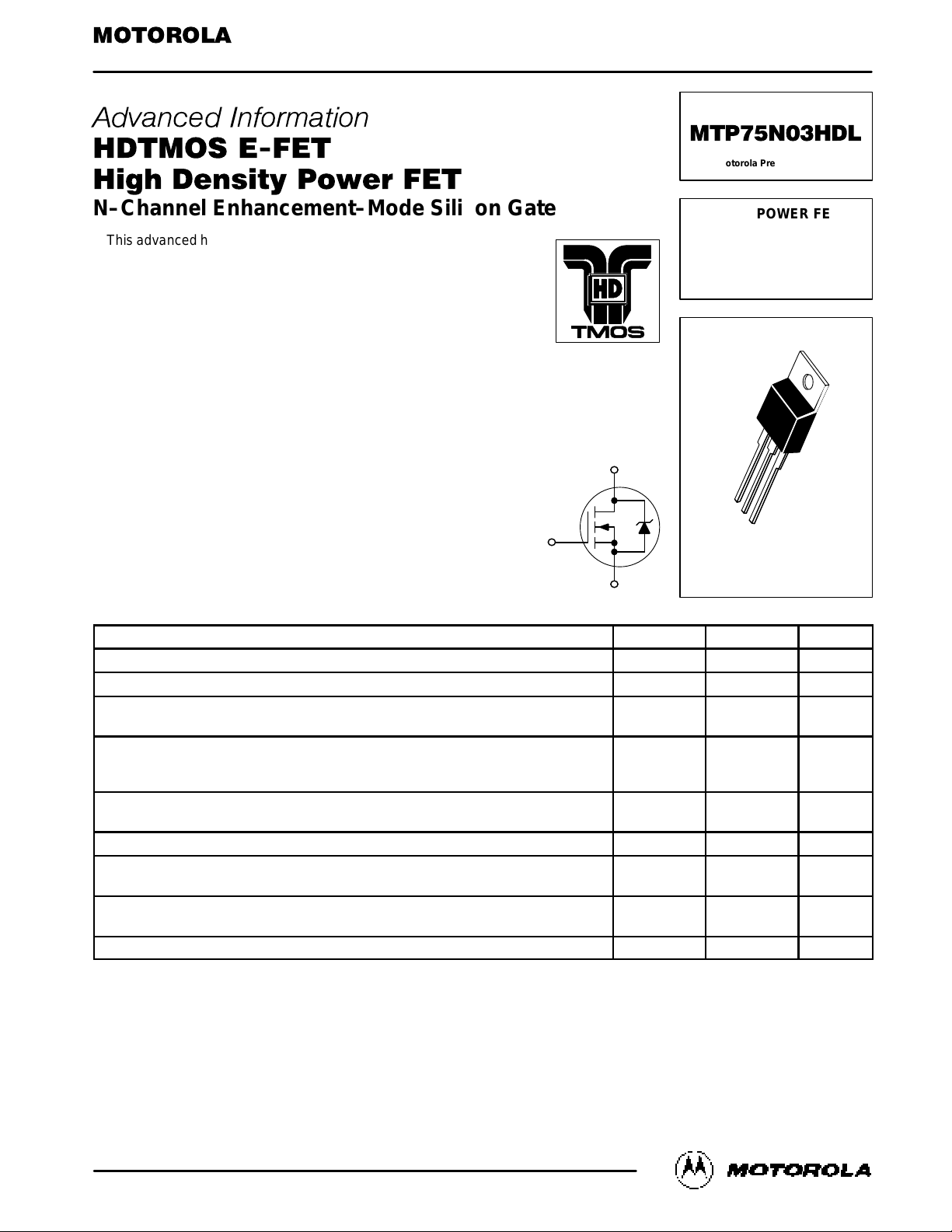
SEMICONDUCTOR TECHNICAL DATA
Motorola, Inc. 1995
TMOS POWER FET
LOGIC LEVEL
75 AMPERES
R
DS(on)
= 9.0 mOHM
25 VOLTS
Motorola Preferred Device
D
S
G
CASE 221A–06, Style 5
TO–220AB
MTP75N03HDL
2
Motorola TMOS Power MOSFET Transistor Device Data
ELECTRICAL CHARACTERISTICS
(TJ = 25°C unless otherwise noted)
Characteristic
Symbol Min Typ Max Unit
OFF CHARACTERISTICS
Drain–Source Breakdown Voltage
(Cpk ≥ 2.0) (3)
(VGS = 0 Vdc, ID = 0.25 mA)
Temperature Coefficient (Positive)
V
(BR)DSS
25 — —
Vdc
mV/°C
Zero Gate Voltage Drain Current
(VDS = 25 Vdc, VGS = 0 Vdc)
(VDS = 25 Vdc, VGS = 0 Vdc, TJ = 125°C)
I
DSS
—
—
—
—
100
500
µAdc
Gate–Body Leakage Current (VGS = ± 20 Vdc, VDS = 0 V) I
GSS
— — 100 nAdc
ON CHARACTERISTICS (1)
Gate Threshold Voltage (Cpk ≥ 3.0) (3)
(VDS = VGS, ID = 0.25 mA)
Temperature Coefficient (Negative)
V
GS(th)
1.0 1.5 2.0
Vdc
mV/°C
Static Drain–Source On–Resistance
(Cpk ≥ 2.0) (3)
(VGS = 5.0 Vdc, ID = 37.5 Adc)
R
DS(on)
— 6.0 9.0
mΩ
Drain–Source On–Voltage (VGS = 10 Vdc)
(ID = 75 Adc)
(ID = 37.5 Adc, TJ = 125°C)
V
DS(on)
—
—
—
0.68
0.6
Vdc
Forward Transconductance (VDS = 3.0 Vdc, ID = 20 Adc) g
FS
15 55 — mhos
DYNAMIC CHARACTERISTICS
Input Capacitance
C
iss
— 4025 5635 pF
Output Capacitance
(VDS = 25 Vdc, VGS = 0 Vdc,
f = 1.0 MHz)
C
oss
— 1353 1894
Reverse Transfer Capacitance
f = 1.0 MHz)
C
rss
— 307 430
SWITCHING CHARACTERISTICS (2)
Turn–On Delay Time
t
d(on)
— 24 48 ns
Rise Time
t
r
— 493 986
Turn–Off Delay Time
VGS = 5.0 Vdc,
Rg = 4.7 Ω)
t
d(off)
— 60 120
Fall Time
g
= 4.7 Ω)
t
f
— 149 300
Q
T
— 61 122 nC
DS
= 24 Vdc, ID = 75 Adc,
Q
1
— 14 28
(VDS = 24 Vdc, ID = 75 Adc,
VGS = 5.0 Vdc)
Q
2
— 33 66
Q
3
— 27 54
SOURCE–DRAIN DIODE CHARACTERISTICS
Forward On–Voltage
(IS = 75 Adc, VGS = 0 Vdc)
(IS = 75 Adc, VGS = 0 Vdc, TJ = 125°C)
V
SD
—
—
0.97
0.87
1.1
—
Vdc
t
rr
— 58 —
S
= 75 Adc, VGS = 0 Vdc,
t
a
— 27 —
(IS = 75 Adc, VGS = 0 Vdc,
dIS/dt = 100 A/µs)
t
b
— 30 —
Reverse Recovery Stored Charge Q
RR
— 0.088 — µC
(1) Pulse Test: Pulse Width ≤ 300 µs, Duty Cycle ≤ 2%.
(2) Switching characteristics are independent of operating junction temperature.
(3) Reflects typical values.
Cpk =
Max limit – Typ
3 x SIGMA
Gate Charge
Reverse Recovery Time
(VDS = 15 Vdc, ID = 75 Adc,
(V
(I
ns
MTP75N03HDL
3
Motorola TMOS Power MOSFET Transistor Device Data
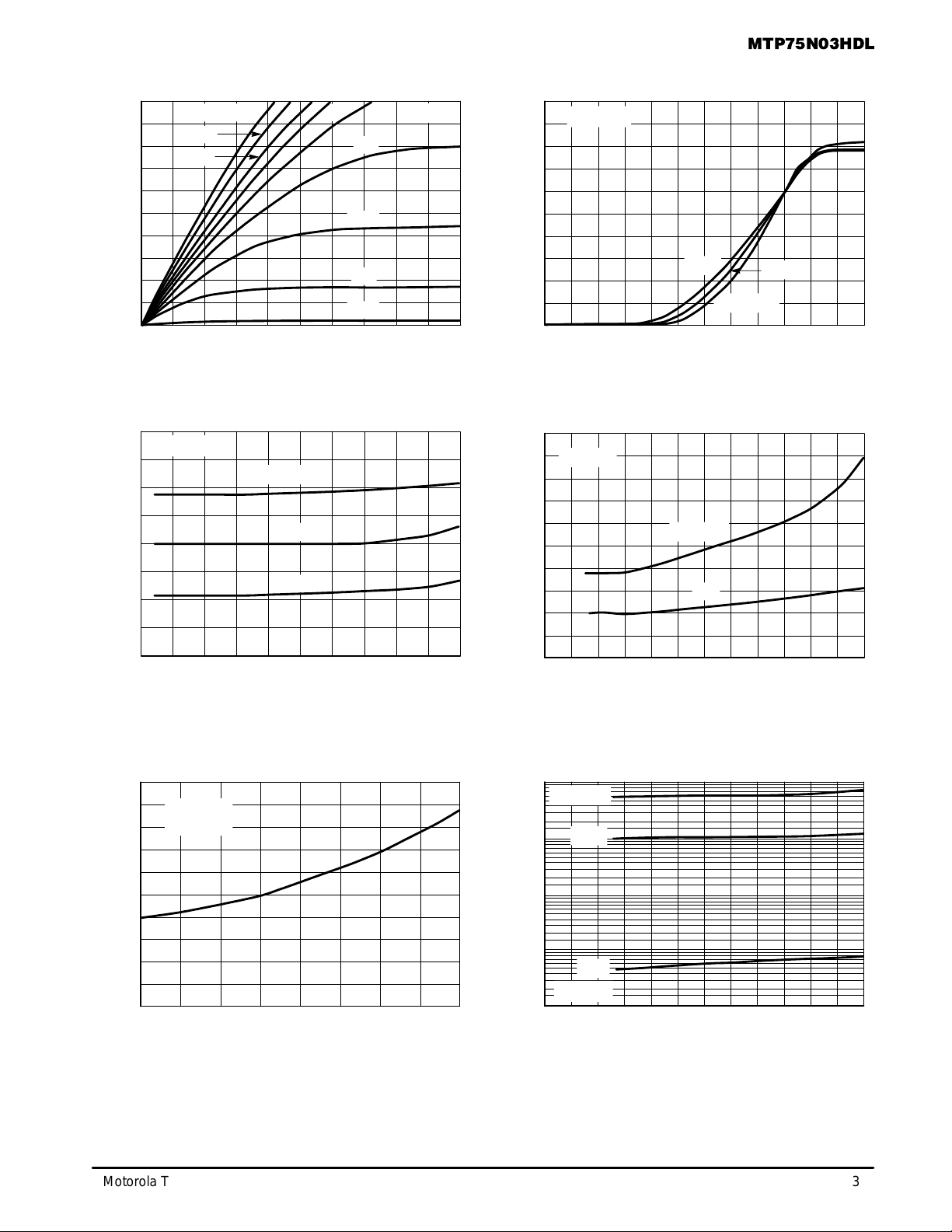
TYPICAL ELECTRICAL CHARACTERISTICS
R
DS(on)
, DRAIN–TO–SOURCE RESISTANCE (OHMS)
R
DS(on)
, DRAIN–TO–SOURCE RESISTANCE
(NORMALIZED)
VDS, DRAIN–TO–SOURCE VOLTAGE (VOLTS)
Figure 1. On–Region Characteristics
I
D
, DRAIN CURRENT (AMPS)
I
D
, DRAIN CURRENT (AMPS)
VGS, GATE–TO–SOURCE VOLTAGE (VOLTS)
Figure 2. Transfer Characteristics
R
DS(on)
, DRAIN–TO–SOURCE RESISTANCE (OHMS)
ID, DRAIN CURRENT (AMPS)
Figure 3. On–Resistance versus Drain Current
and Temperature
ID, DRAIN CURRENT (AMPS)
Figure 4. On–Resistance versus Drain Current
and Gate Voltage
TJ, JUNCTION TEMPERATURE (°C)
Figure 5. On–Resistance Variation with
Temperature
VDS, DRAIN–TO–SOURCE VOLTAGE (VOLTS)
Figure 6. Drain–To–Source Leakage
Current versus Voltage
I
DSS
, LEAKAGE (nA)
TJ = 25
°C
VDS ≥ 10 V
TJ = 100
°C
25
°C
–55
°C
TJ = 25
°C
VGS = 0 V
VGS = 10 V
VGS = 5 V
VGS = 5 V
VGS = 10 V
ID = 37.5 A
0.4 0.8 1.2 1.6 20 0.2 0.6 1 1.4 1.8
30
60
90
120
150
0
2 2.5 3.5 4 4.51.5
30
60
90
120
150
0
3
30 60 90 120 1500
0.01
0.002
0.008
0.006
0.004
25 50 100 125 1500
0.005
0.006
0.007
0.008
0.009
0.004
75
25 100 150–50 –25 0 50 75 125
0.4
0.8
1.2
1.6
2
0
10 20 300 5 15 25
10
100
1000
10000
1
10 V
100°C
25°C
TJ = 125°C
100°C
25°C
TJ = –55
°C
3.5 V
3 V
4 V
2.5 V
4.5 V
5 V
8 V
6 V
 Loading...