


SEMICONDUCTOR TECHNICAL DATA
N–Channel Enhancement–Mode Silicon Gate
This advanced high voltage TMOS E–FET is designed to
withstand high energy in the avalanche mode and switch efficiently .
This new high energy device also offers a drain–to–source diode
with fast recovery time. Designed for high voltage, high speed
switching applications such as power supplies, PWM motor
controls and other inductive loads, the avalanche energy capability
is specified to eliminate the guesswork in designs where inductive
loads are switched and offer additional safety margin against
unexpected voltage transients.
• Avalanche Energy Capability Specified at Elevated
Temperature
• Low Stored Gate Charge for Efficient Switching
• Internal Source–to–Drain Diode Designed to Replace External
Zener Transient Suppressor — Absorbs High Energy in the
Avalanche Mode
• Source–to–Drain Diode Recovery Time Comparable to Discrete
Fast Recovery Diode
G
Order this document
by MTP3N60E/D
Motorola Preferred Device
TMOS POWER FET
3.0 AMPERES
600 VOL TS
R
D
S
DS(on)
= 2.2 OHMS
CASE 221A–09, Style 5
TO-220AB
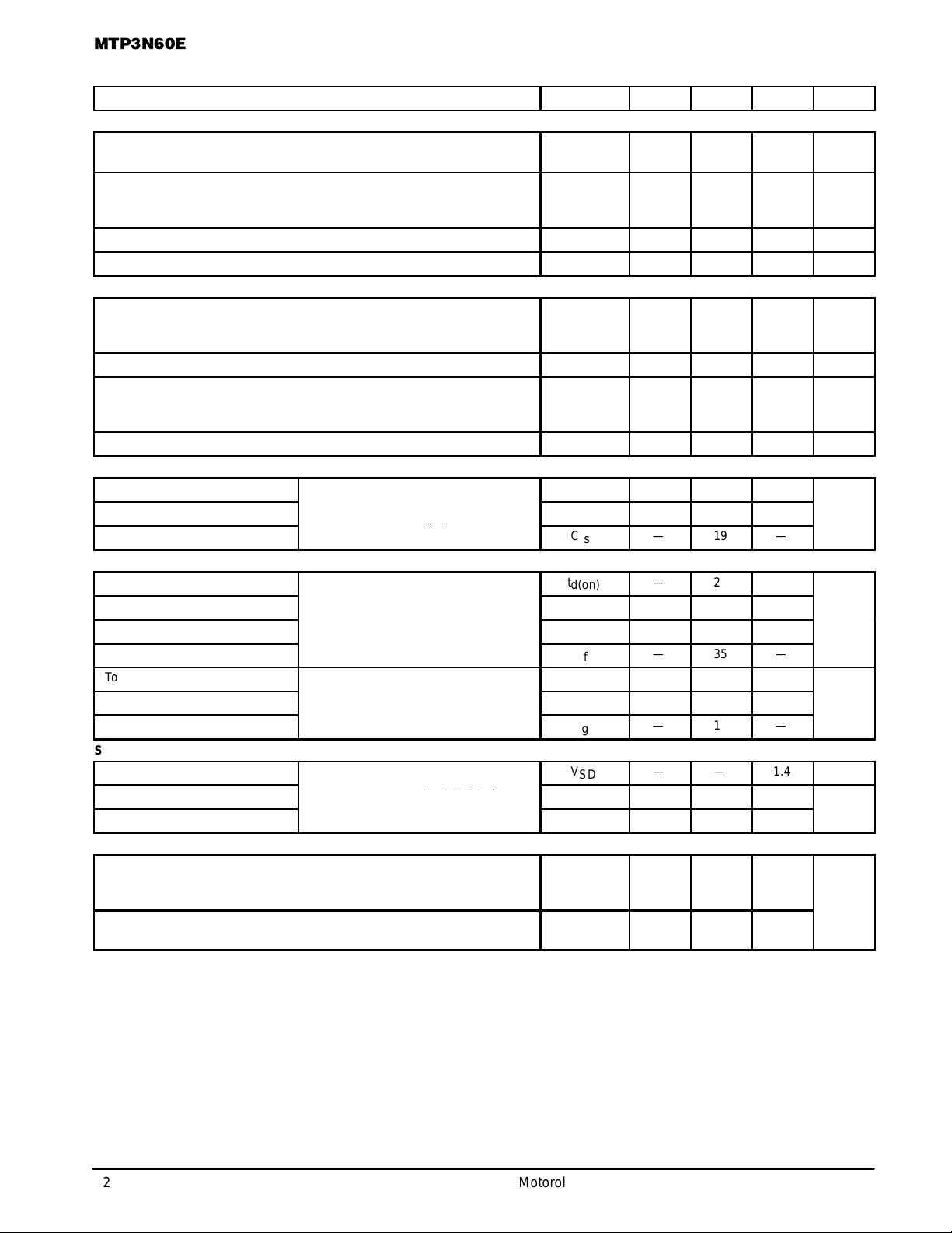
MAXIMUM RATINGS
Drain–Source Voltage V
Drain–Gate Voltage (RGS = 1.0 MΩ) V
Gate–Source Voltage — Continuous
Gate–Source Voltage — Non–repetitive
Drain Current — Continuous
Drain Current — Continuous @ 100°C
Drain Current — Pulsed
Total Power Dissipation @ TC = 25°C
Derate above 25°C
Operating and Storage Temperature Range TJ, T
UNCLAMPED DRAIN–TO–SOURCE AVALANCHE CHARACTERISTICS (T
Single Pulse Drain–to–Source Avalanche Energy — TJ = 25°C
Single Pulse Drain–to–Source Avalanche Energy — TJ = 100°C
Repetitive Pulse Drain–to–Source Avalanche Energy
(TC = 25°C unless otherwise noted)
Rating Symbol Value Unit
< 150°C)
J
V
V
I
W
DSR(1)
W
DSR(2)
DSS
DGR
GS
GSM
I
D
I
D
DM
P
D
stg
600 Vdc
600 Vdc
±20
±40
3.0
2.4
14
75
0.6
–55 to 150 °C
290
46
7.5
Vdc
Vpk
Adc
Watts
W/°C
mJ
THERMAL CHARACTERISTICS
Thermal Resistance — Junction to Case°
Thermal Resistance — Junction to Ambient°
Maximum Lead Temperature for Soldering Purposes, 1/8″ from case for 10 seconds T
(1) VDD = 50 V, ID = 3.0 A
(2) Pulse Width and frequency is limited by TJ(max) and thermal response
Designer’s Data for “Worst Case” Conditions — The Designer’s Data Sheet permits the design of most circuits entirely from the information presented. SOA Limit
curves —representing boundaries on device characteristics — are given to facilitate “worst case” design.
E–FET and Designer’s are trademarks of Motorola, Inc. TMOS is a registered trademark of Motorola, Inc.
Preferred devices are Motorola recommended choices for future use and best overall value.
REV 2
R
R
θJC
θJA
L
1.67
62.5
260 °C
°C/W
Motorola TMOS Power MOSFET Transistor Device Data
Motorola, Inc. 1997
1
MTP3N60E
)
f = 1.0 MHz)
R
100 Ω, R
12 Ω
GS(on)
)
)
V
GS
V)
ELECTRICAL CHARACTERISTICS
OFF CHARACTERISTICS
Drain–to–Source Breakdown Voltage
(VGS = 0, ID = 250 µAdc)
Zero Gate Voltage Drain Current
(VDS = 600 V, VGS = 0)
(VDS = 480 V, VGS = 0, TJ = 125°C)
Gate–Body Leakage Current — Forward (V
Gate–Body Leakage Current — Reverse (V
ON CHARACTERISTICS*
Gate Threshold Voltage
(VDS = VGS, ID = 250 µAdc)
(TJ = 125°C)
Static Drain–to–Source On–Resistance (VGS = 10 Vdc, ID = 1.5 A) R
Drain–to–Source On–Voltage (VGS = 10 Vdc)
(ID = 3.0 A)
(ID = 1.5 A, TJ = 100°C)
Forward Transconductance (VDS = 15 Vdc, ID = 1.5 A) g
DYNAMIC CHARACTERISTICS
Input Capacitance
Output Capacitance
Transfer Capacitance
SWITCHING CHARACTERISTICS*
Turn–On Delay Time
Rise Time
Turn–Off Delay Time
Fall Time
Total Gate Charge
Gate–Source Charge
Gate–Drain Charge
SOURCE–DRAIN DIODE CHARACTERISTICS
Forward On–Voltage
Forward Turn–On Time
Reverse Recovery Time t
INTERNAL PACKAGE INDUCTANCE
Internal Drain Inductance
(Measured from the contact screw on tab to center of die)
(Measured from the drain lead 0.25″ from package to center of die)
Internal Source Inductance
(Measured from the source lead 0.25″ from package to source bond pad)
*Pulse T est: Pulse Width = 300 µ s, Duty Cycle ≤ 2.0%.
**Limited by circuit inductance.
(T
= 25°C unless otherwise noted)
J
Characteristic
GSF
GSR
(IS = 3.0 A, di/dt = 100 A/µs)
= 20 Vdc, VDS = 0) I
= 20 Vdc, VDS = 0) I
(VDS = 25 V, VGS = 0,
f = 1.0 MHz
(VDD = 300 V, ID ≈ 3.0 A,
=
L
V
GS(on)
(VDS = 420 V, ID = 3.0 A,
V
G
= 10 V)
= 10 V
= 10
=
,
Symbol Min Typ Max Unit
V
(BR)DSS
I
DSS
GSSF
GSSR
V
GS(th)
DS(on)
V
DS(on)
FS
C
iss
C
oss
C
rss
t
d(on)
t
r
t
d(off)
t
f
Q
g
Q
gs
Q
gd
V
SD
t
on
rr
L
d
L
s
600 — — Vdc
—
—
— — 100 nAdc
— — 100 nAdc
2.0
1.5
— 2.1 2.2 Ohms
—
—
1.5 — — mhos
— 770 — pF
— 105 —
— 19 —
— 23 — ns
— 34 —
— 58 —
— 35 —
— 28 31 nC
— 5.0 —
— 17 —
— — 1.4 Vdc
— ** —
— 400 —
—
—
— 7.5 —
—
—
—
—
—
—
3.5
4.5
10
100
4.0
3.5
9.0
7.5
—
—
µAdc
Vdc
Vdc
ns
nH
2
Motorola TMOS Power MOSFET Transistor Device Data
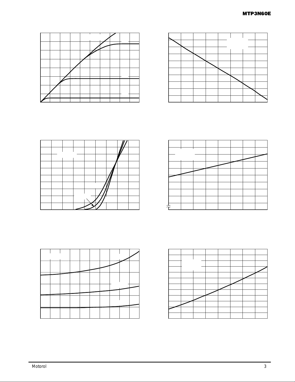
TYPICAL ELECTRICAL CHARACTERISTICS
D
MTP3N60E
8
6
4
, DRAIN CURRENT (AMPS)
2
D
I
0
10
8
6
VGS = 10 V
7 V
6 V
5 V
2 6 10 14 18
VDS, DRAIN–TO–SOURCE VOL TAGE (VOLTS)
Figure 1. On–Region Characteristics
VDS ≥ 10 V
1.2
VDS = V
GS
1.1
1
0.9
0.8
, GATE THRESHOLD VOLTAGE (NORMALIZE
201612840
0.7
–50 –25 0 25 50 75 100 125 150
GS(th)
V
TJ, JUNCTION TEMPERATURE (°C)
ID = 0.25 mA
Figure 2. Gate–Threshold V oltage Variation
With Temperature
1.2
VGS = 0
1.1
ID = 250
µ
A
1
4
, DRAIN CURRENT (AMPS)
D
I
2
0
6
4
2
, DRAIN–TO–SOURCE RESIST ANCE (OHMS)
0
DS(on)
R
0.9
100°C
TJ = 25°C
1 3 5 7 9 –25 25 75 125
VGS, GATE–T O–SOURCE VOLTAGE (VOLTS)
–55°C
86420
Figure 3. Transfer Characteristics
(NORMALIZED)
0.8
, DRAIN–TO–SOURCE BREAKDOWN VOL TAGE
–50 0 50 100 150
BR(DSS)
V
TJ, JUNCTION TEMPERATURE (°C)
Figure 4. Breakdown V oltage Variation
With Temperature
3
VGS = 10 V
ID, DRAIN CURRENT (AMPS)
100°C
TJ = 25°C
–55°C
8
VGS = 10 V
ID = 2 A
2
1
(NORMALIZED)
, DRAIN–TO–SOURCE ON–RESISTANCE
DS(on)
0
R
106420
–50 0 50 100 150–25 25 75 125
TJ, JUNCTION TEMPERATURE (°C)
Figure 5. On–Resistance versus Drain Current
Motorola TMOS Power MOSFET Transistor Device Data
Figure 6. On–Resistance Variation
With Temperature
3
 Loading...