

MOTOROLA MTD3055VL, MTD3055VL1, MTD3055VLT4 Datasheet
MTD3055VL
Preferred Device
Power MOSFET
12 Amps, 60 Volts
N–Channel DPAK
This Power MOSFET is designed to withstand high energy in the
avalanche and commutation modes. Designed for low voltage, high
speed switching applications in power supplies, converters and power
motor controls, these devices are particularly well suited for bridge
circuits where diode speed and commutating safe operating areas are
critical and offer additional safety margin against unexpected voltage
transients.
• Avalanche Energy Specified
• I
and V
DSS
MAXIMUM RATINGS (T
Drain–Source Voltage V
Drain–Gate Voltage (RGS = 1.0 MΩ) V
Gate–Source Voltage
– Continuous
– Single Pulse (tp ≤ 50 ms)
Drain Current – Continuous @ 25°C
Drain Current – Continuous @ 100°C
Drain Current – Single Pulse (tp ≤ 10 µs)
Total Power Dissipation @ 25°C
Derate above 25°C
Total Power Dissipation @ TA = 25°C, when
mounted to minimum recommended pad
size
Operating and Storage Temperature
Range
Single Pulse Drain–to–Source Avalanche
Energy – Starting TJ = 25°C
(VDD = 25 Vdc, VGS = 5.0 Vdc,
IL = 12 Apk, L = 1.0 mH, RG = 25 Ω)
Thermal Resistance
– Junction to Case
– Junction to Ambient
– Junction to Ambient, when mounted to
minimum recommended pad size
Maximum Temperature for Soldering
Purposes, 1/8″ from case for 10
seconds
Specified at Elevated Temperature
DS(on)
= 25°C unless otherwise noted)
C
Rating
Symbol Value Unit
DSS
DGR
V
V
GSM
I
DM
P
TJ, T
E
R
R
R
T
GS
I
D
I
D
D
AS
θJC
θJA
θJA
L
stg
60 Vdc
60 Vdc
±15
± 20
12
8.0
42
48
0.32
1.75
–55 to
175
72 mJ
3.13
100
71.4
260 °C
Vdc
Vpk
Adc
Apk
Watts
W/°C
Watts
°C
°C/W
http://onsemi.com
12 AMPERES
60 VOLTS
R
DS(on)
N–Channel
D
G
4
CASE 369A
2
1
3
Y = Year
WW = Work Week
T = MOSFET
ORDERING INFORMATION
DPAK
STYLE 2
PIN ASSIGNMENT
Drain
1
Gate
Drain
= 180 mΩ
S
MARKING
DIAGRAM
4
3
2
Source
YWW
T
3055VL
Semiconductor Components Industries, LLC, 2000
November, 2000 – Rev. 3
Device Package Shipping
MTD3055VL DPAK 75 Units/Rail
MTD3055VL1 DPAK 75 Units/Rail
MTD3055VLT4 DPAK 2500 Tape & Reel
Preferred devices are recommended choices for future use
and best overall value.
1 Publication Order Number:
MTD3055VL/D
MTD3055VL
)
f = 1.0 MHz)
R
G
9.1 Ω)
(V
DS
Vdc, I
D
Adc
dIS/dt = 100 A/µs)
ELECTRICAL CHARACTERISTICS (T
Characteristic
OFF CHARACTERISTICS
Drain–Source Breakdown Voltage
(VGS = 0 Vdc, ID = 250 µAdc)
Temperature Coefficient (Positive)
Zero Gate Voltage Drain Current
(VDS = 60 Vdc, VGS = 0 Vdc)
(VDS = 60 Vdc, VGS = 0 Vdc, TJ = 150°C)
Gate–Body Leakage Current (VGS = ±15 Vdc, VDS = 0 Vdc) I
ON CHARACTERISTICS (Note 1.)
Gate Threshold Voltage
(VDS = VGS, ID = 250 µAdc)
Threshold Temperature Coefficient (Negative)
Static Drain–Source On–Resistance (VGS = 5.0 Vdc, ID = 6.0 Adc) R
Drain–Source On–Voltage (VGS = 5.0 Vdc)
(ID = 12 Adc)
(ID = 6.0 Adc, TJ = 150°C)
Forward Transconductance (VDS = 8.0 Vdc, ID = 6.0 Adc) g
DYNAMIC CHARACTERISTICS
Input Capacitance
Output Capacitance
Reverse Transfer Capacitance
SWITCHING CHARACTERISTICS (Note 2.)
Turn–On Delay Time
Rise Time
Turn–Off Delay Time
Fall Time
Gate Charge
(See Figure 8)
SOURCE–DRAIN DIODE CHARACTERISTICS
Forward On–Voltage (Note 1.)
(IS = 12 Adc, VGS = 0 Vdc, TJ = 150°C)
Reverse Recovery Time
(See Figure 14)
Reverse Recovery Stored
Charge
INTERNAL PACKAGE INDUCTANCE
Internal Drain Inductance
(Measured from the drain lead 0.25″ from package to center of die)
Internal Source Inductance
(Measured from the source lead 0.25″ from package to source bond pad)
1. Pulse Test: Pulse Width ≤300 µs, Duty Cycle ≤ 2%.
2. Switching characteristics are independent of operating junction temperature.
= 25°C unless otherwise noted)
J
(VDS = 25 Vdc, VGS = 0 Vdc,
f = 1.0 MHz
(VDD = 30 Vdc, ID = 12 Adc,
VGS = 5.0 Vdc,
RG = 9.1 Ω)
(VDS = 48 Vdc, ID = 12 Adc,
48
VGS = 5 Vdc)
(IS = 12 Adc, VGS = 0 Vdc)
(IS = 12 Adc, VGS = 0 Vdc,
dIS/dt = 100 A/µs)
12
,
Symbol Min Typ Max Unit
V
(BR)DSS
I
DSS
GSS
V
GS(th)
DS(on)
V
DS(on)
FS
C
iss
C
oss
C
rss
t
d(on)
t
r
t
d(off)
t
f
Q
T
Q
1
Q
2
Q
3
V
SD
t
rr
t
a
t
b
Q
RR
L
D
L
S
60
–
–
–
– – 100 nAdc
1.0
–
– 0.12 0.18 Ohm
–
–
5.0 8.8 – mhos
– 410 570 pF
– 114 160
– 21 40
– 9.0 20 ns
– 85 190
– 14 30
– 43 90
– 8.1 10 nC
– 1.8 –
– 4.2 –
– 3.8 –
–
–
– 55.7 –
– 37 –
– 18.7 –
– 0.116 – µC
– 3.5 – nH
– 7.5 – nH
–
62
–
–
1.6
3.0
1.6
–
0.97
0.86
–
–
10
100
2.0
–
2.6
2.5
1.3
–
mV/°C
mV/°C
Vdc
µAdc
Vdc
Vdc
Vdc
ns
http://onsemi.com
2
MTD3055VL
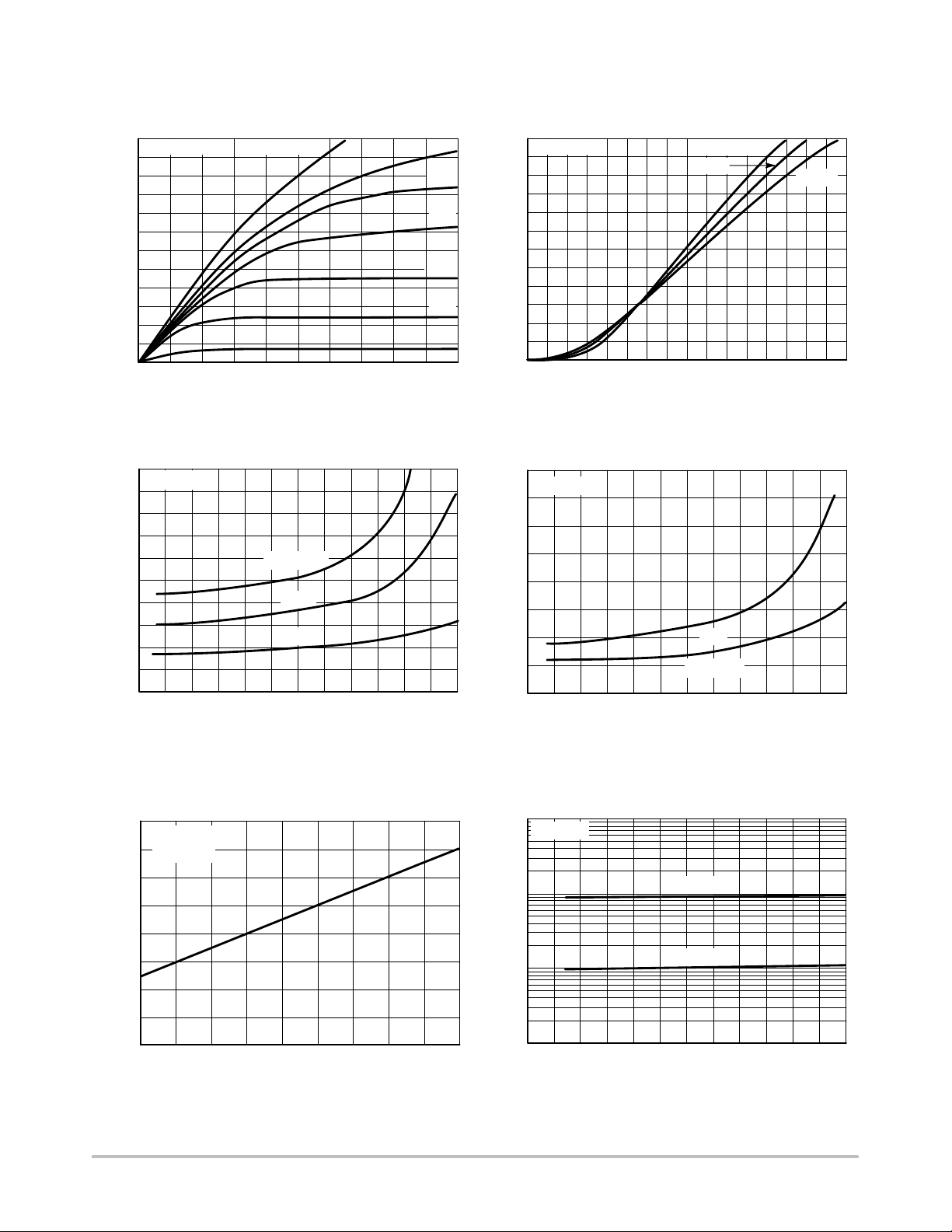
TYPICAL ELECTRICAL CHARACTERISTICS
24
T
= 25°C
J
20
16
12
8
, DRAIN CURRENT (AMPS)
D
I
4
0
01 2 3 5
VDS, DRAIN-TO-SOURCE VOLTAGE (VOLTS)
VGS = 10 V
5 V
4.5 V
3.5 V
2.5 V
4
Figure 1. On–Region Characteristics
0.32
VGS = 5 V
0.26
0.20
0.14
T
= 100°C
J
25°C
4 V
3 V
24
V
≥ 10 V
DS
20
16
12
8
, DRAIN CURRENT (AMPS)
D
I
4
0
2.5 3.5 4.5 5.5
2.0 3.0 4.0 5.0 6.0
VGS, GATE-TO-SOURCE VOLTAGE (VOLTS)
T
= -55°C
J
25°C
Figure 2. Transfer Characteristics
0.27
T
= 25°C
J
0.22
0.17
100°C
0.08
, DRAIN-TO-SOURCE RESISTANCE (OHMS)
DS(on)
0.02
R
0481216 24
ID, DRAIN CURRENT (AMPS)
-55°C
20 8
Figure 3. On–Resistance versus Drain Current
and Temperature
2.0
VGS = 5 V
ID = 6 A
1.5
1.0
(NORMALIZED)
0.5
, DRAIN-TO-SOURCE RESISTANCE
DS(on)
R
0
-50
-25 0 25 50 75 100 125 150
T
, JUNCTION TEMPERATURE (°C)
J
Figure 5. On–Resistance Variation with
Temperature
175
0.12
, DRAIN-TO-SOURCE RESISTANCE (OHMS)
DS(on)
0.07
R
0 4 12 16 20 24
ID, DRAIN CURRENT (AMPS)
5 V
VGS = 10 V
Figure 4. On–Resistance versus Drain Current
and Gate Voltage
100
VGS = 0 V
T
10
, LEAKAGE (nA)
1.0
DSS
I
0.1
01020 405060
VDS, DRAIN-TO-SOURCE VOLTAGE (VOLTS)
= 125°C
J
100°C
30
Figure 6. Drain–To–Source Leakage
Current versus Voltage
http://onsemi.com
3
MTD3055VL
POWER MOSFET SWITCHING
Switching behavior is most easily modeled and predicted
by recognizing that the power MOSFET is charge
controlled. The lengths of various switching intervals (∆t)
are determined by how fast the FET input capacitance can
be charged by current from the generator.
The published capacitance data is difficult to use for
calculating rise and fall because drain–gate capacitance
varies greatly with applied voltage. Accordingly, gate
charge data is used. In most cases, a satisfactory estimate of
average input current (I
) can be made from a
G(AV)
rudimentary analysis of the drive circuit so that
t = Q/I
G(AV)
During the rise and fall time interval when switching a
resistive load, VGS remains virtually constant at a level
known as the plateau voltage, V
. Therefore, rise and fall
SGP
times may be approximated by the following:
tr = Q2 x RG/(VGG – V
tf = Q2 x RG/V
GSP
GSP
)
where
VGG = the gate drive voltage, which varies from zero to V
GG
RG = the gate drive resistance
and Q2 and V
are read from the gate charge curve.
GSP
During the turn–on and turn–off delay times, gate current is
not constant. The simplest calculation uses appropriate
values from the capacitance curves in a standard equation for
voltage change in an RC network. The equations are:
t
d(on)
t
d(off)
= RG C
= RG C
In [VGG/(VGG – V
iss
In (VGG/V
iss
GSP
)]
GSP
)
The capacitance (C
) is read from the capacitance curve at
iss
a voltage corresponding to the off–state condition when
calculating t
on–state when calculating t
and is read at a voltage corresponding to the
d(on)
d(off)
.
At high switching speeds, parasitic circuit elements
complicate the analysis. The inductance of the MOSFET
source lead, inside the package and in the circuit wiring
which is common to both the drain and gate current paths,
produces a voltage at the source which reduces the gate drive
current. The voltage is determined by Ldi/dt, but since di/dt
is a function of drain current, the mathematical solution is
complex. The MOSFET output capacitance also
complicates the mathematics. And finally, MOSFETs have
finite internal gate resistance which effectively adds to the
resistance of the driving source, but the internal resistance
is difficult to measure and, consequently, is not specified.
The resistive switching time variation versus gate
resistance (Figure 9) shows how typical switching
performance is affected by the parasitic circuit elements. If
the parasitics were not present, the slope of the curves would
maintain a value of unity regardless of the switching speed.
The circuit used to obtain the data is constructed to minimize
common inductance in the drain and gate circuit loops and
is believed readily achievable with board mounted
components. Most power electronic loads are inductive; the
data in the figure is taken with a resistive load, which
approximates an optimally snubbed inductive load. Power
MOSFETs may be safely operated into an inductive load;
however, snubbing reduces switching losses.
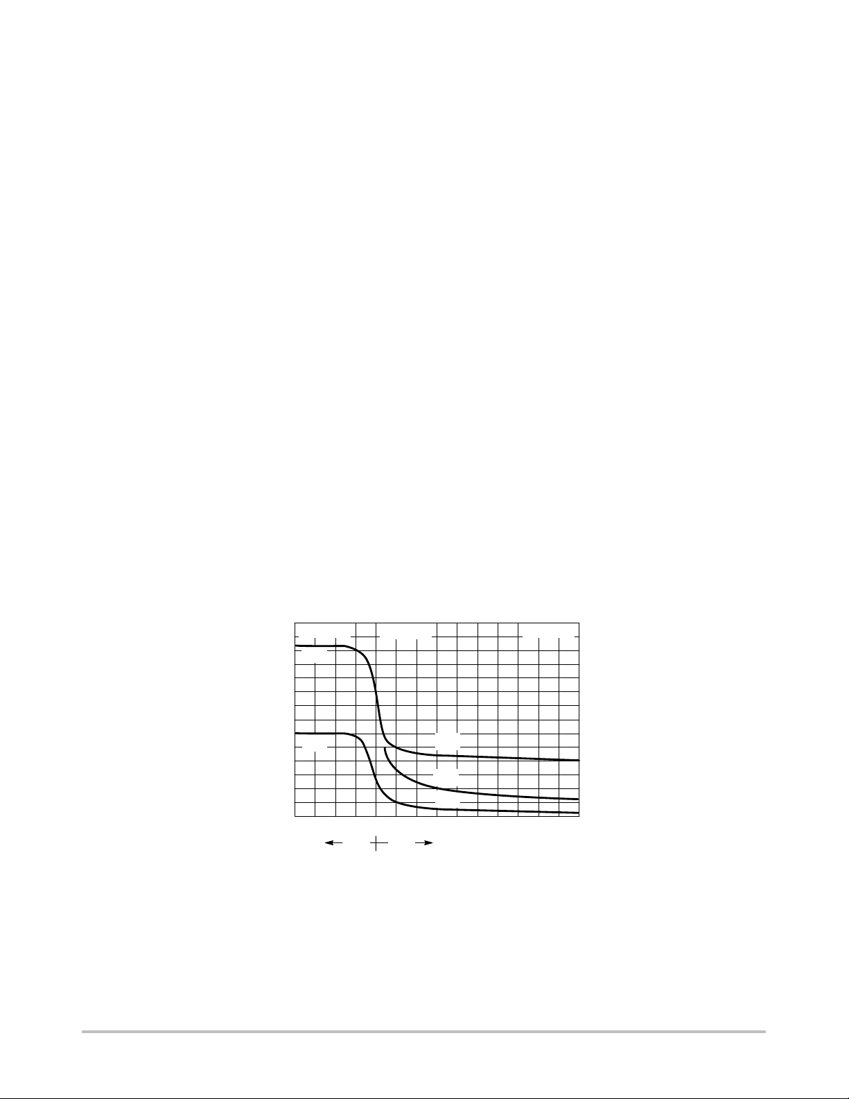
1400
VDS = 0 V
1200
C
iss
1000
800
600
C
rss
400
C, CAPACITANCE (pF)
200
0
10 5 0 10 20 25
GATE-TO-SOURCE OR DRAIN-TO-SOURCE VOLTAGE (VOLTS)
Figure 7. Capacitance Variation
VGS = 0 V
C
iss
C
oss
C
rss
515
V
GS
V
DS
T
= 25°C
J
http://onsemi.com
4
 Loading...