

Motorola MTB10N40E Datasheet
1
Motorola TMOS Power MOSFET Transistor Device Data
$ #
" "!
N–Channel Enhancement–Mode Silicon Gate
The D2PAK package has the capability of housing a larger die
than any existing surface mount package which allows it to be used
in applications that require the use of surface mount components
with higher power and lower R
DS(on)
capabilities. This high voltage
MOSFET uses a n advanced t ermination scheme to p rovide
enhanced voltage–blocking capability without degrading performance over time. In addition, this advanced TMOS E–FET is
designed to withstand high energy in the avalanche and commutation m odes. T he n ew energy efficient design also o ffers a
drain–to–source diode with a fast recovery time. Designed for high
voltage, high speed switching applications in power supplies,
converters and PWM motor controls, these devices are particularly
well suited for bridge circuits where diode speed and commutating
safe operating areas are critical and offer additional safety margin
against unexpected voltage transients.
• Robust High Voltage Termination
• Avalanche Energy Specified
• Source–to–Drain Diode Recovery Time Comparable to a Discrete
Fast Recovery Diode
• Diode is Characterized for Use in Bridge Circuits
• I
DSS
and V
DS(on)
Specified at Elevated Temperature
• Short Heatsink Tab Manufactured — Not Sheared
• Specially Designed Leadframe for Maximum Power Dissipation
• Available in 24 mm 13–inch/800 Unit Tape & Reel, Add T4
Suffix to Part Number
MAXIMUM RATINGS
(TC = 25°C unless otherwise noted)
Rating
Symbol Value Unit
Drain–to–Source Voltage V
DSS
400 Vdc
Drain–to–Gate Voltage (RGS = 1.0 MΩ) V
DGR
400 Vdc
Gate–to–Source Voltage — Continuous V
GS
±20 Vdc
Drain Current — Continuous
Drain Current — Continuous @ 100°C
Drain Current — Single Pulse (tp ≤ 10 µs)
I
D
I
D
I
DM
10
6.0
40
Amps
Apk
Total Power Dissipation
Derate above 25°C
Total Power Dissipation @ TA = 25°C, when mounted with the minimum recommended pad size
P
D
125
1.00
2.5
Watts
W/°C
Watts
Operating and Storage Temperature Range TJ, T
stg
– 55 to 150 °C
Single Pulse Drain–to–Source Avalanche Energy — Starting TJ = 25°C
(VDD = 25 Vdc, VGS = 10 Vpk, IL = 10 Apk, L = 10 mH, RG = 25 Ω)
E
AS
520 mJ
Thermal Resistance — Junction to Case
Thermal Resistance — Junction to Ambient
Thermal Resistance — Junction to Ambient, when mounted with the minimum recommended pad size
R
θJC
R
θJA
R
θJA
1.00
62.5
50
°C/W
Maximum Lead Temperature for Soldering Purposes, 1/8″ from case for 10 seconds T
L
260 °C
Designer’s Data for “Worst Case” Conditions — The Designer’s Data Sheet permits the design of most circuits entirely from the information presented. SOA Limit
curves — representing boundaries on device characteristics — are given to facilitate “worst case” design.
E–FET and Designer’s are trademarks of Motorola, Inc. TMOS is a registered trademark of Motorola, Inc.
Thermal Clad is a trademark of the Bergquist Company
Preferred devices are Motorola recommended choices for future use and best overall value.
Order this document
by MTB10N40E/D
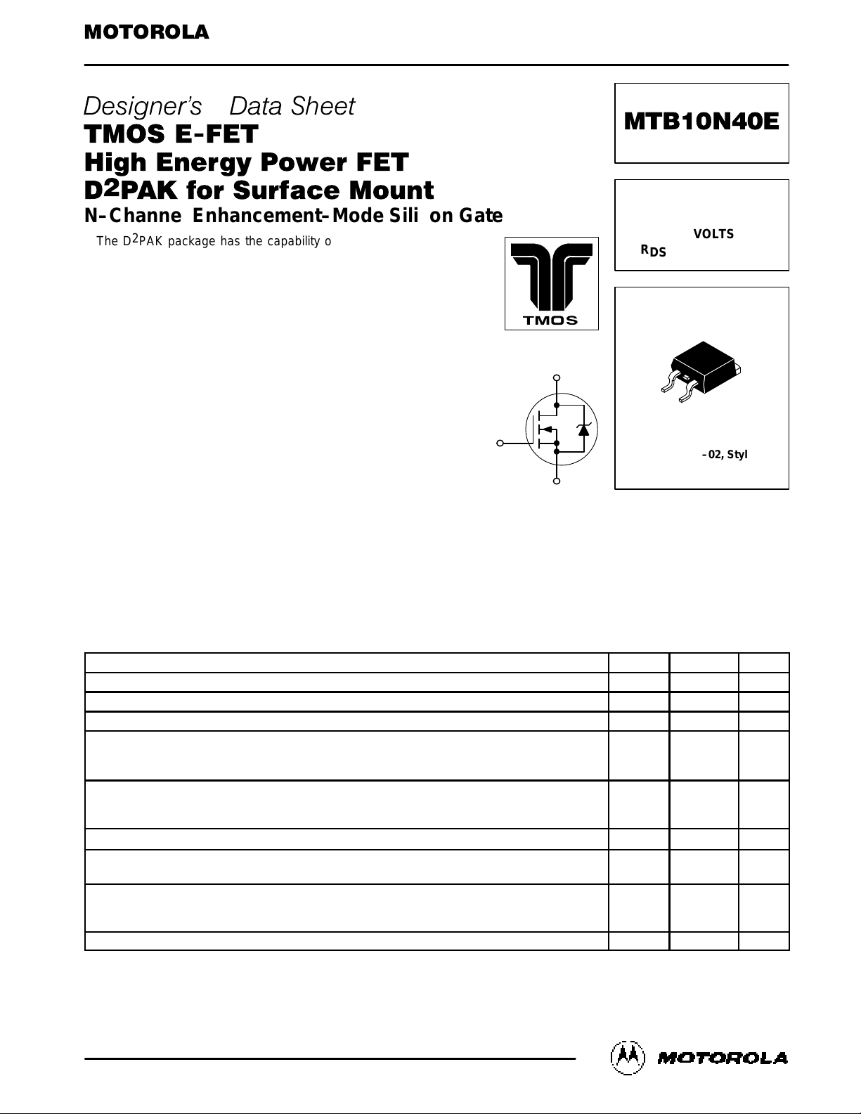
SEMICONDUCTOR TECHNICAL DATA
Motorola, Inc. 1994
TMOS POWER FET
10 AMPERES
400 VOLTS
R
DS(on)
= 0.55 OHM
Motorola Preferred Device
CASE 418B–02, Style 2
D2PAK
D
S
G
MTB10N40E
2
Motorola TMOS Power MOSFET Transistor Device Data
ELECTRICAL CHARACTERISTICS
(T
J
= 25°C unless otherwise noted)
Characteristic
Symbol Min Typ Max Unit
OFF CHARACTERISTICS
Drain–Source Breakdown Voltage
(VGS = 0 Vdc, ID = 250 µAdc)
Temperature Coefficient (Positive)
V
(BR)DSS
400
—
—
398
—
—
Vdc
mV/°C
Zero Gate Voltage Drain Current
(VDS = 400 Vdc, VGS = 0 Vdc)
(VDS = 400 Vdc, VGS = 0 Vdc, TJ = 125°C)
I
DSS
—
—
—
—
0.1
1.0
µAdc
Gate–Body Leakage Current–Forward
(V
gsf
= 20 Vdc, VDS = 0)
I
GSSF
— — 100 nAdc
Gate–Body Leakage Current–Reverse
(V
gsr
= 20 Vdc, VDS = 0)
I
GSSR
— — 100 nAdc
ON CHARACTERISTICS (1)
Gate Threshold Voltage
(VDS = VGS, ID = 250 µAdc)
Temperature Coefficient (Negative)
V
GS(th)
2.0
—
2.8
6.3
4.0
—
Vdc
mV/°C
Static Drain–Source On–Resistance (VGS = 10 Vdc, ID = 5.0 Adc) R
DS(on)
— 0.4 0.55 Ohm
Drain–Source On–Voltage (VGS = 10 Vdc)
(ID = 10 Adc)
(ID = 5.0 Adc, TJ = 125°C)
V
DS(on)
—
—
5.61
—
6.6
5.5
Vdc
Forward Transconductance (VDS = 15 Vdc, ID = 5.0 Adc) g
FS
4.0 — — mhos
DYNAMIC CHARACTERISTICS
Input Capacitance
C
iss
— 1570 2200 pF
Output Capacitance
(VDS = 25 Vdc, VGS = 0 Vdc,
f = 1.0 MHz)
C
oss
— 230 325
Reverse Transfer Capacitance
f = 1.0 MHz)
C
rss
— 55 110
SWITCHING CHARACTERISTICS (2)
Turn–On Delay Time
t
d(on)
— 25 50 ns
Rise Time
t
r
— 37 75
Turn–Off Delay Time
VGS = 10 Vdc,
RG = 10 Ω)
t
d(off)
— 75 150
Fall Time
G
= 10 Ω)
t
f
— 31 65
Q
T
— 46 63 nC
(See Figure 8)
DS
= 320 Vdc, ID = 10 Adc,
Q
1
— 10 —
(VDS = 320 Vdc, ID = 10 Adc,
VGS = 10 Vdc)
Q
2
— 23 —
Q
3
— — —
SOURCE–DRAIN DIODE CHARACTERISTICS
Forward On–Voltage (1)
(IS = 10 Adc, VGS = 0 Vdc)
(IS = 10 Adc, VGS = 0 Vdc, TJ = 125°C)
V
SD
—
—
0.9
—
2.0
—
Vdc
Reverse Recovery Time
(See Figure 14)
t
rr
— 250 — ns
Reverse Recovery Stored Charge
dIS/dt = 100 A/µs)
Q
RR
— 3000 — nC
INTERNAL PACKAGE INDUCTANCE
Internal Drain Inductance
(Measured from the tab to center of die)
(Measured from the drain lead 0.25″ from package to center of die)
L
D
—
—
3.5
4.5
—
—
nH
Internal Source Inductance
(Measured from the source lead 0.25″ from package to source bond pad)
L
S
— 7.5 — nH
(1) Pulse Test: Pulse Width ≤ 300 µs, Duty Cycle ≤ 2%.
(2) Switching characteristics are independent of operating junction temperature.
Gate Charge
(VDD = 200 Vdc, ID = 10 Adc,
(V
(IS = 10 Adc, VGS = 0 Vdc,
MTB10N40E
3
Motorola TMOS Power MOSFET Transistor Device Data
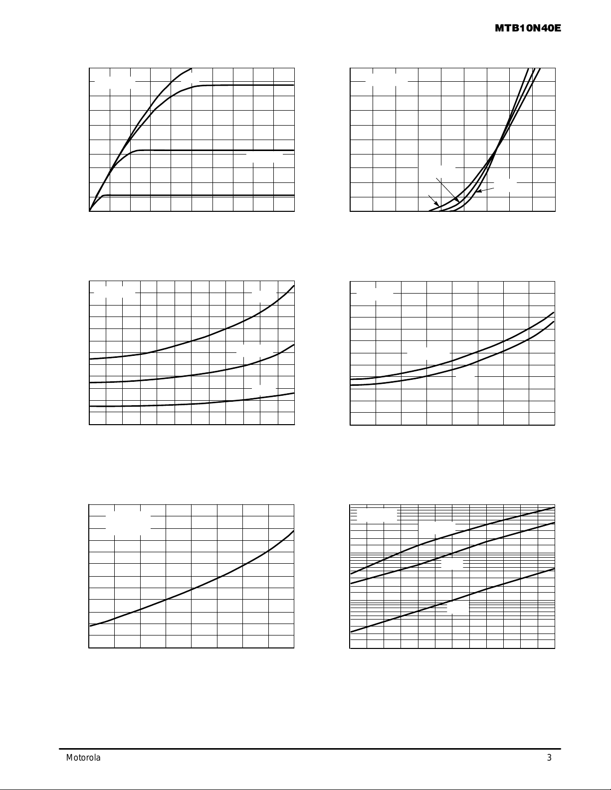
TYPICAL ELECTRICAL CHARACTERISTICS
1
3
2
0
–50 –25 0 25 50 75 100 125 150
VGS = 10 V
TJ = 25°C
100°C
–55°C
0
0.5
1
1.5
0 5 10 15 20 25 30
0
10
15
20
25
5
0 1 4 6 7 92 3 5 8
VDS ≥
10 V
TJ = 25°C
100°C
–55°C
10 V
7 V
5 V
VGS = 6 V
0
8
12
16
20
4
0 4 8 12 16 20
TJ = 25°C
VDS, DRAIN–TO–SOURCE VOLTAGE (VOLTS)
Figure 1. On–Region Characteristics
I
D
, DRAIN CURRENT (AMPS)
I
D
, DRAIN CURRENT (AMPS)
VGS, GATE–TO–SOURCE VOLTAGE (VOLTS)
Figure 2. Transfer Characteristics
ID, DRAIN CURRENT (AMPS)
Figure 3. On–Resistance versus Drain Current
and Temperature
Figure 4. On–Resistance versus Drain Current
and Gate Voltage
TJ, JUNCTION TEMPERATURE (°C)
Figure 5. On–Resistance Variation with
Temperature
0.55
0.5
0.45
0.4
0.35
0.3
0.25
0
ID, DRAIN CURRENT (AMPS)
5 10 15 20
VGS = 10 V
15 V
TJ = 25°C
VDS, DRAIN–TO–SOURCE VOLTAGE (VOLTS)
Figure 6. Drain–To–Source Leakage
Current versus Voltage
I
DSS
, LEAKAGE (nA)
100
100
10
1
0.1
150 200 250 300 350 400
100°C
25°C
TJ = 125°C
VGS = 0 V
VGS = 10 V
ID = 5 A
0.2
0.4
2
4
20
40
, DRAIN–TO–SOURCE RESISTANCE (OHMS)
DS(on)
R
, DRAIN–TO–SOURCE RESISTANCE (OHMS)
DS(on)
R
(NORMALIZED)
, DRAIN–TO–SOURCE RESISTANCE
DS(on)
R
 Loading...