Motorola MRFIC1803 Datasheet

SEMICONDUCTOR TECHNICAL DATA
The MRFIC Line
Designed primarily for use in DECT , Japan’ s Personal Handy System (PHS),
and other wireless Personal Communication Systems (PCS) applications at 1.8
GHz, but also applicable to Industrial, Scientific and Medical (ISM) applications
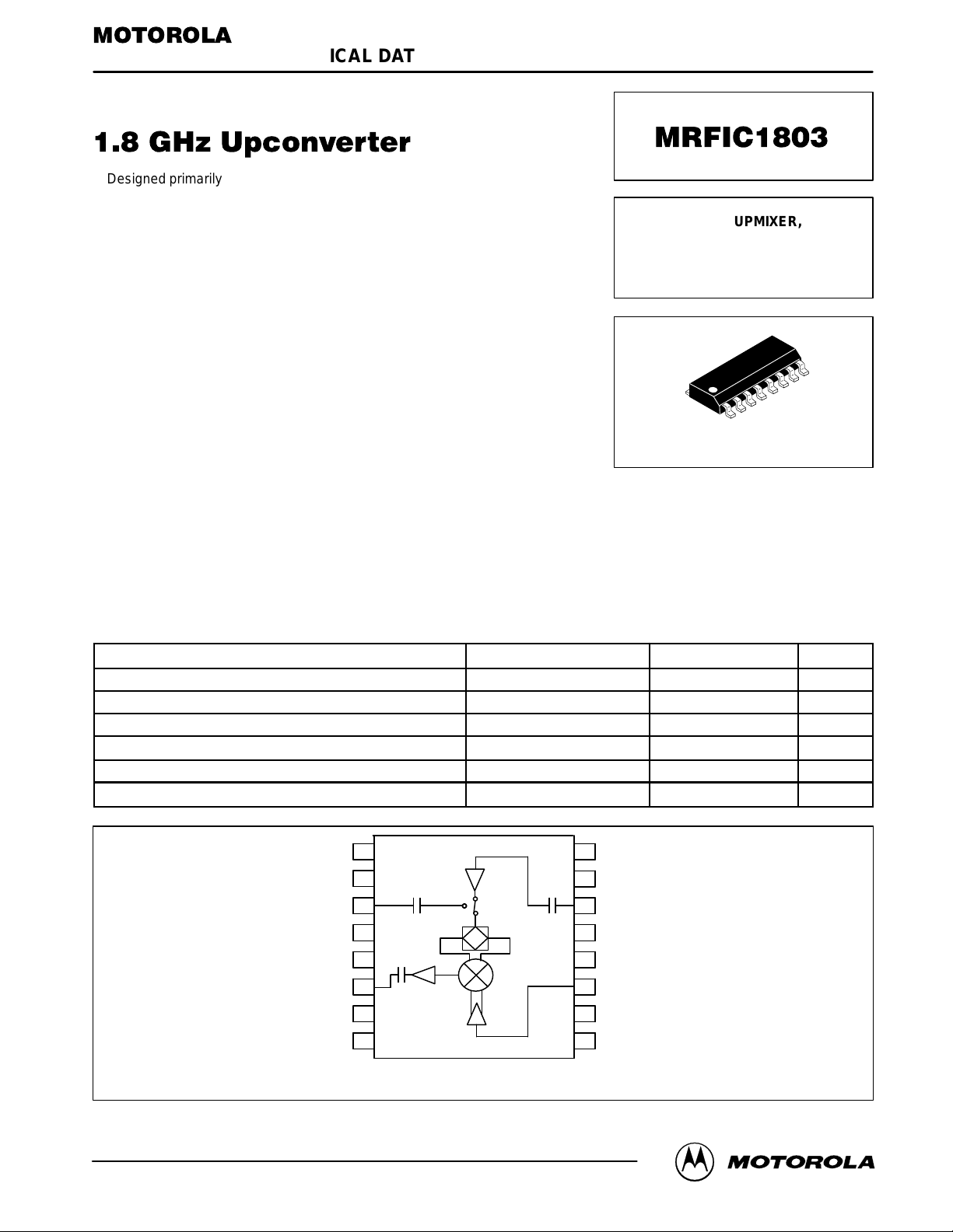
at 2.5 GHz. The MRFIC1803 is a complete active upmixer, exciter amplifier , and
LO buffer amplifier in a low-cost SOIC-16 package. The low power consumption
design includes a single balanced active mixer, CMOS compatible receive and
transmit enable inputs, a buffer/exciter amplifier, and a buffered LO output
capable of driving the MRFIC1804 downconverter. IF, LO and RF ports are
matched to 50 Ω and no off-chip baluns are required. With both TX and RX
enable pins low, the device is in standby mode and draws less than 0.3 mA.
Together with the rest of the MRFIC180X series, this GaAs IC family offers
the complete transmit and receive functions, less LO and filters, needed for a
typical 1.8 GHz cordless telephone.
• 10 dB IF to RF Conversion Gain
• Usable Frequency Range = 1.7 to 2.5 GHz
• Low Power Consumption = 80 mW (Typ)
• Single Bias Supply = 2.7 to 3.3 V
• No External Baluns Required
• IF, LO and RF Ports Matched to 50 Ω
• Low LO Power Requirement = –10 dBm (Typ)
• Low Cost Surface Mount Plastic Package
• Order MRFIC1803R2 for Tape and Reel.
R2 Suffix = 2,500 Units per 16 mm, 13 inch Reel.
• Device Marking = M1803
Order this document
by MRFIC1803/D
1.8 GHz UPMIXER,
EXCITER AND LO AMP
GaAs MONOLITHIC
INTEGRATED CIRCUIT
CASE 751B-05
(SO–16)
MAXIMUM RATINGS
(TA = 25°C unless otherwise noted)
Ratings Symbol Value Unit
Supply Voltage V
IF Input Power P
LO Input Power P
Transmit and Receive Enable V oltage
Storage Temperature Range T
Operating Ambient Temperature T
1GND
GND
LO OUT
GND
GND
RF OUT
GND
V
DD
LO BUFFER
2
AND SWITCH
3
4
EXCITER
5
6
ACTIVE
7
BALANCED
MIXER
8
TX EN, RX EN 5.5
DD
IF
LO
stg
A
16
15
14
13
12
11
10
9
5.5 Vdc
3 dBm
3 dBm
Vdc
– 65 to +150 °C
– 30 to + 85 °C
RX EN
GND
LO IN
GND
GND
IF IN
GND
TX EN
REV 3
Motorola, Inc. 1997
Pin Connections and Functional Block Diagram
MRFIC1803MOTOROLA RF DEVICE DATA
1

RECOMMENDED OPERATING RANGES
Parameter
LO Input Frequency f
LO Input Power P
IF Input Frequency f
RF Output Frequency f
Transmit and Receive Enable V oltage TX EN, RX EN 2.7 to V
Supply Voltage V
Symbol Value Unit
LO
LO
IF
RF
DD
1.5 to 2.4 GHz
70 to 350 MHz
1.7 to 2.5 GHz
2.7 to 5 Vdc
–10 dBm
DD
Vdc
ELECTRICAL CHARACTERISTICS (V
TX EN = 3.0 V, RX EN = 0 V, unless otherwise noted)
Characteristic
IF to RF Conversion Gain 8 10 — dB
RF Output 1 dB Compression — –2 — dBm
RF Output 3rd Order Intercept — 9 — dBm
LO Feed Through to RF Port — –19 — dBm
Auxiliary LO Output Power (TX EN = 0 V, RX EN = 3 Vdc) — –4 — dBm
Supply Current, TX Mode — 28 50 mA
Supply Current, RX Mode (TX EN = 0 V, RX EN = 3 Vdc) — 3 — mA
Standby Mode Current (TX EN = 0 V, RX EN = 0 Vdc) — 0.1 0.3 mA
= 3 V, TA = 25°C, LO = 1790 MHz @ –10 dBm, IF = 110 MHz @ –15 dBm,
DD
Min Typ Max Unit
RX EN LO IN IF IN TX EN
C1
15
1416
10 9111213
MRFIC1803
2
1
2
345678
LO OUT RF OUT V
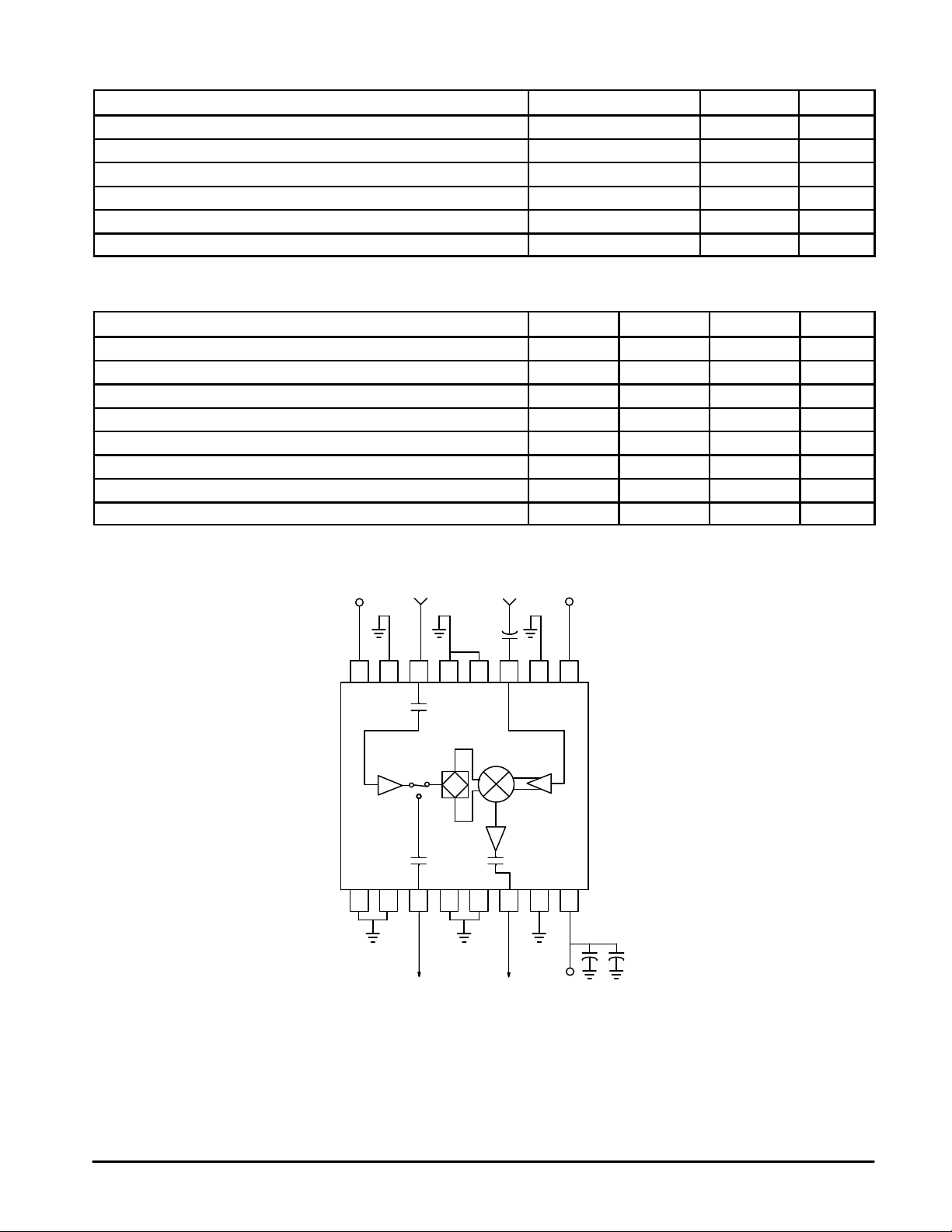
C1 470 pF
C2 100 pF
C3 0.1 µF (optional)
DD
Figure 1. Applications Circuit Configuration
C2
C3
MOTOROLA RF DEVICE DATA
 Loading...