Motorola MRFIC1502 Datasheet

SEMICONDUCTOR TECHNICAL DATA
The MRFIC Line
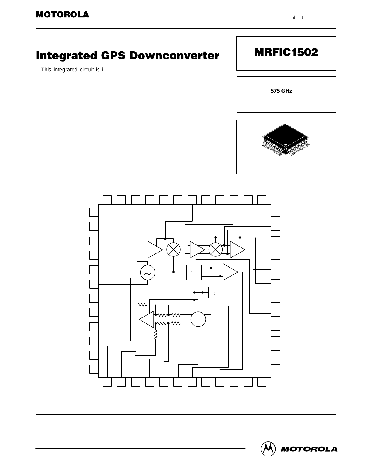
This integrated circuit is intended for GPS receiver applications. The dual
conversion design is implemented in Motorola’s low–cost high performance
MOSAIC 3 silicon bipolar process and is packaged in a low–cost surface mount
TQFP–48 package. In addition to the mixers, a VCO, a PLL and a loop filter are
integrated on–chip. Output IF is nominally 9.5 MHz.
• 65 dB Minimum Conversion Gain
• 5 Volts Operation
• 50 mA Typical Current Consumption
• Low–Cost, Low Profile Plastic TQFP Package
• Device Marking = M1502
GND GND GND GND RF IN GND V
48 47 46 45 44 43 42 41 40 39 38 37
CC1
GND
BPF
TO
FROM
BPF
Order this document
by MRFIC1502/D
1.575 GHz GPS
DOWNCONVERTER
CASE 932–02
(TQFP–48)
GND GND
GND
VCO VT
GND
V
CC5
GND
VCO CE
GND
SF CAP1
GND
SF CAP2
GND
GND
TQFP–48
1
2
3
4
5
6
7
8
9
10
11
12
ACTIVE
FILTER
LOOP
FILTER
13 14 15 16 17 18 19
C2A C2B C1 CA CB DCX0 V
VCO
40
PHASE
DETECTOR
20 21 22 23
GND CLK
CC4
2
OUT
GND GND
24
GND
GND
36
35
38 MHz TRAP
38 MHz TRAP
34
33
BYPASS CAP
32
IF OUT
31
V
CC2
GND
30
GAIN CONTROL
29
V
28
CC3
GND
27
GND
26
GND
25
Motorola, Inc. 1997
MOTOROLA RF DEVICE DATA
Pin Connections and Functional Block Diagram
MRFIC1502
1

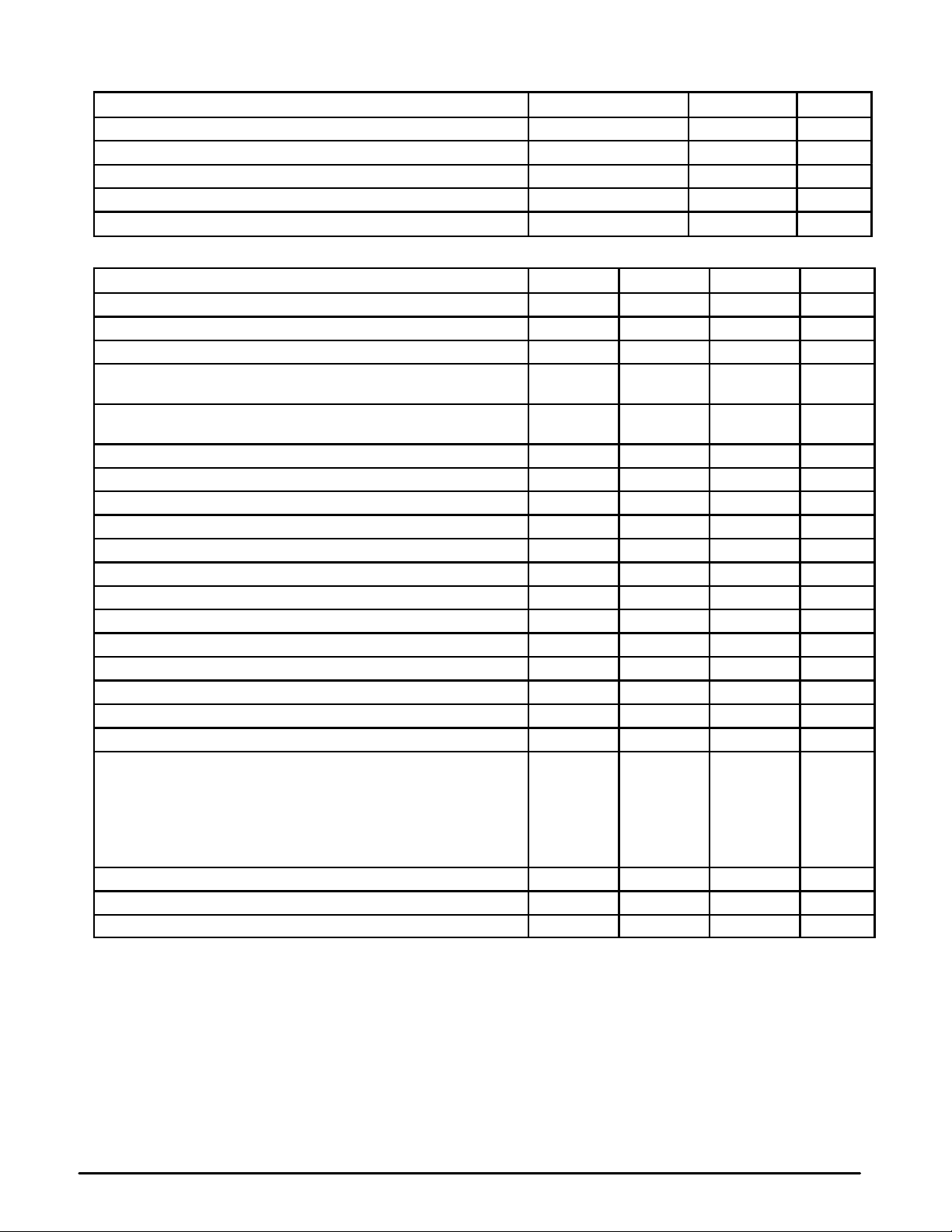
MAXIMUM RATINGS
Rating Symbol Limit Unit
DC Supply Voltage V
DC Supply Current I
Operating Ambient Temperature T
Storage Temperature Range T
Lead Soldering Temperature Range (10 seconds) — +260 °C
DD
DD
A
stg
+6.0 Vdc
60 mA
– 40 to +100 °C
– 65 to +150 °C
ELECTRICAL CHARACTERISTICS (T
Characteristic
Supply Voltage 4.75 — 5.25 Vdc
Supply Current — — 60 mA
L–Band Gain (Measured from L–Band Input to 47 MHz Output) — 20 — dB
IF Gain (Measured from 47 MHz Input to 9.5 MHz Output with Gain
Control at Maximum)
Conversion Gain (Measured from L–Band Input to 9.5 MHz Output with
Gain Control at Maximum)
Gain Control (Externally Adjustable 0 to 5.0 V , Maximum at 0 V) — 40 — dB
Noise Figure (Double Sideband) — 9.5 — dB
L–Band Input VSWR (Measured into 50 Ω; 1575.42 ± 5.0 MHz) — 2:1 — —
First IF Output VSWR (Measured into 50 Ω; 47.74 ± 5.0 MHz) — 2:1 — —
Second IF Output VSWR (Measured into 50 Ω; 9.5 ± 5.0 MHz) — 2:1 — —
Input Impedance @ 1st IF 47.7 ± 5 MHz (For Reference Only) — 2000 — Ω
Output 1.0 dB Compression Point — –7 — dBm
First LO (Measured at the First IF Output) — –20 — dBm
All Other Harmonics (Measured at the First IF Output) — –45 — dBm
38.1915 MHz Leakage at First IF Output — –50 — dBm
Second LO (Measured at the Second IF Output) — –25 — dBm
All Other Harmonics (Measured at Second IF Output) — –45 — dBm
Reference Oscillator Input 400 — 4500 mVpp
Clock Output
Frequency
Amplitude
Low
HIgh
(Clock Amplitude Measured with the Output Loaded in 15 pF and 40 kΩ)
Duty Cycle
VCO Lock Voltage 1.2 — 3.0 V
Phase Detector Gain — 0.16 — V/Radian
VCO Modulation Sensitivity — 15 — MHz/V
= 25°C, and VCC = 5 V, Tested in Circuit shown in Figure 1 unless otherwise noted)
A
Min Typ Max Unit
— 45 — dB
65 — — dB
2Xf
ref
—
2.0
45
— 2Xf
ref
0.8
—
55
V
V
%
MRFIC1502
2
MOTOROLA RF DEVICE DATA

L7
C21C22
CR1
C31
C23
V
CC
RF
INPUT
C18
48 47 46 45 44 43 42
TQFP–48
1
C17
L3
R1
V
CC
L1
C15
C35
C16
2
3
4
5
6
7
ACTIVE
FILTER
VCO
L10
C19
40
L8
L9
C24
C34
41 40 39 38
2
L6
C20
R3
37
36
35
34
33
C12
32
IF OUTPUT
31
C10 C1 1
30
C14
C36 C13
V
L5
CC
8
C3
10
C2
11
12
C1, C8, C10, C12, C13, C15,
C19, C20, C37 10,000 pF
C4, C5 5600 pF
C6, C7, C31 1000 pF
C2, C3 1.0 µF
C14 3.9 pF, ATC
C16, C18, C36 27 pF, ATC
C17 15 pF, ATC
C21 5.6 pF, ATC
C9, C11, C34, C36 47 pF, ATC
C22, C23 120 pF, A TC
LOOP
9
FILTER
13 14 15 16 17 18 19
C5 C6 C7 C1
C4
29
PHASE
DETECTOR
20 21 22 23
L1
DXCO
C36 C37
V
CC
C24 68 pF, ATC
C35 0.4 pF, ATC
CR1 2.7 pF , MA45233–123, MACOM
L1, L4, L5, L10 2.2 µH, 1008CS–222XKBC, COILCRAFT
L3 2.2 nH, LL2012–F2N2S, TOKO
L6 2.2 µH
L7 220 nH
L8 0.56 µH
L9 0.27 µH
R1 10 kΩ
R3 220 Ω
CLOCK
OUTPUT
28
27
26
25
24
GAIN CONTROL
C8 C9
L4
V
CC
MOTOROLA RF DEVICE DATA
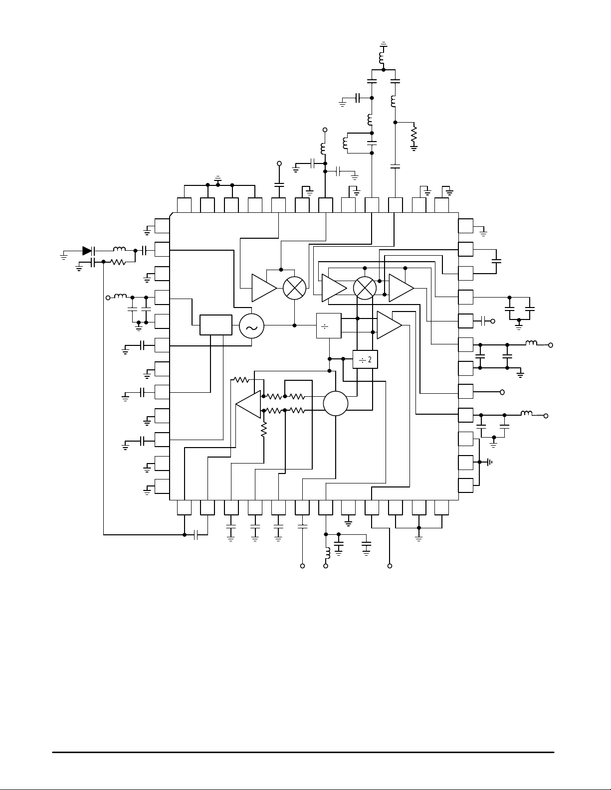
Figure 1. T est Circuit Configuration
MRFIC1502
3
 Loading...