Motorola MRFIC1501 Datasheet

SEMICONDUCTOR TECHNICAL DATA
The MRFIC Line
Order this document
by MRFIC1501/D
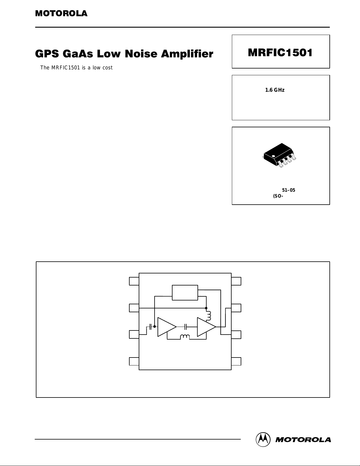
The MRFIC1501 is a low cost yet high performance two–stage, low–noise
amplifier designed primarily for use in Global Positioning Satellite System
(GPS) and other L–band satellite receivers. The broadband nature of the design
makes the device applicable to a variety of L–band applications where high
performance at reasonable current and cost are required. Supply current is
minimized through a current sharing DC cascode circuit configuration. Supply
voltage can be applied to either the VDD pin or the RF output pin for remote
antenna applications. The integrated circuit requires minimal off-chip matching
while allowing for maximum flexibility in optimizing gain and noise figure. An
ENABLE pin is provided to allow for a reduced supply current standby mode.
The design employs Motorola’s low cost planar self–aligned MESFET process
to assure repeatable characteristics at minimal cost.
• Usable Frequency Range = 1 to 2 GHz
• 18 dB Typ Gain at VDD = 5 Volts
• 1.1 dB Typ Noise Figure at VDD = 5 Volts
• Simple Off-chip Matching for Maximum Gain/Noise Figure Flexibility
• Single Bias Supply = 3 to 5 Volts
• Low Power Consumption = 30 mW (Typ) at 5 Volts
• Low Cost Surface Mount Plastic Package
• Order MRFIC1501R2 for T ape and Reel Option.
R2 Suffix = 2,500 Units per 12 mm, 13 inch Reel.
• Device Marking = M1501
1.6 GHz GaAs
LOW NOISE
AMPLIFIER
CASE 751–05
(SO-8)
Motorola, Inc. 1996
MOTOROLA RF DEVICE DATA
1
GND
BIAS
2
DD
3
RF IN
GND
4
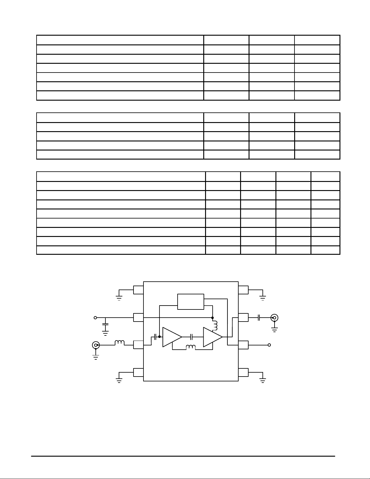
Pin Connections and Functional Block Diagram
8
GND
7
RF OUTV
6
ENABLE
2nd STAGE GND
5
MRFIC1501
1

MAXIMUM RATINGS
(TA = 25°C unless otherwise noted)
Ratings Symbol Limit Unit
Supply Voltage V
RF Input Power P
ENABLE Voltage ENABLE 6 Vdc
VDD Current Sourcing (With Supply Connected to Pin 7) I
Storage Temperature Range T
Operating Ambient Temperature T
DD
RF
PIN2
stg
A
6 Vdc
3 dBm
20 mA
– 65 to +150 °C
– 30 to +100 °C
RECOMMENDED OPERATING RANGES
Parameter
RF Frequency f
ENABLE “ON” (Device Operational) Voltage ENABLE VDD ± 0.5 Vdc
ENABLE “OFF” (Device in Standby Mode) Voltage ENABLE 0 to 0.5 Vdc
Supply Voltage V
Symbol Value Unit
RF
DD
1 to 2 GHz
3 to 5 Vdc
ELECTRICAL CHARACTERISTICS (V
Characteristic
RF Gain 17 18 — dB
SSB Noise Figure — 1.1 — dB
RF Output 3rd Order Intercept Point — 10 — dBm
Output 1 dB Gain Compression — 0 — dBm
Reverse Isolation (s12) — 30 — dB
Input Return Loss — 10 — dB
Output Return Loss — 10 — dB
Supply Current — 5.9 7.5 mA
V
DD
C1
L1
RF IN
= 5 V, TA = 25°C, RF = 1.575 GHz, ENABLE = 5 V, Circuit Configuration Shown in Figure 1)
DD
Min Typ Max Unit
1
BIAS
2
3
8
C2
7
6
RF OUT
ENABLE
MRFIC1501
2
4
C1, C2 – 22 pF
L1 – 11 nH (Implemented in Microstrip)
Figure 1. Applications Circuit Configuration
5
MOTOROLA RF DEVICE DATA

TYPICAL CHARACTERISTICS
24
22
20
–30°C
18
16
SMALL SIGNAL GAIN (dB)
14
12
VDD = 5 V
ENABLE = 5 V
100°C
TA = 25°C
150013001100 1700 1900
f, FREQUENCY (MHz)
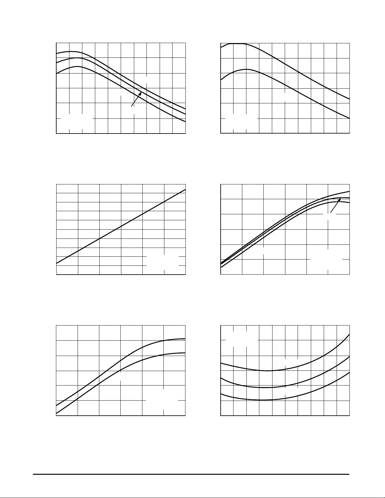
Figure 2. Small Signal Gain versus Frequency
7
6.5
6
5.5
5
4.5
4
, SUPPLY CURRENT (mA)
3.5
DD
3
2.5
2
VDD, DRAIN VOLTAGE (VOLTS)
TA = 25°C
ENABLE = V
DD
54.543.53
22
20
18
16
14
SMALL SIGNAL GAIN (dB)
12
200018001600140012001000
5.52.5 –40
10
5
0
–5
–10
–15
, OUTPUT POWER (dBm)
out
P
–20
–25
5 V
VDD = 3 V
TA = 25°C
ENABLE = V
DD
1800160014001200 150013001100 1700 1900
f, FREQUENCY (MHz)
Figure 3. Small Signal Gain versus Frequency
–30°C
25°C
TA = 100°C
Pin, INPUT POWER (dBm)
VDD = 5 V
ENABLE = 5 V
f = 1575 MHz
– 20 –15
20001000
–10–25–30–35
Figure 4. Drain Current versus Drain Voltage
5
0
–5
–10
–15
, OUTPUT POWER (dBm)
out
P
–20
–25
Pin, INPUT POWER (dBm)
Figure 6. Output Power versus Input Power Figure 7. Noise Figure versus Frequency
MOTOROLA RF DEVICE DATA
5 V
VDD = 3 V
TA = 25°C
ENABLE = V
f = 1575 MHz
– 20 –15–40
DD
Figure 5. Output Power versus Input Power
3
VDD = 5 V
2.5
ENABLE = 5 V
2
100°C
1.5
1
NF, NOISE FIGURE (dB)
0.5
0
–10–25–30–35
1000
f, FREQUENCY (MHz)
25°C
TA = – 30°C
1800160014001200 150013001100 1700 1900
2000
MRFIC1501
3
 Loading...