Motorola MRFIC0916 Datasheet

SEMICONDUCTOR TECHNICAL DATA
The MRFIC Line
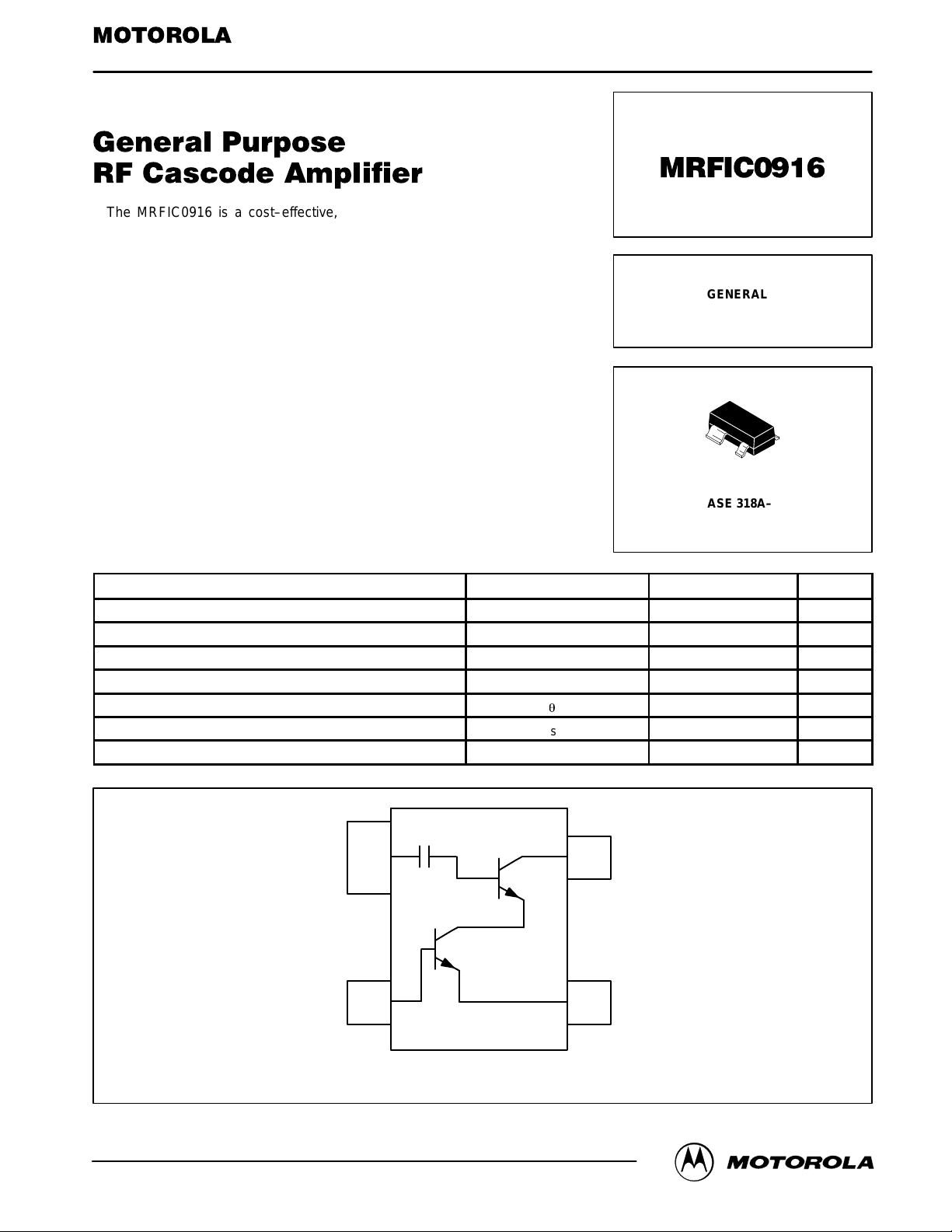
The MRFIC0916 is a cost–effective, high isolation cascode silicon monolithic amplifier in the industry standard SOT–143 surface mount package designed for general purpose RF applications. On chip bias circuitry sets the
bias point while matching is accomplished off chip affording the maximum in
application flexibility.
• Usable Frequency Range = 100 to 2500 MHz
• 18.5 dB typical gain at 850 MHz, VCC = 2.7 Volts
• 2.3 dBm typical Output Power at 1 dB Gain Compression at
850 MHz, VCC = 2.7 Volts
• 44 dB Typical Reverse Isolation at 850 MHz
• 5.6 mA Max Bias Current at VCC = 2.7 Volts
• 2.7 to 5 Volt Supply
• Available in Tape and Reel by Adding T1 Suffix to Part Number.
T1 Suffix = 3,000 Units per 8 mm, 7 inch Reel.
• Device Marking = 16
Order this document
by MRFIC0916/D
SILICON GENERAL PURPOSE
RF CASCODE AMPLIFIER
MAXIMUM RATINGS
Supply Voltage V
RF Input Power P
Power Dissipation P
Supply Current I
Thermal Resistance, Junction to Case
Storage Temperature Range T
Operating Case Temperature T
(TA = 25°C unless otherwise noted)
Rating Symbol Limit Unit
GND
1
CASE 318A–05
(SOT–143)
CC
RF
DIS
CC
R
q
JC
stg
C
3
RF OUT
6 Vdc
10 dBm
100 mW
20 mA
250 °C/W
– 65 to +150 °C
– 35 to +100 °C
REV 1
Motorola, Inc. 1997
RF IN
2
Pin Connections and Functional Block Diagram
4
GND
MRFIC0916MOTOROLA RF DEVICE DATA
1

RECOMMENDED OPERATING RANGES
Parameter
RF Frequency f
Supply Voltage V
Symbol Value Unit
RF
CC
100 to 2500 MHz
2.7 to 5 Vdc
ELECTRICAL CHARACTERISTICS (V
Characteristic
Small Signal Gain 16.5 18.5 20.5 dB
Noise Figure — 1.9 — dB
Power Output at 1dB Gain Compression 0 2.3 — dBm
Output 3rd Order Intercept Point — 11 — dBm
Reverse Isolation — 44 — dB
Supply Current 3.8 4.7 5.6 mA
= 2.7 V, TA = 25°C, fRF = 850 MHz, Tested in Circuit Shown in Figure 1)
CC
Min Typ Max Unit
V
CC
C2
1
C1
L1
C3
3
RF OUT
RF IN
C4
L2
2
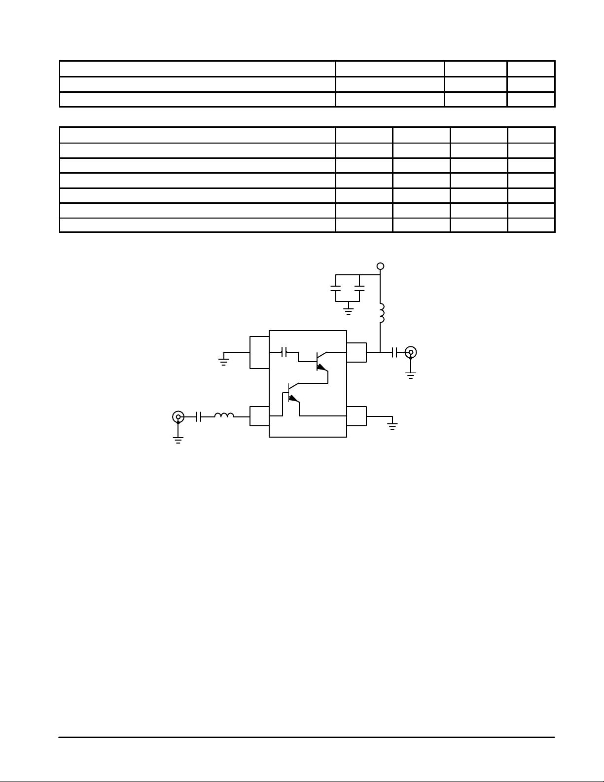
C1 – 100 pF
C2 – 0.01
C3 – 1.4 pF
C4 – 100 pF
L1 – 8.2 nH
L2 – 6.8 nH
µ
4
F
Figure 1. 850 MHz Applications Circuit Configuration
MRFIC0916
2
MOTOROLA RF DEVICE DATA

max
GU , MAXIMUM UNILATERAL GAIN (dB)
40
35
30
25
20
15
10
15
50 W SYSTEM
TA = 25
_
5 V
4 V
VCC = 2.7 V
5
0
0.5 1.0 1.5 2.0 2.5
f, FREQUENCY (GHz)
C
10
5
0
–5
, OUTPUT POWER (dBm)
out
P
–10
–15
–30
–25
5 V
VCC = 2.7 V
–20 –15 –10 –5 0
Pin, INPUT POWER (dBm)
4 V
f = 850 MHz
TA = 25
_
C
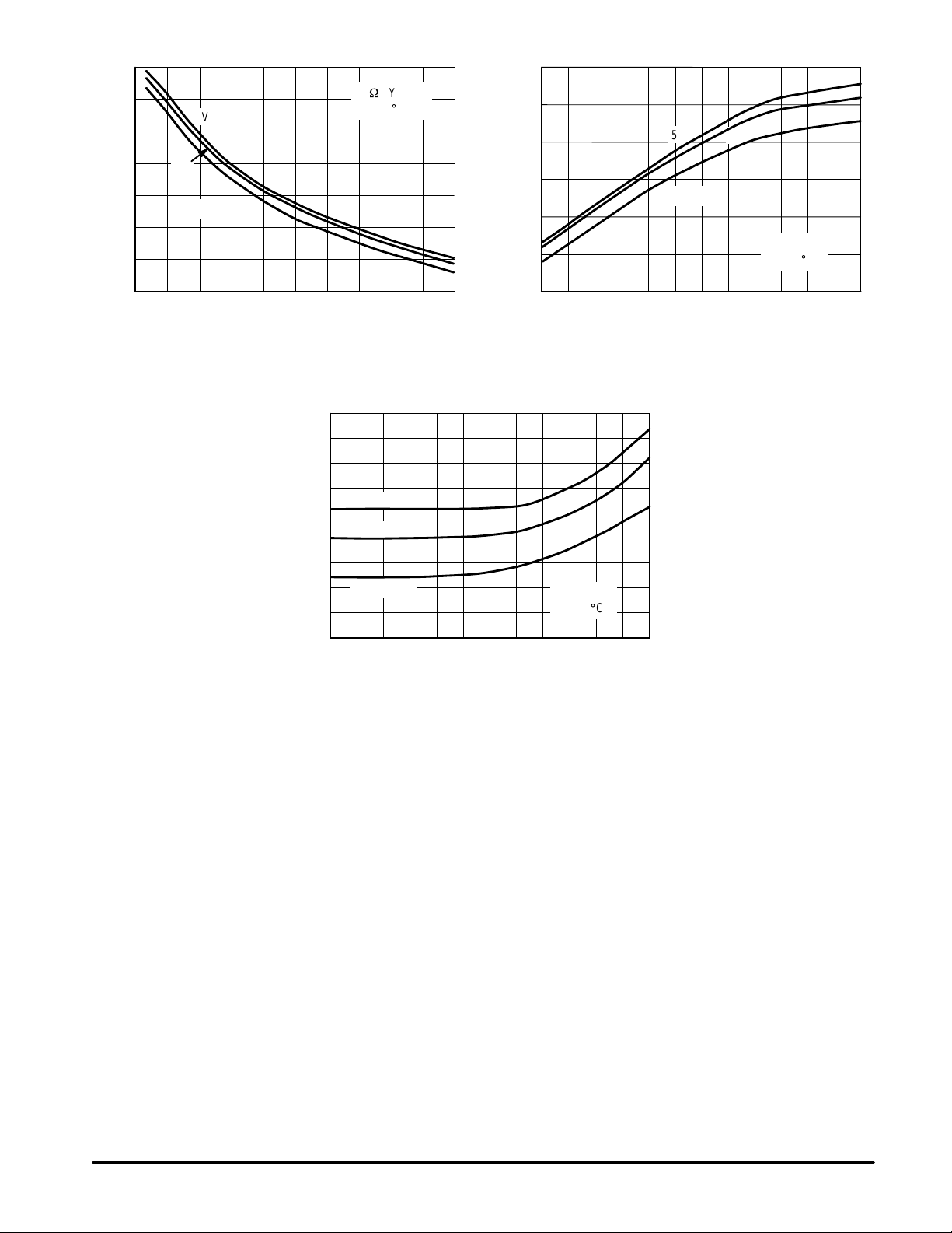
Figure 2. GU
versus Frequency
max
18
16
14
12
10
8
6
CC
4
I , SUPPLY CURRENT (mA)
2
0
–30 0–25 –20 –15 –10 –5
Figure 4. Supply Current versus Input Power
5 V
4 V
VCC = 2.7 V
f = 850 MHz
TA = 25
Pin, INPUT POWER (dBm)
Figure 3. Output Power versus Input Power
_
C
MRFIC0916MOTOROLA RF DEVICE DATA
3
 Loading...