Motorola MRFIC0914 Datasheet

SEMICONDUCTOR TECHNICAL DATA
The MRFIC Line
Order this document
by MRFIC0914/D
!
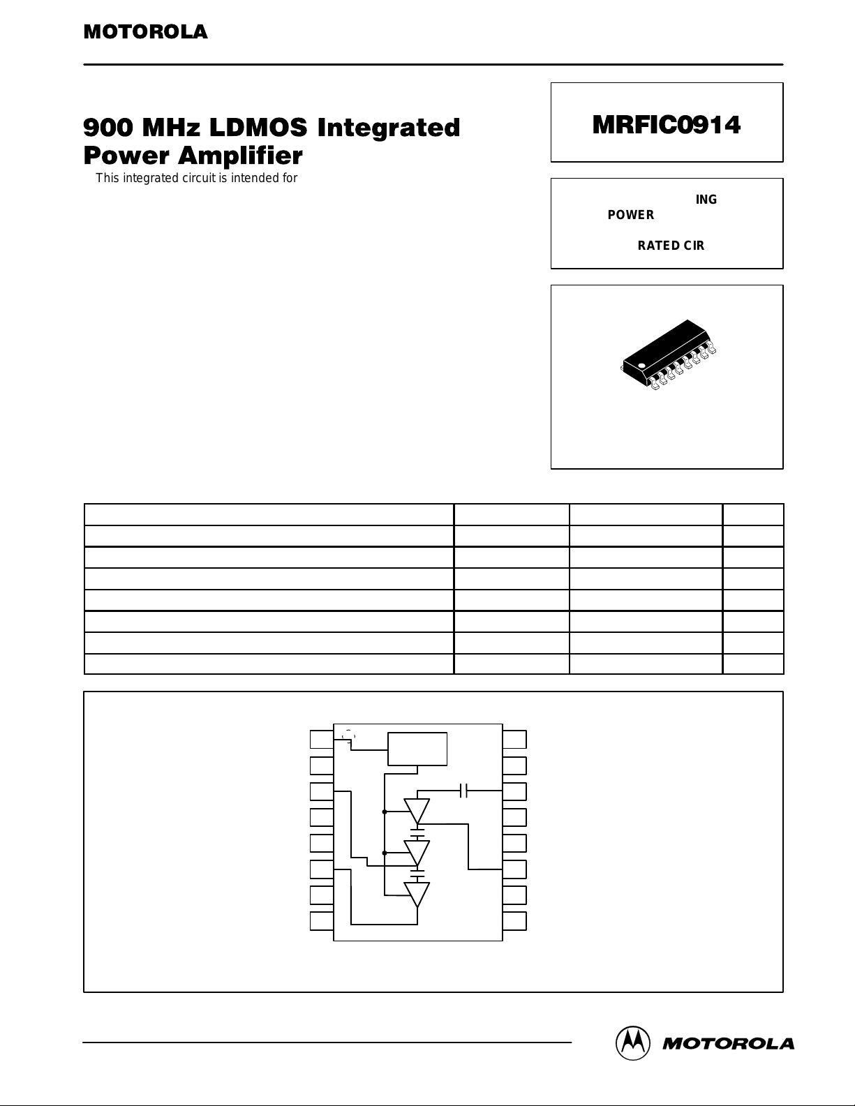
This integrated circuit is intended for two–way paging applications and for
other Industrial, Scientific and Medical (ISM) at 900 MHz band applications.
The three stage design is implemented in Motorola’s low cost, high performance LDMOS process and housed in a low–cost surface mount SOIC
package. Input and output matching is implemented off–chip for maximum
flexibility while interstage matching is on–chip. A power control pin is included
allowing 60 dB dynamic range.
• 30.5 dBm Output Power for 3 dBm Input Power at 900 MHz
• 32 dB Typ Small Signal Gain
• 40% Efficiency Min at 30.5 dBm Output Power
• 4.0 to 5.5 Volt Operation
• Low–Cost, Low Profile Plastic SOIC Package
• Order MRFIC0914R2 for Tape and Reel.
R2 Suffix = 2,500 Units per 16 mm, 13 inch Reel.
• Device Marking = M0914
ABSOLUTE MAXIMUM RATINGS
Supply Voltage V
Supply Current I
Power Control Voltage V
Input Power P
Ambient Operating Temperature T
Storage Temperature T
Thermal Resistance, Junction to Case θ
(TA = 25°C unless otherwise noted)
Rating
Symbol Value Unit
D1, VD2, VD3
Dtotal
CNTRL
stg
JC
900 MHz PAGING
POWER AMPLIFIER
Si MONOLITHIC
INTEGRATED CIRCUIT
CASE 751B–05
(SOIC–16)
9 Vdc
2 Adc
4.8 Vdc
in
A
6 dBm
–30 to +80 °C
–65 to +150 °C
26 °C/W
REV 2
Motorola, Inc. 1997
V
CNTRL
GND
V
GND
GND
RF OUT/V
GND
GND
D2
D3
1
2
3
4
5
6
7
8
CONTROL
16
15
14
13
12
11
10
GND
GND
RF IN
GND
GND
V
D1
GND
9
GND
Pin Connections and Functional Block Diagram
MRFIC0914MOTOROLA RF DEVICE DATA
1

RECOMMENDED OPERATING RANGES
Parameter Symbol Value Unit
Supply Voltage VD1, VD2,
Power Control Voltage V
RF Frequency Range f
V
CNTRL
RF
3.6 to 5.8 Vdc
D3
0 to 4.8 Vdc
890 to 928 MHz
ELECTRICAL CHARACTERISTICS (V
I
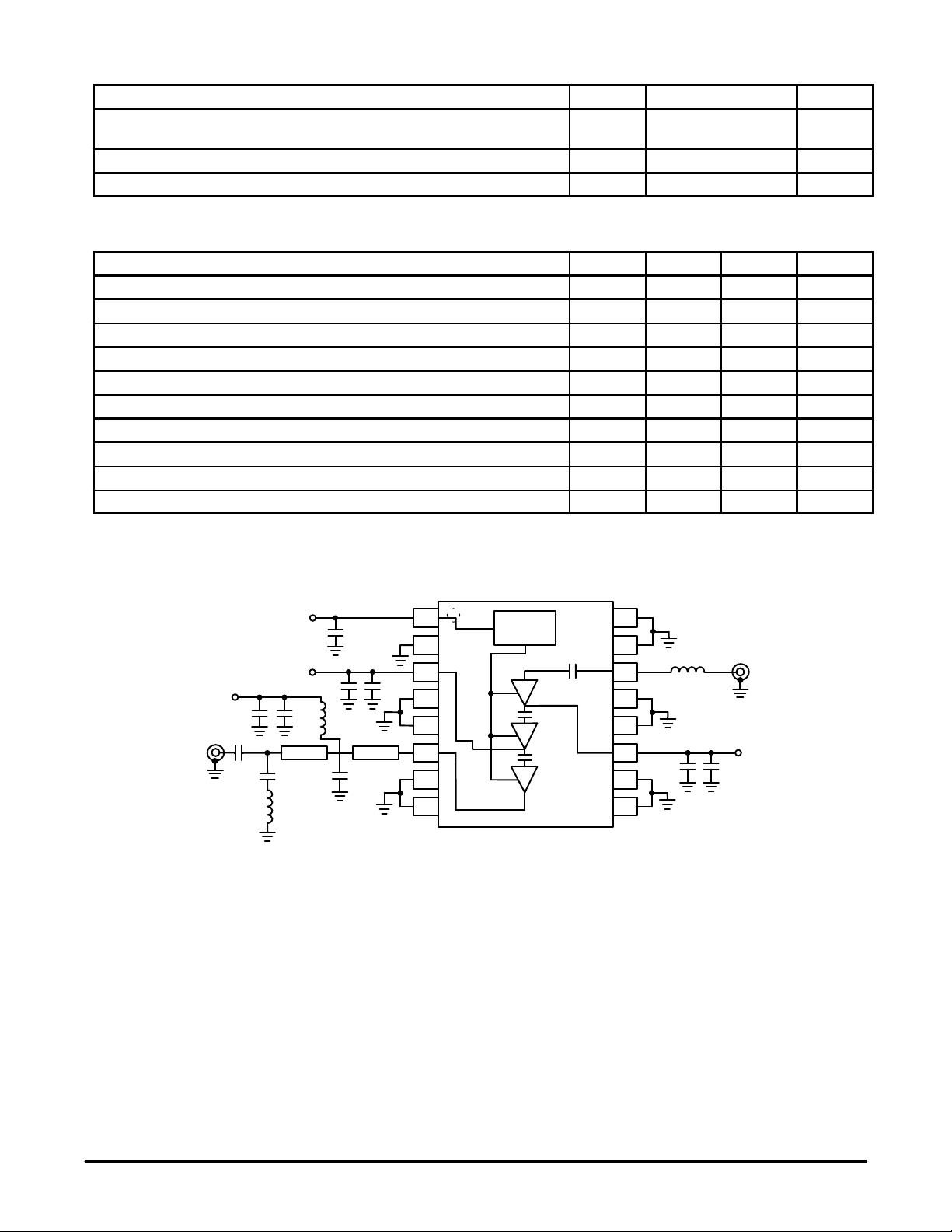
= 583 mA, TA = 25°C unless otherwise noted. Measured in Circuit Configuration Shown in Figure 1.)
Dtotal
Characteristic
Output Power 1.12 — — W
Efficiency 40 — — %
Output Power at 1 dB Gain Compression — 29 — dBm
Saturated Output Power — 31 — dBm
Output Third Order Intercept Point — 36 — dBm
Dynamic Range (V
Input Return Loss 7 12 — dB
Output Power, Low Voltage (VD1, VD2, VD3 = 3.84 V) 0.56 — — W
Spurious Output (Load VSWR = 20:1, All Phase Angles) — –60 –50 dBc
Harmonic Output (With External Matching Circuit) — — –45 dBc
RF OUT
= 0 to 4.8 V) — 60 — dB
CNTRL
V
CNTRL
V
D2
V
D3
C1
C10
C9
C2
, VD2, VD3 = 4.8 V, f = 900 MHz, Pin = 3 dBm, 1 ms, 10% duty cycle, V
D1
Min Typ Max Unit
C8
C4
1
2
3
C5
4
L
1
T1T2
C3
5
6
7
CONTROL
16
15
14
13
12
11
10
C6
L2
C7
CNTRL
RF INPUT
V
D3
Adjusted for
MRFIC0914
2
L
3
µ
C1, C7 — 0.01
C2, C6, C8 — 33 pF
C3 — 12 pF
C4 — 1.0
f
µ
F
8
C5, C10 — 100 pF
C9 — 2.1 pF
L1 — 33 nH
L2 — 5.6 nH
L3 — 3.3 nH
Ω
T1 — 50
T2 — 50
BOARD MATERIAL — 18 MIL FR4
MICROSTRIP, 7.5° @ 900 MHz
Ω
MICROSTRIP, 31.6° @ 900 MHz
Figure 1. Application Circuit Configuration
9
MOTOROLA RF DEVICE DATA
 Loading...