

SEMICONDUCTOR TECHNICAL DATA
The MRFIC Line
The MRFIC0903 is an integrated GaAs SPDT switch designed for
transceivers operating in the 100 MHz to 2.0 GHz frequency range. The design
utilizes Motorola’s advanced GaAs RF process to yield superior performance in
a cost effective monolithic device. Applications for the MRFIC0903 include
Class 4 and 5 GSM, Class 1 and 2 DCS1800, DCS1900, DAMPS, PDC, digital
cellular systems as well as analog cellular systems.
• 2.8 W Transmitting Capability through the T ransmit Path with a 5.0 Volt
Differential Control Signal
• 1.25 W Transmitting Capability through the T ransmit Path with a 3.0 Volt
Differential Control Signal
• Single Source Operating Supply Voltage
• Low Power Consumption
• Low–Cost, Low Profile Plastic SOIC Package
• Available in Tape and Reel by Adding R2 Suffix.
R2 Suffix = 2,500 Units per Reel.
• Device Marking = M0903
Order this document
by MRFIC0903/D
ANTENNA SWITCH
GaAs MONOLITHIC
INTEGRATED CIRCUIT
CASE 751–05
(SO–8)
ABSOLUTE MAXIMUM RATINGS (T
Rating Symbol Value Unit
Supply Voltage V
Control Voltage VC1, V
Power Dissipation P
Power Input (Non–selected Port) P
Ambient Operating Temperature T
Storage Temperature T
= 25°C unless otherwise noted)
A
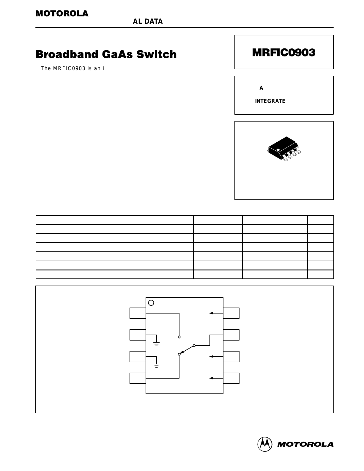
RF2
1
GND
2
GND
3
RF1
4
DD
D
in
A
stg
C2
10 Vdc
VDD + 0.8, VDD – 12 Vdc
1.0 W
0.325 W
–35 to +85 °C
–65 to +150 °C
V
8
C2
RFC
7
V
6
DD
V
5
C1
REV 1
Motorola, Inc. 1997
Pin Connections and Functional Block Diagram
MRFIC0903MOTOROLA RF DEVICE DATA
1
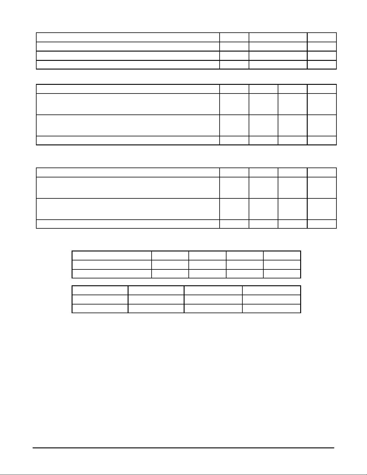
RECOMMENDED OPERATING RANGES
Parameter Symbol Value Unit
Supply Voltage V
Control Voltage Range VC1, V
RF Frequency Range f
DD
C2VDD
RF
0 to 5.0 Vdc
– 5.0 to VDD + 0.5 Vdc
100 to 2000 MHz
ELECTRICAL CHARACTERISTICS (V
Characteristic Min Typ Max Unit
Supply Current
I
DD
I
Control
VSWR
Insertion Loss (RFC/RF1, RFC/RF2)
Isolation (RFC/RF2, RFC/RF1)
Output Power at 0.1 dB Compression — 34.5 — dBm
Electrical Characteristics at 900 MHz measured in test circuit schematic shown in Figure 1 with board losses removed.
ELECTRICAL CHARACTERISTICS (V
Characteristic Min Typ Max Unit
Supply Current
I
DD
I
Control
VSWR
Insertion Loss (RFC/RF1, RFC/RF2)
Isolation (RFC/RF2, RFC/RF1)
Output Power at 0.1 dB Compression — 34 — dBm
Electrical Characteristics at 1800 MHz measured in test circuit schematic shown in Figure 2 with board losses removed.
= 5.0 V, Pin = 2.5 W (34 dBm), f = 900 MHz, TA = 25°C unless otherwise noted)
DD
—
—
—
—
18
= 5.0 V, Pin = 2.0 W (33 dBm), f = 1800 MHz, TA = 25°C unless otherwise noted)
DD
—
—
—
—
18
100
150
1.5:1
0.55
20
100
150
1.5:1
0.7
20
170
300
—
0.8
—
170
300
—
0.85
—
µA
µA
dB
dB
µA
µA
dB
dB
VC1 and VC2 Input Voltage
High V
Low VDD – 10 — VDD – 5 Vdc
V
C1
High Low Insertion Loss Isolation
Low High Isolation Insertion Loss
Min Typ Max Unit
DD
V
C2
— VDD + 0.5 Vdc
RFC – RF1 RFC – RF2
T able 1. Logic Levels
MRFIC0903
2
MOTOROLA RF DEVICE DATA
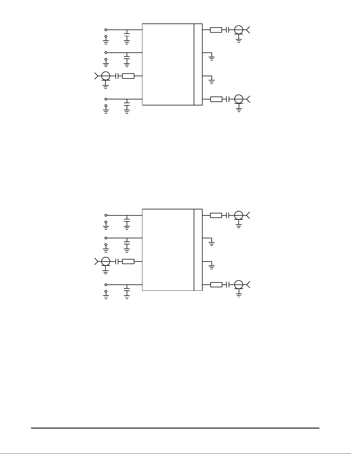
RF1
50
Ω
+
V
C1
–
C1
5
4
TL1 C2
+
V
DD
–
RFC
Ω
50
V
C2
C1, C5 — 2.7 pF, Chip Capacitor
C2, C4, C6 — 100 pF , Chip Capacitor
C3 — 10 pF, Chip Capacitor
Note: Decoupling capacitors on pins 5, 6 and 8 must be as close as possible to the pins.
C4 TL2
+
–
C3
C5
6
DUT
7
8
3
2
1
TL3 C6
TL1, TL3 — 12 degrees of 50 Ω line at 1 GHz
TL2 — 15 degrees of 50 Ω line at 1 GHz
Figure 1. 300 MHz to 1600 MHz Test Circuit Configuration
+
V
C1
–
C1
5
4
TL1 C2
RF2
50
RF1
50
Ω
Ω
+
V
DD
–
RFC
Ω
50
V
C2
C1, C5 — 1.3 pF, Chip Capacitor
C2, C3, C4, C6 — 8.2 pF , Chip Capacitor
Note: Decoupling capacitors on pins 5, 6 and 8 must be as close as possible to the pins.
C4 TL2
+
–
C3
C5
6
DUT
7
8
3
2
1
TL3 C6
TL1, TL3 — 12 degrees of 50 Ω line at 1 GHz
TL2 — 15 degrees of 50 Ω line at 1 GHz
Figure 2. 1600 MHz to 2000 MHz T est Circuit Configuration
RF2
50
Ω
MRFIC0903MOTOROLA RF DEVICE DATA
3
 Loading...