Motorola MRFIC0001 Datasheet

SEMICONDUCTOR TECHNICAL DATA
Order this document
by MRFIC0001/D
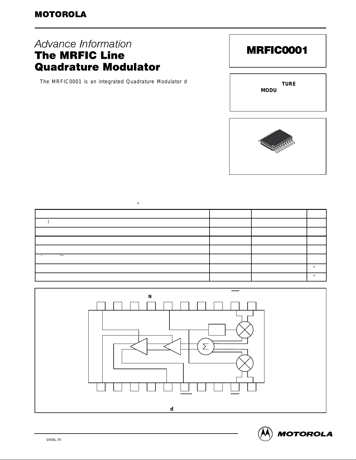
The MRFIC0001 is an integrated Quadrature Modulator designed for
operation in the 50 to 260 MHz frequency range. The design utilizes Motorola’s
advanced MOSAIC 3 silicon bipolar RF process to yield superior performance
in a cost effective monolithic device. Applications include DQPSK for PDC,
QUADRATURE
MODULAT OR
INTEGRATED CIRCUIT
NADC, and PHS; GMSK for GSM and DCS1800; and QPSK for CATV.
• Linear I/Q Ports
• On Chip LO Phase Shifter
• I/Q Phase Imbalance = 2 degrees (Typ)
• I/Q Amplitude Imbalance = 0.3 dB (Typ)
• Gain Control = 30 dB (Typ)
• Single Source Low Operating Supply Voltage
• Low Power Consumption
• Low–Cost, Low Profile Plastic TSSOP Package
CASE 948D–03
(TSSOP–20)
• Order MRFIC0001R2 for Tape and Reel.
R2 Suffix = 2,500 Units per 16 mm, 13 inch Reel.
• Device Marking = M001
ABSOLUTE MAXIMUM RATINGS (TA = 25_C unless otherwise noted)
Parameter Symbol Value Unit
Supply Voltage V
Control Voltages TX EN, VCNTL 6.5 Vdc
LO Input Power P
Differential I/Q Input Voltage V
I, I, Q, and Q DC Bias Voltage V
Ambient Operating Temperature T
Storage Temperature T
CC
LO
D
B
A
stg
6.5 Vdc
0.0 dBm
2.0 V
2.0 Vdc
–30 to +85
–65 to +125
pp
_
C
_
C
TX EN
20
1234567 9108
VCNTL
VCC GND
GND
19 18 17
GND VCC GND GNDOUT GND
LO
16
VGA
VCCGND GND
15 14 13 12 11
90
OUT I I
Q
Q
Pin Connections and Functional Block Diagram
This document contains information on a new product. Specifications and information herein are subject to change without notice.
REV 4
Motorola, Inc. 1997
MRFIC0001MOTOROLA RF DEVICE DATA
1

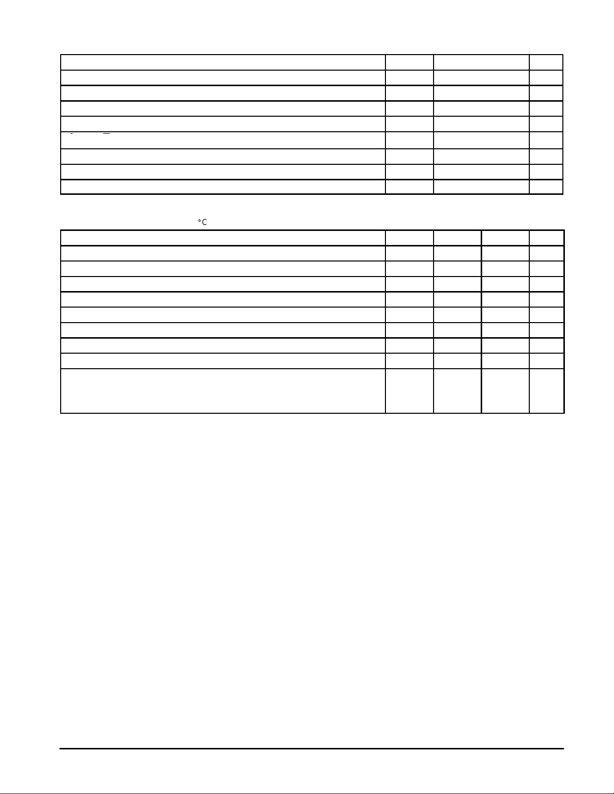
RECOMMENDED OPERATING CONDITIONS
Parameter Symbol Value Unit
Supply Voltage V
LO Input Power P
LO Frequency f
Differential I/Q Input Voltage V
I, I, Q, and Q DC Bias Voltage V
Variable Gain Amplifier Control Voltage V
Transmit Enable Low V oltage TX EN 0 to 0.2 Vdc
Transmit Enable High V oltage TX EN VCC – 0.2 to V
CC
LO
LO
D
B
cntl
2.7 to 5.5 Vdc
–10 dBm
50 to 260 MHz
0 to 1.0 Vdc
1.5 to 1.7 Vdc
0 to V
CC
CC
Vdc
Vdc
ELECTRICAL CHARACTERISTICS (V
fLO = 248 MHz, fD = 100 kHz, TA = 25_C unless otherwise noted)
Characteristic Min Typ Max Unit
Supply Current – 10 12 mA
Standby Current (TX EN = 0.0V) – 40 100 µA
Single Sideband Output Power Level –15 –13 – dBm
Single Sideband Output Power 1dB Compression Point – –10 – dBm
LO Leakage
Undesired Sideband Level – –35 –30 dBc
Output Level Dynamic Range (V
Turn–on/off Time – 2 – µs
I/Q Data
Input 3dB Bandwidth
Amplitude Imbalance
Phase Imbalance
(1) All electrical characteristics measured in test circuit schematic shown in Figure 1.
VB is the bias voltage on the input data ports.
VD is the sinusoidal differential voltage on the input data ports when testing the part in a single sideband mode.
Above power levels are the single–ended output power.
(2) LO leakage power is unaffected by V
(2)
= 0 to 2.2V)
cntl
= 3.0 V, TX EN = 3.0 V, V
CC
(2)
setting.
cntl
= 0.0 V, VD = 0.8 VPP, VB = 1.6 V, PLO = –10 dBm,
cntl
– –55 –45 dBm
– 30 – dB
–
–
–
5
0.3
2
–
–
–
MHz
degree
dB
EVALUATION BOARDS
Evaluation boards are available for RF Monolithic Integrated Circuits by adding a “TF” suffix to the device type. For a
complete list of currently available boards and ones in development for newly introduced product, please contact your
local Motorola Distributor or Sales Office.
MRFIC0001
MOTOROLA RF DEVICE DATA
2
 Loading...