

Motorola MRF897R Datasheet
1
MRF897RMOTOROLA RF DEVICE DATA
The RF Line
Designed for 24 Volt UHF large–signal, common emitter, class–AB linear
amplifier applications in industrial and commercial FM/AM equipment operating
in the range 800–970 MHz.
• Specified 24 Volt, 900 MHz Characteristics
Output Power = 30 Watts
Minimum Gain = 10.5 dB @ 900 MHz, class–AB
Minimum Efficiency = 30% @ 900 MHz, 30 Watts (PEP)
Maximum Intermodulation Distortion –30 dBc @ 30 Watts (PEP)
• Characterized with Series Equivalent Large–Signal Parameters from 800
to 960 MHz
• Silicon Nitride Passivated
• 100% Tested for Load Mismatch Stress at all Phase Angles with 5:1 VSWR
@ 26 Vdc, and Rated Output Power
• Gold Metalized, Emitter Ballasted for Long Life and Resistance to Metal–
Migration
• Circuit Board Photomaster Available by Ordering Document
MRF897RPHT/D from Motorola Literature Distribution.
MAXIMUM RATINGS
Rating Symbol Value Unit
Collector–Emitter Voltage V
CEO
30 Vdc
Collector–Emitter Voltage V
CES
60 Vdc
Emitter–Base Voltage V
EBO
4.0 Vdc
Collector–Current — Continuous I
C
4.0 Adc
Total Device Dissipation @ TC = 25°C
Derate above 25°C
P
D
105
0.60
Watts
W/°C
Storage Temperature Range T
stg
–65 to +150 °C
THERMAL CHARACTERISTICS
Characteristic Symbol Max Unit
Thermal Resistance, Junction to Case R
θJC
1.67 °C/W
ELECTRICAL CHARACTERISTICS (T
C
= 25°C unless otherwise noted)
Characteristic
Symbol Min Typ Max Unit
OFF CHARACTERISTICS
Collector–Emitter Breakdown Voltage (IC = 50 mAdc, IB = 0) V
(BR)CEO
30 33 — Vdc
Collector–Emitter Breakdown Voltage (IC = 50 mAdc, VBE = 0) V
(BR)CES
60 80 — Vdc
Emitter–Base Breakdown Voltage (IE = 5 mAdc, IC = 0) V
(BR)EBO
4.0 4.7 — Vdc
Collector Cutoff Current (VCE = 30 Vdc, VBE = 0, TC = 25°C) I
CES
— — 10.0 mAdc
ON CHARACTERISTICS
DC Current Gain (ICE = 1.0 Adc, VCE = 5 Vdc) h
FE
30 80 120 —
DYNAMIC CHARACTERISTICS
Output Capacitance (VCB = 24 Vdc, IE = 0, f = 1.0 MHz) C
ob
14 21 28 pF
(continued)
Order this document
by MRF897R/D
SEMICONDUCTOR TECHNICAL DATA
30 W, 900 MHz
RF POWER
TRANSISTOR
NPN SILICON
CASE 395B–01, STYLE 1
Motorola, Inc. 1995
MRF897R
2
MOTOROLA RF DEVICE DATA
ELECTRICAL CHARACTERISTICS — continued (T
C
= 25°C unless otherwise noted)
Characteristic
Symbol Min Typ Max Unit
FUNCTIONAL CHARACTERISTICS
Common–Emitter Amplifier Power Gain
(VCC = 24 Vdc, P
out
= 30 Watts (PEP), Icq = 125 mA, f1 = 900 MHz,
f2 = 900.1 MHz)
G
pe
10.5 12.0 — dB
Collector Efficiency
(VCC = 24 Vdc, P
out
= 30 Watts (PEP), Icq = 125 mA, f1 = 900 MHz,
f2 = 900.1 MHz)
η 30 38 — %
Intermodulation Distortion
(VCC = 24 Vdc, P
out
= 30 Watts (PEP), Icq = 125 mA, f1 = 900 MHz,
f2 = 900.1 MHz)
IMD — –37 –30 dBc
Output Mismatch Stress
(VCC = 26 Vdc, P
out
= 30 Watts (PEP), Icq = 125 mA, f1 = 900 MHz,
f2 = 900.1 MHz, Load VSWR = 5:1 (all phase angles))
ψ No Degradation in Output Power
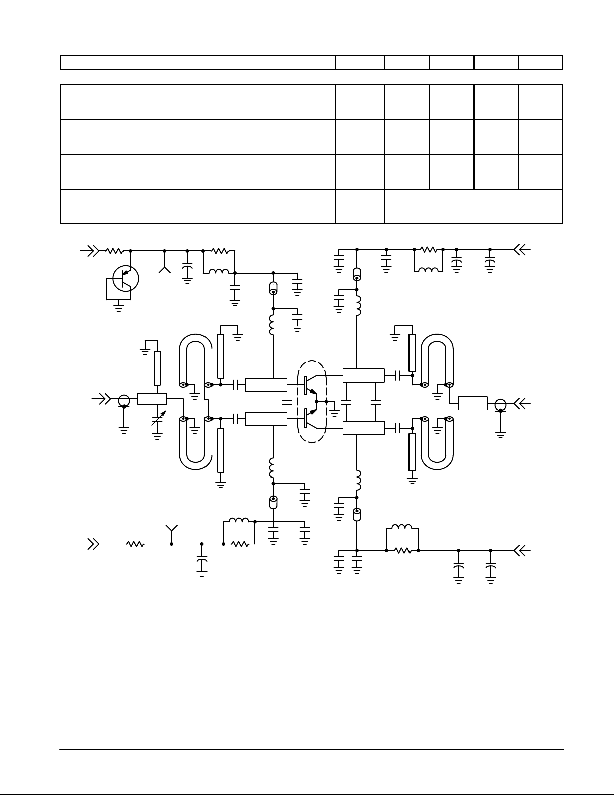
COAX 1
BALUN 1
INPUT
TL2
TL1
C1
C2
C3
TL4
TL3
TL5
TL6
C10
DUT
R3
B1
TL7
TL8
C15
C20
C23
C24
C4
C25
L3
C6
+
V
B
R1
V
BB
Q1
C8
TL11
OUTPUT
COAX 2
BALUN 2
TL9
TL10
B3
C16
L7
C21
C18
V
CC
R5
L5
C11
+
C13
+
C9
L1
L2
B2
L4
R4
C5C26
C7
+
V
B
R2
V
BB
L8
C17
B4
C22 C19
L6
R6
C12+C14
+
V
CC
B1, B2, B3, B4 — Short Ferrite Bead, Fair Rite #2743019447
C1 — 0.8–8.0 pF Var Capacitor, Johansen Gigatrim
C2, C3, C23, C24 — 43 pF, 100 mil, ATC Chip Capacitor
C4, C5, C21, C22 — 1000 pF, 100 mil, ATC Chip Capacitor
C6, C7, C11, C12 — 10 µF, Electrolytic Capacitor, Panasonic
C8, C9, C16, C17 — 100 pF, 100 mil, ATC Chip Capacitor
C10 — 9.1 pF, 50 mil, ATC Chip Capacitor
C13 — 250 µF Electrolytic Capacitor, Mallory
C14, C18, C19, C25 — 0.1 µF, Chip Capacitor, Kemet
C15 — 1.1 pF, 50 mil, ATC Chip Capacitor
C20 — 6.8 pF, 100 mil, ATC Chip Capacitor
L1, L2, L3, L4, L5, L6, L7, L8 — 5 Turns 20 AWG,
IDIA 0.126″ Choke, Taylor Spring 46 nH
Figure 1. 840–900 MHz Test Circuit Schematic
N1, N2 — Type N Flange Mount, Omni Spectra 3052–1648–10
Q1 — Bias Transistor BD136 PNP
R1, R12 — 27 Ohm, 2.0 W
R3, R4, R5, R6 — 4.0 x 39 Ohm, 1/8 W, Chips Resistors in
R3, R4, R5, R6 — Parallel, Rohm 390–J
SB1 — 0.15″ x 0.3″ x 0.03″ Cu
TL1–TL11 — Microstrip Line, See Photomaster
Balun1, Balun2, Coax 1, Coax 2 — 2.20″ 50 Ohm, 0.086″ o.d.
Balun1, Balun2, Coax 1, Coax 2 — semi–rigid coax, Micro Coax
Balun1, Balun2, Coax 1, Coax 2 — UT–85–M17
Circuit Board — 1/32″ Glass Teflon, Arlon GX–0300–55–22,
Circuit Board — εr = 2.55
 Loading...