

Motorola MRF891S, MRF891 Datasheet

2–11
MRF891 MRF891SMOTOROLA RF DEVICE DATA
The RF Line
. . . designed for 24 volt UHF large–signal, common–emitter amplifier applications in industrial and commercial FM e quipment operating in the range of
800–960 MHz.
• Specified 24 Volt, 900 MHz Characteristics
Output Power = 5.0 Watts
Power Gain = 9.0 dB Min
Efficiency = 50% Min
• Series Equivalent Large–Signal Characterization
• Capable of Withstanding 20:1 VSWR Load Mismatch at Rated Output
Power and Supply Voltage
• Gold Metallized, Emitter Ballasted for Long Life and Resistance to Metal
Migration
• Silicon Nitride Passivated
• Circuit board photomaster available upon request by contacting
RF Tactical Marketing in Phoenix, AZ.
MAXIMUM RATINGS
Rating Symbol Value Unit
Collector–Emitter Voltage V
CEO
30 Vdc
Collector–Emitter Voltage V
CES
55 Vdc
Emitter–Base Voltage V
EBO
4.0 Vdc
Collector Current — Continuous I
C
0.6 Adc
Total Device Dissipation @ TA = 50°C (1)
Derate above 50°C
P
D
18
0.143
Watts
W/°C
Storage Temperature Range T
stg
–65 to +150 °C
THERMAL CHARACTERISTICS
Characteristic Symbol Max Unit
Thermal Resistance, Junction to Case (2) R
θJC
7.0 °C/W
ELECTRICAL CHARACTERISTICS (T
C
= 25°C unless otherwise noted.)
Characteristic
Symbol Min Typ Max Unit
OFF CHARACTERISTICS
Collector–Emitter Breakdown Voltage
(IC = 20 mAdc, IB = 0)
V
(BR)CEO
30 — — Vdc
Collector–Emitter Breakdown Voltage
(IC = 20 mAdc, VBE = 0)
V
(BR)CES
55 — — Vdc
Emitter–Base Breakdown Voltage
(IE = 0.5 mAdc, IC = 0)
V
(BR)EBO
4.0 — — Vdc
Collector Cutoff Current
(VCE = 30 Vdc, VBE = 0, TC = 25°C)
I
CES
— — 1.0 mAdc
ON CHARACTERISTICS
DC Current Gain
(IC = 200 mAdc, VCE = 5.0 Vdc)
h
FE
30 — 150 —
NOTES: (continued)
1. This device is designed for RF operation. The total device dissipation rating applies only when the device is operated as an RF amplifier.
2. Thermal Resistance is determined under specified RF operating conditions by infrared measurement techniques.
Order this document
by MRF891/D
SEMICONDUCTOR TECHNICAL DATA
5.0 W, 900 MHz
RF POWER
TRANSISTORS
NPN SILICON
CASE 319–07, STYLE 2
MRF891
CASE 319A–02, STYLE 2
MRF891S
Motorola, Inc. 1994
REV 6
MRF891 MRF891S
2–12
MOTOROLA RF DEVICE DATA
ELECTRICAL CHARACTERISTICS — continued (T
C
= 25°C unless otherwise noted.)
Characteristic
Symbol Min Typ Max Unit
DYNAMIC CHARACTERISTICS
Output Capacitance
(VCB = 24 Vdc, IE = 0, f = 1.0 MHz)
C
ob
— 6.5 8.0 pF
FUNCTIONAL TESTS
Common–Emitter Amplifier Power Gain (Broadband)
(VCC = 24 Vdc, P
out
= 5.0 W, f = 900 MHz)
G
pe
9.0 10 — dB
Collector Efficiency
(VCC = 24 Vdc, P
out
= 5.0 W, f = 900 MHz)
η 50 57 — %
Load Mismatch Stress
(VCC = 24 Vdc, Pin = 0.63 W, f = 900 MHz,
VSWR = 20:1, all phase angles)
ψ
No Degradation in Output Power
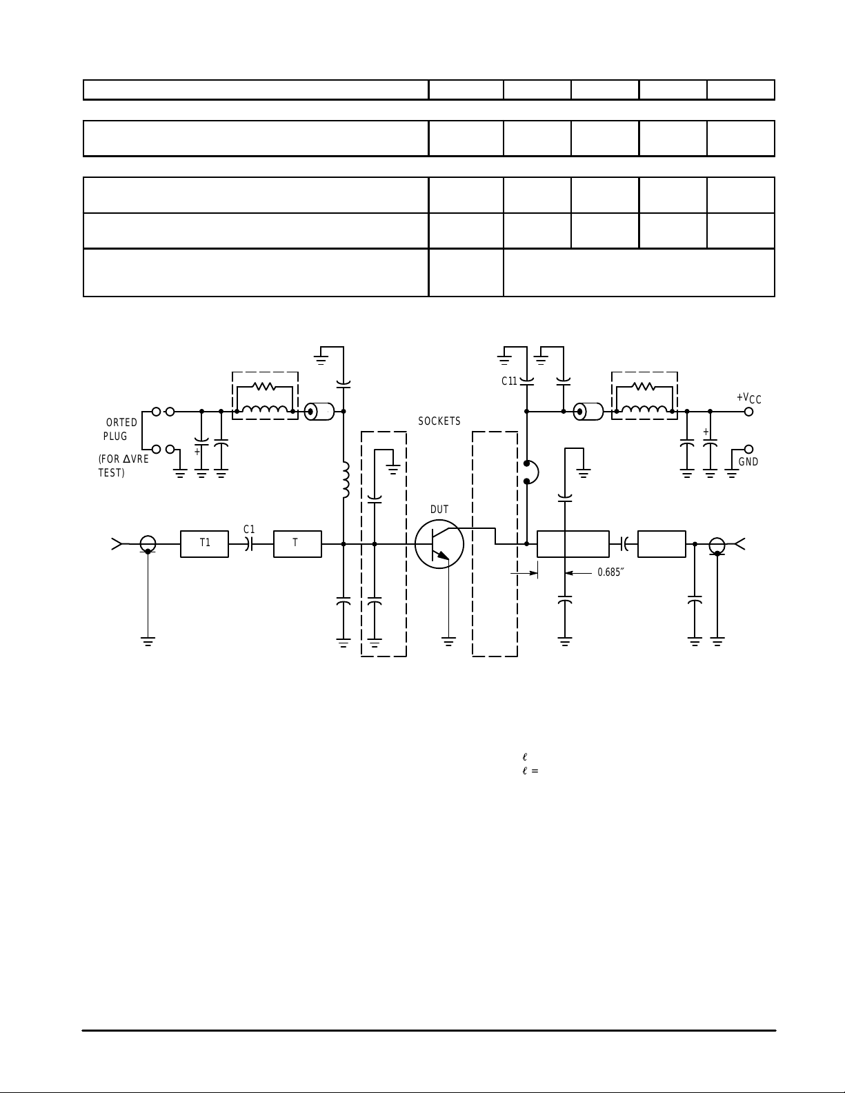
Figure 1. Broadband Test Fixture
C1 — 39 pF, 100 Mil Chip Capacitor
C2, C8, C15 — 0.8–8.0 pF Johansen Gigatrim
C3, C4 — 12 pF, Mini–Unelco
C5, C13 — 1000 pF, 350 V Unelco
C6, C14 — 10 µF, 25 V Tantalum
C7, C11, C12 — 91 pF, Mini–Unelco
C9 — 5.0 pF, MIni–Unelco
C10 — 47 pF, 100 Mil Chip Capacitor
L1, L6 — 10 Turns #20 AWG Around 10 Ohm 1/2 Watt Resistor
L2, L5 — Ferrite Bead
L3 — 4 Turns #16 AWG Choke
L4 — 0.5″, #18 AWG Wire
T1, T4 — 50 Ohm Microstrip Line
T2 — W = 165 Mils, ȏ = 1946 Mils
T3 — W = 166 Mils, ȏ = 1563 Mils
PC Board — 0.031″ Glass Teflon (εr = 2.56)
SHORTED
PLUG
(FOR
∆
VRE
TEST)
+V
CC
GND
0.685
″
DUT
SOCKETS
+
+
C1
C11
T1 T2 T3 T4
C6 C5
L1
L2
C7
L3
C2
C4
C3 C9
L5
L6
C12
C13 C14
C15
C10
C8
L4
 Loading...