

Motorola MRF842 Datasheet

1
MRF842MOTOROLA RF DEVICE DATA
The RF Line
. . . designed for 12.5 volt UHF large–signal, common–base amplifier applications in industrial and commercial FM e quipment operating in the range of
806–960 MHz.
• Specified 12.5 Volt, 870 MHz Characteristics
Output Power = 20 Watts
Power Gain = 6.0 dB Min
Efficiency = 50% Min
• Series Equivalent Large–Signal Characterization
• Internally Matched Input for Broadband Operation
• 100% Tested for Load Mismatch Stress at All Phase Angles with 20:1
VSWR @ 15.5 Volt Supply and 50% RF Overdrive
• Gold Metallized, Emitter Ballasted for Long Life and Resistance to Metal
Migration
• Silicon Nitride Passivated
MAXIMUM RATINGS
Rating Symbol Value Unit
Collector–Emitter Voltage V
CEO
16 Vdc
Collector–Base Voltage V
CBO
36 Vdc
Emitter–Base Voltage V
EBO
4.0 Vdc
Collector Current — Continuous I
C
7.6 Adc
Total Device Dissipation @ TC = 25°C (1)
Derate above 25°C
P
D
80
0.64
Watts
W/°C
Storage Temperature Range T
stg
–65 to +150 °C
THERMAL CHARACTERISTICS
Characteristic Symbol Max Unit
Thermal Resistance, Junction to Case (2) R
θJC
1.5 °C/W
ELECTRICAL CHARACTERISTICS (T
C
= 25°C unless otherwise noted.)
Characteristic
Symbol Min Typ Max Unit
OFF CHARACTERISTICS
Collector–Emitter Breakdown Voltage
(IC = 50 mAdc, IB = 0)
V
(BR)CEO
16 — — Vdc
Collector–Emitter Breakdown Voltage
(IC = 50 mAdc, VBE = 0)
V
(BR)CES
36 — — Vdc
Emitter–Base Breakdown Voltage
(IE = 10 mAdc, IC = 0)
V
(BR)EBO
4.0 — — Vdc
Collector Cutoff Current
(VCB = 15 Vdc, IE = 0)
I
CBO
— — 5.0 mAdc
NOTES: (continued)
1. This device is designed for RF operation. The total device dissipation rating applies only when the device is operated as an RF amplifier.
2. Thermal Resistance is determined under specified RF operating conditions by infrared measurement techniques.
Order this document
by MRF842/D
SEMICONDUCTOR TECHNICAL DATA
20 W, 870 MHz
RF POWER
TRANSISTOR
NPN SILICON
CASE 319–07, STYLE 1
Motorola, Inc. 1994
REV 6
MRF842
2
MOTOROLA RF DEVICE DATA
ELECTRICAL CHARACTERISTICS — continued (T
C
= 25°C unless otherwise noted.)
Characteristic
Symbol Min Typ Max Unit
ON CHARACTERISTICS
DC Current Gain
(IC = 2.0 Adc, VCE = 5.0 Vdc)
h
FE
10 — — —
DYNAMIC CHARACTERISTICS
Output Capacitance
(VCB = 12.5 Vdc, IE = 0, f = 1.0 MHz)
C
ob
— 45 65 pF
FUNCTIONAL TESTS
Common–Base Amplifier Power Gain
(P
out
= 20 W, VCC = 12.5 Vdc, f = 870 MHz)
G
PB
6.0 7.0 — dB
Collector Efficiency
(P
out
= 20 W, VCC = 12.5 Vdc, f = 870 MHz)
η 50 55 — %
Load Mismatch Stress
(VCC = 15.5 Vdc, Pin (3) = 6.0 W, f = 870 MHz,
VSWR = 20:1, all phase angles)
—
No Degradation in Output Power
NOTE:
3. Pin = 150% of the typical input power requirement for 20 W output power @ 12.5 Vdc.
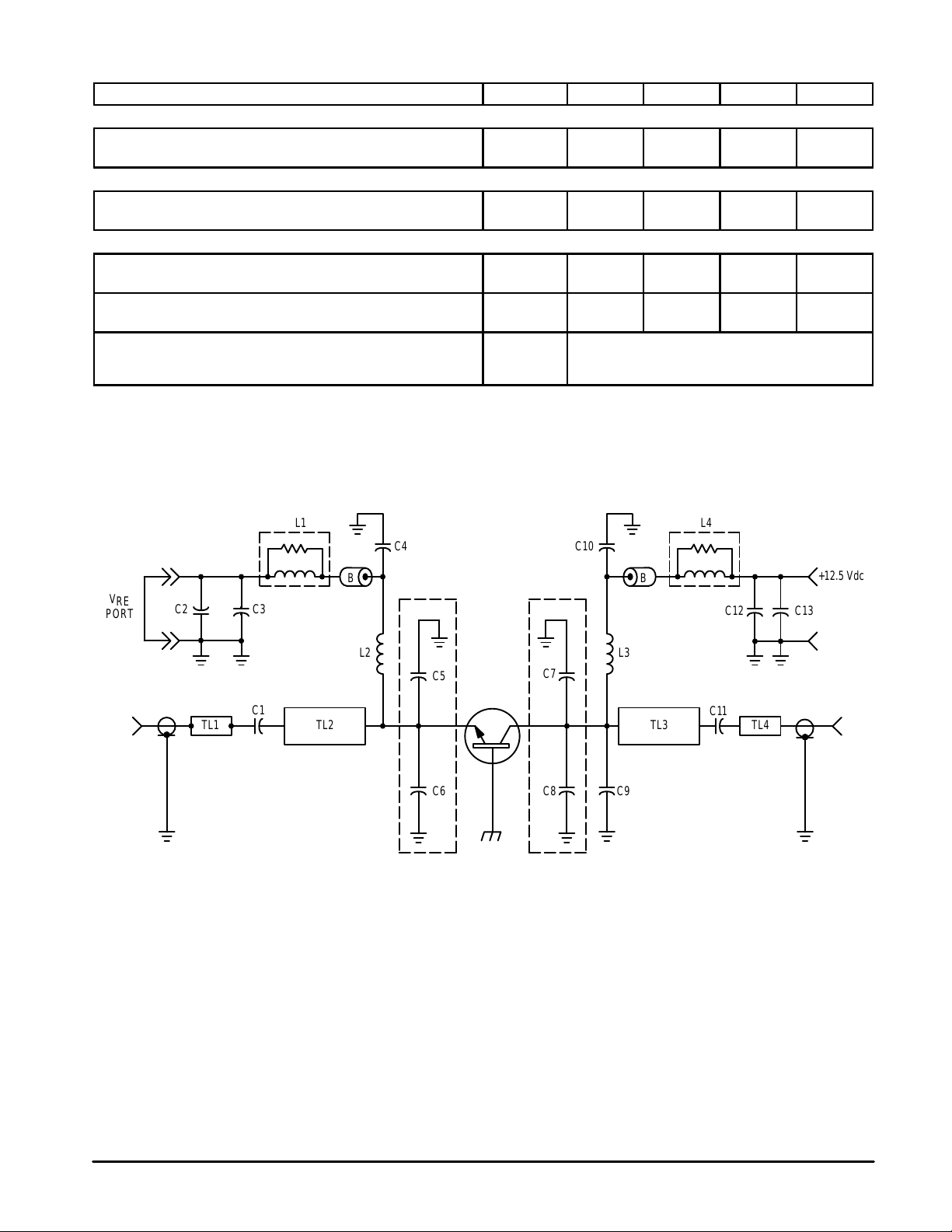
Figure 1. 870 MHz Test Circuit Schematic
B — Ferrite Bead, Ferroxcube 56–590–65–3B
C1, C11 — 51 pF, 100 Mil Chip Capacitor
C2, C13 — 15 µF, 20 WV Tantalum
C3, C12 — 1000 pF Unelco J101
C4, C10 — 91 pF Mini–Underwood
C5 — 15 pF Mini–Underwood
C6 — 12 pF Mini–Underwood
C7, C8 — 21 pF Mini–Underwood
C9 — 11 pF Mini–Underwood
L1, L4 — 11 Turns #20 AWG Over 10 ohm 1/2 W Carbon
L2, L3 — 4 Turns #20 AWG, 200 Mil ID
TL1, TL4 — Micro Strip, Zo = 50 Ω
TL2 — Micro Strip, Zo = 38 Ω, λ/4 @ 838 MHz
TL3 — Micro Strip, Zo = 24 Ω, λ/4 @ 838 MHz
Board — 0.032″ Glass Teflon
Board — 2 oz. Cu CLAD, εr = 2.55
C2
L4
C3
L1
L2
C12 C13
BB
C1
C11
TL4
C9C6
L3
C4 C10
TL3TL2TL1
+12.5 Vdc
V
RE
PORT
C5
C7
C8
D.U.T.
+
+
SOCKET SOCKET
 Loading...