

Motorola MRF2947RAT2, MRF2947RAT1, MRF2947AT2, MRF2947AT1 Datasheet
SEMICONDUCTOR TECHNICAL DATA
The RF Line
Order this document
by MRF2947/D
Motorola’s MRF2947 device contains two high performance, low–noise NPN
silicon bipolar transistors. This device has two 941 die housed in the high
performance six leaded SC–70ML package; yielding a 9 GHz current
gain–bandwidth product.
The RF performance at levels of 1 volt and 1 mA makes the MRF2947 well
suited for low–voltage, low–current, front–end applications such as paging,
cellular, GSM, DECT, CT2 and other portable wireless systems. The MRF2947
is fully ion–implanted with gold metallization and nitride passivation for
maximum device reliability , performance and uniformity.
• Low Noise Figure, NF = 1.5 dB (Typ) @ 1 GHz @ 5 mA
• High Current Gain–Bandwidth Product, ft = 9 GHz (Typ) @ 6 Volts, 15 mA
• Maximum Stable Gain, 18 dB @ 1 GHz @ 5 mA
• Output Third Order Intercept, OIP3 = +27 dBm
• Available in Tape and Reel Packaging Options:
T1 Suffix = 3,000 Units per 8 mm, 7 inch Reel
T2 Suffix = 3,000 Units per 8 mm, 7 inch Reel (reverse device
orientation in tape)
I
Cmax
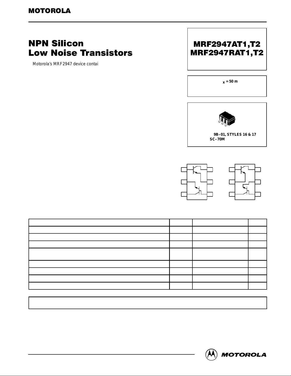
TRANSISTORS
CASE 419B–01, STYLES 16 & 17
SC–70ML/SOT–363
STYLE 16
B1 C1
E2
E1
= 50 mA
LOW NOISE
STYLE 17
B1 C1
E1
E2
MAXIMUM RATINGS
Rating Symbol Value Unit
Collector–Emitter Voltage V
Collector–Base Voltage V
Emitter–Base Voltage V
Power Dissipation (1) TC = 75°C
Derate linearly above TC = 75°C @
Collector Current — Continuous (2) I
Maximum Junction Temperature T
Storage Temperature T
Thermal Resistance, Junction to Case R
DEVICE MARKINGS
MRF2947AT1,T2 = WU
MRF2947RA T1,T2 = XR
(1) T o calculate the junction temperature use TJ = PD x R
body.
(2) IC — Continuous (MTBF > 10 years).
+ TC. The case temperature is measured on collector lead adjacent to the package
θJC
C2
MRF2947A T1,T2 MRF2947RA T1,T2
CEO
CBO
EBO
P
Dmax
C
Jmax
stg
θJC
B2
C2
10 Vdc
20 Vdc
1.5 Vdc
0.188
2.5
50 mA
150 °C
–55 to +150 °C
400 °C/W
B2
Watts
mW/°C
Motorola, Inc. 1997
MRF2947A T1,T2 MRF2947RAT1,T2MOTOROLA RF DEVICE DATA
1

ELECTRICAL CHARACTERISTICS (T
Characteristic Symbol Min Typ Max Unit
= 25°C unless otherwise noted)
A
OFF CHARACTERISTICS (3)
Collector–Emitter Breakdown V oltage
(IC = 0.1 mA, IB = 0)
Collector–Base Breakdown Voltage
(IC = 0.1 mA, IE = 0)
Emitter Cutoff Current
(VEB = 1 V, IC = 0)
Collector Cutoff Current
(VCB = 10 V, IE = 0)
V
(BR)CEO
V
(BR)CBO
I
EBO
I
CBO
ON CHARACTERISTICS (3)
DC Current Gain (VCE = 1 V, IC = 500 µA)
DC Current Gain (VCE = 6 V, IC = 5 mA)
h
FE
h
FE
DYNAMIC CHARACTERISTICS
Collector–Base Capacitance
(VCB = 1 V, IE = 0, f = 1 MHz)
Current Gain — Bandwidth Product
(VCE = 6 V, IC = 15 mA, f = 1 GHz)
C
cb
f
T
PERFORMANCE CHARACTERISTICS
Conditions Symbol Min Typ Max Unit
Insertion Gain
(VCE = 1 V, IC = 1 mA, f = 1 GHz)
(VCE = 6 V, IC = 15 mA, f = 1 GHz)
Maximum Unilateral Gain (4)
(VCE = 1 V, IC = 1 mA, f = 1 GHz)
(VCE = 6 V, IC = 15 mA, f = 1 GHz)
Maximum Stable Gain and/or Maximum Available Gain (5)
(VCE = 1 V, IC = 1 mA, f = 1 GHz)
(VCE = 6 V, IC = 15 mA, f = 1 GHz)
Noise Figure — Minimum
(VCE = 1 V, IC = 1 mA, f = 1 GHz)
(VCE = 6 V, IC = 5 mA, f = 1 GHz)
Noise Resistance
(VCE = 1 V, IC = 1 mA, f = 1 GHz)
(VCE = 6 V, IC = 5 mA, f = 1 GHz)
Associated Gain at Minimum NF
(VCE = 1 V, IC = 1 mA, f = 1 GHz)
(VCE = 6 V, IC = 5 mA, f = 1 GHz)
Output Power at 1 dB Gain Compression (6)
(VCE = 6 V, IC = 15 mA, f = 1 GHz)
Output Third Order Intercept (6)
(VCE = 6 V, IC = 15 mA, f = 1 GHz)
(3) Pulse width ≤ 300 µs, duty cycle ≤ 2% pulsed.
(4) Maximum unilateral gain is GU
(5) Maximum available gain and maximum stable gain are defined by the K factor as follows:
(6) ZO = 50 Ω and Z
matched for small signal maximum gain.
out
max
=
(1
–
|S11|2)(1–|S
2
|S
|
21
|2)
22
|S21|
G
Umax
MSG
MAG
NF
R
G
P
OIP
min
NF
1dB
1
3
N
3
2
MAG =
10 12 — Vdc
20 23 — Vdc
— — 0.1 µA
— — 0.1 µA
50 — — —
75 — 150 —
— 0.42 — pF
— 9 — GHz
—
—
—
—
—
—
—
—
—
—
—
—
— +13 — dBm
— +27 — dBm
|S
|
21
|S12|
|S
|
21
|S12|
7
15
13
17
12
18
1.8
1.5
22
17
9
14
2
"
K
(K
, if K < 1MSG =
–
1Ǹ)
—
—
—
—
—
—
—
—
—
—
—
—
, if K > 1
dB
dB
dB
dB
Ω
dB
MRF2947AT1,T2 MRF2947RAT1,T2
2
MOTOROLA RF DEVICE DATA

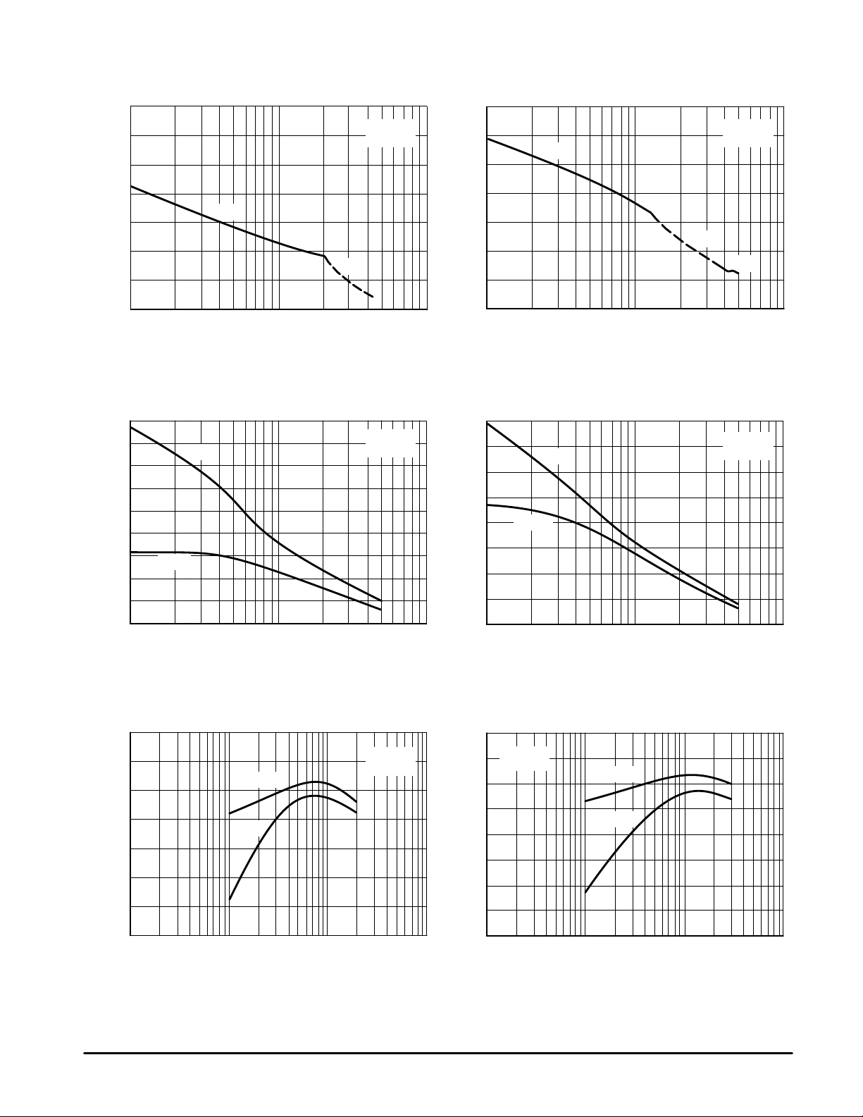
TYPICAL CHARACTERISTICS
1.4
1.2
1.0
0.8
0.6
0.4
C, CAPACITANCE (pF)
0.2
0
024 8106
C
ob
C
cb
VCB, REVERSE VOLTAGE (V)
Figure 1. Capacitance versus V oltage
180
160
140
120
100
80
, DC CURRENT GAIN
FE
60
h
40
20
0.1 1
IC, COLLECTOR CURRENT (mA)
10
f = 1 MHz
VCE = 1 V
100
1.6
1.4
1.2
1.0
C
0.8
0.6
, INPUT CAP ACITANCE
IB
0.4
C
0.2
0
0 0.4 0.8 1.41.2 1.61.0 1.8
Ib
0.2 0.6 2.0
VEB, EMITTER–BASE VOLTAGE (V)
Figure 2. Input Capacitance versus V oltage
10
VCE = 6 V
9
f = 1 GHz
8
7
6
5
4
3
, GAIN BANDWIDTH PRODUCT (GHz)
2
T
f
1
0.1 1 10010
IC, COLLECTOR CURRENT (mA)
f = 1 MHz
RF
INPUT
P
in
Figure 3. DC Current Gain versus
Collector Current
V
BE
BIAS NETWORK
*SLUG TUNER
Figure 5. Functional Circuit Schematic
DUT
Figure 4. Gain–Bandwidth Product versus
Collector Current
V
CE
RF
OUTPUT
*SLUG TUNER
BIAS NETWORK
*MICROLAB/FXR
SF–11N < 1 GHz
SF–31N > 1 GHz
P
MRF2947AT1,T2 MRF2947RAT1,T2MOTOROLA RF DEVICE DATA
out
3
TYPICAL CHARACTERISTICS
35
30
25
20
15
10
MAXIMUM AVAILABLE GAIN (dB)
MSG, MAXIMUM STABLE GAIN; MAG,
5
0
0.1 1 10
MSG
MAG
f, FREQUENCY (GHz)
Figure 6. Maximum Stable/Available Gain
versus Frequency
40
,
35
Umax
30
25
20
15
10
5
, FORWARD INSER TION GAIN; G
2
MAXIMUM UNILA TERAL GAIN (dB)
0
21
S
–5
0.1 1
S21
G
Umax
2
f, FREQUENCY (GHz)
VCE = 1 V
IC = 1 mA
VCE = 1 V
IC = 1 mA
35
30
25
20
15
10
MAXIMUM AVAILABLE GAIN (dB)
MSG, MAXIMUM STABLE GAIN; MAG,
40
,
35
Umax
30
25
20
15
10
, FORWARD INSER TION GAIN; G
2
MAXIMUM UNILA TERAL GAIN (dB)
21
S
10
VCE = 6 V
MSG
5
0
0.1 1
f, FREQUENCY (GHz)
IC = 5 mA
MAG
MSG
Figure 7. Maximum Stable/Available Gain
versus Frequency
VCE = 6 V
G
Umax
2
S21
5
0
0.1 1 10
f, FREQUENCY (GHz)
IC = 5 mA
10
Figure 8. Maximum Unilateral Gain and
Forward Insertion Gain versus Frequency
18
,
16
Umax
G
S21
Umax
2
10
14
12
10
8
, FORWARD INSER TION GAIN; G
6
2
MAXIMUM UNILA TERAL GAIN (dB)
21
S
4
0.1 1
IC, COLLECTOR CURRENT (mA)
Figure 10. Maximum Unilateral Gain and
Forward Insertion Gain versus Collector Current
MRF2947AT1,T2 MRF2947RAT1,T2
4
VCE = 1 V
f = 1 GHz
100
Figure 9. Maximum Unilateral Gain and
Forward Insertion Gain versus Frequency
20
,
VCE = 6 V
18
Umax
, FORWARD INSER TION GAIN; G
2
21
S
f = 1 GHz
16
14
12
10
8
MAXIMUM UNILA TERAL GAIN (dB)
6
4
0.1 1 10010
IC, COLLECTOR CURRENT (mA)
G
Umax
S21
2
Figure 11. Maximum Unilateral Gain and
Forward Insertion Gain versus Collector Current
MOTOROLA RF DEVICE DATA
 Loading...