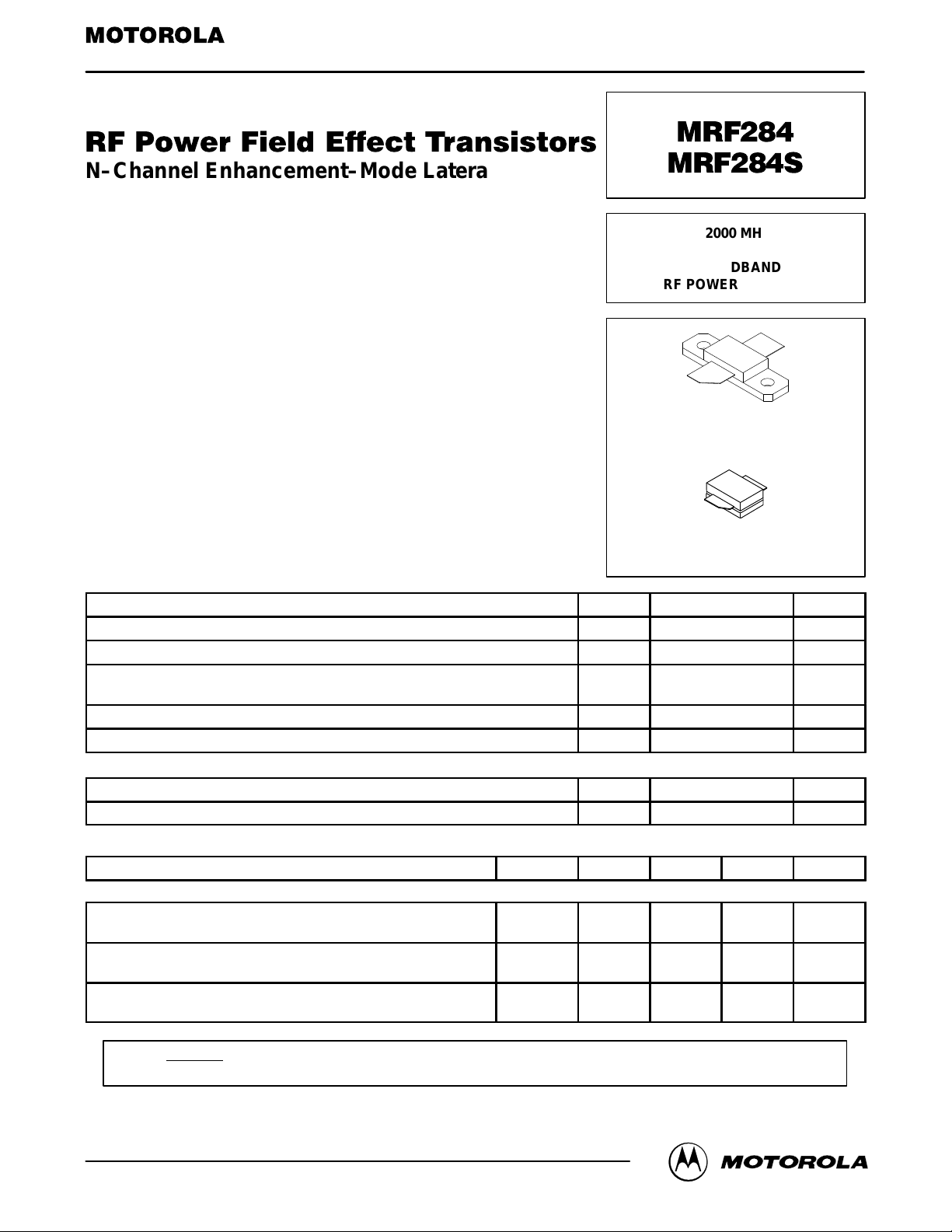
SEMICONDUCTOR TECHNICAL DATA
The RF Sub–Micron MOSFET Line
N–Channel Enhancement–Mode Lateral MOSFETs
Designed for PCN and PCS base station applications at frequencies from
1000 to 2600 MHz. Suitable for FM, TDMA, CDMA, and multicarrier amplifier
applications. To be used in class A and class AB for PCN–PCS/cellular radio
and wireless local loop.
• Specified Two–Tone Performance @ 2000 MHz, 26 Volts
Output Power = 30 Watts (PEP)
Power Gain = 9 dB
Efficiency = 30%
Intermodulation Distortion = –29 dBc
• Typical Single–Tone Performance at 2000 MHz, 26 Volts
Output Power = 30 Watts (CW)
Power Gain = 9.5 dB
Efficiency = 45%
• Characterized with Series Equivalent Large–Signal Impedance Parameters
• S–Parameter Characterization at High Bias Levels
• Excellent Thermal Stability
• Capable of Handling 10:1 VSWR, @ 26 Vdc, 2000 MHz, 30 Watts (CW)
Output Power
Order this document
by MRF284/D
30 W, 2000 MHz, 26 V
LATERAL N–CHANNEL
BROADBAND
RF POWER MOSFETs
CASE 360B–01, STYLE 1
(MRF284)
MAXIMUM RATINGS
Rating Symbol Value Unit
Drain–Source Voltage V
Gate–Source Voltage V
Total Device Dissipation @ TC = 25°C
Derate above 25°C
Storage Temperature Range T
Operating Junction Temperature T
THERMAL CHARACTERISTICS
Characteristic Symbol Max Unit
Thermal Resistance, Junction to Case R
ELECTRICAL CHARACTERISTICS (T
Characteristic
OFF CHARACTERISTICS
Drain–Source Breakdown Voltage
(VGS = 0, ID = 10 µAdc)
Zero Gate Voltage Drain Current
(VDS = 20 Vdc, VGS = 0)
Gate–Source Leakage Current
(VGS = 20 Vdc, VDS = 0)
= 25°C unless otherwise noted)
C
Symbol Min Typ Max Unit
V
(BR)DSS
I
DSS
I
GSS
CASE 360C–03, STYLE 1
(MRF284S)
DSS
GS
P
D
stg
J
θJC
65 — — Vdc
— — 1.0 µAdc
— — 10 µAdc
65 Vdc
±20 Vdc
87.5
0.5
–65 to +150 °C
200 °C
2.0 °C/W
Watts
W/°C
NOTE – CAUTION – MOS devices are susceptible to damage from electrostatic charge. Reasonable precautions in handling and
packaging MOS devices should be observed.
REV 3
Motorola, Inc. 1997
MRF284 MRF284SMOTOROLA RF DEVICE DATA
1

ELECTRICAL CHARACTERISTICS (T
Characteristic Symbol Min Typ Max Unit
ON CHARACTERISTICS
Gate Threshold Voltage
(VDS = 10 Vdc, ID = 150 µAdc)
Gate Quiescent Voltage
(VDS = 26 Vdc, ID = 200 mAdc)
Drain–Source On–Voltage
(VGS = 10 Vdc, ID = 1.0 Adc)
Forward Transconductance
(VDS = 10 Vdc, ID = 1.0 Adc)
DYNAMIC CHARACTERISTICS
Input Capacitance
(VDS = 26 Vdc, VGS = 0, f = 1.0 MHz)
Output Capacitance
(VDS = 26 Vdc, VGS = 0, f = 1.0 MHz)
Reverse Transfer Capacitance
(VDS = 26 Vdc, VGS = 0, f = 1.0 MHz)
FUNCTIONAL TESTS (in Motorola Test Fixture)
Common–Source Power Gain
(VDD = 26 Vdc, P
f1 = 2000.0 MHz, f2 = 2000.1 MHz)
Drain Efficiency
(VDD = 26 Vdc, P
f1 = 2000.0 MHz, f2 = 2000.1 MHz)
Intermodulation Distortion
(VDD = 26 Vdc, P
f1 = 2000.0 MHz, f2 = 2000.1 MHz)
Input Return Loss
(VDD = 26 Vdc, P
f1 = 2000.0 MHz, f2 = 2000.1 MHz)
Common–Source Amplifier Power Gain
(VDD = 26 Vdc, P
f1 = 1930.0 MHz, f2 = 1930.1 MHz)
Drain Efficiency
(VDD = 26 Vdc, P
f1 = 1930.0 MHz, f2 = 1930.1 MHz)
Intermodulation Distortion
(VDD = 26 Vdc, P
f1 = 1930.0 MHz, f2 = 1930.1 MHz)
Input Return Loss
(VDD = 26 Vdc, P
f1 = 1930.0 MHz, f2 = 1930.1 MHz)
Common–Source Amplifier Power Gain
(VDD = 26 Vdc, P
f1 = 2000.0 MHz)
Drain Efficiency
(VDD = 26 Vdc, P
f1 = 2000.0 MHz)
Output Mismatch Stress
(VDD = 26 Vdc, P
f1 = 2000.0 MHz, VSWR = 10:1,
at All Phase Angles)
= 30 W, IDQ = 200 mA,
out
= 30 W, IDQ = 200 mA,
out
= 30 W, IDQ = 200 mA,
out
= 30 W, IDQ = 200 mA,
out
= 30 W PEP, IDQ = 200 mA,
out
= 30 W PEP, IDQ = 200 mA,
out
= 30 W PEP, IDQ = 200 mA,
out
= 30 W PEP, IDQ = 200 mA,
out
= 30 W CW, IDQ = 200 mA,
out
= 30 W CW, IDQ = 200 mA,
out
= 30 W CW, IDQ = 200 mA,
out
C
= 25°C unless otherwise noted)
V
GS(th)
V
GS(q)
V
DS(on)
g
fs
C
iss
C
oss
C
rss
G
ps
η 30 35 — %
IMD — –32 –29 dBc
IRL 9 15 — dB
G
ps
η — 35 — %
IMD — –34 — dBc
IRL 9 15 — dB
G
ps
η 35 45 — %
Ψ
2.0 3.0 4.0 Vdc
3.0 4.0 5.0 Vdc
— 0.3 0.6 Vdc
1.0 1.5 — S
— 43 — pF
— 23 — pF
— 1.4 — pF
9 10.5 — dB
9 10.4 — dB
8.5 9.5 — dB
No Degradation In Output Power
MRF284 MRF284S
2
MOTOROLA RF DEVICE DATA

VGG
+
–
(BIAS)
VDD
C4
B2
R2
B1
+
R1
C1
C7
B3
R3
C5 C8
B4
R4
C15C13
C12
B5
R5
C14
B6
R6
C17
(DC Supply)
+
+
_
L1
RF
INPUT
Z1 Z2 Z3 Z4
C6
C2
C3
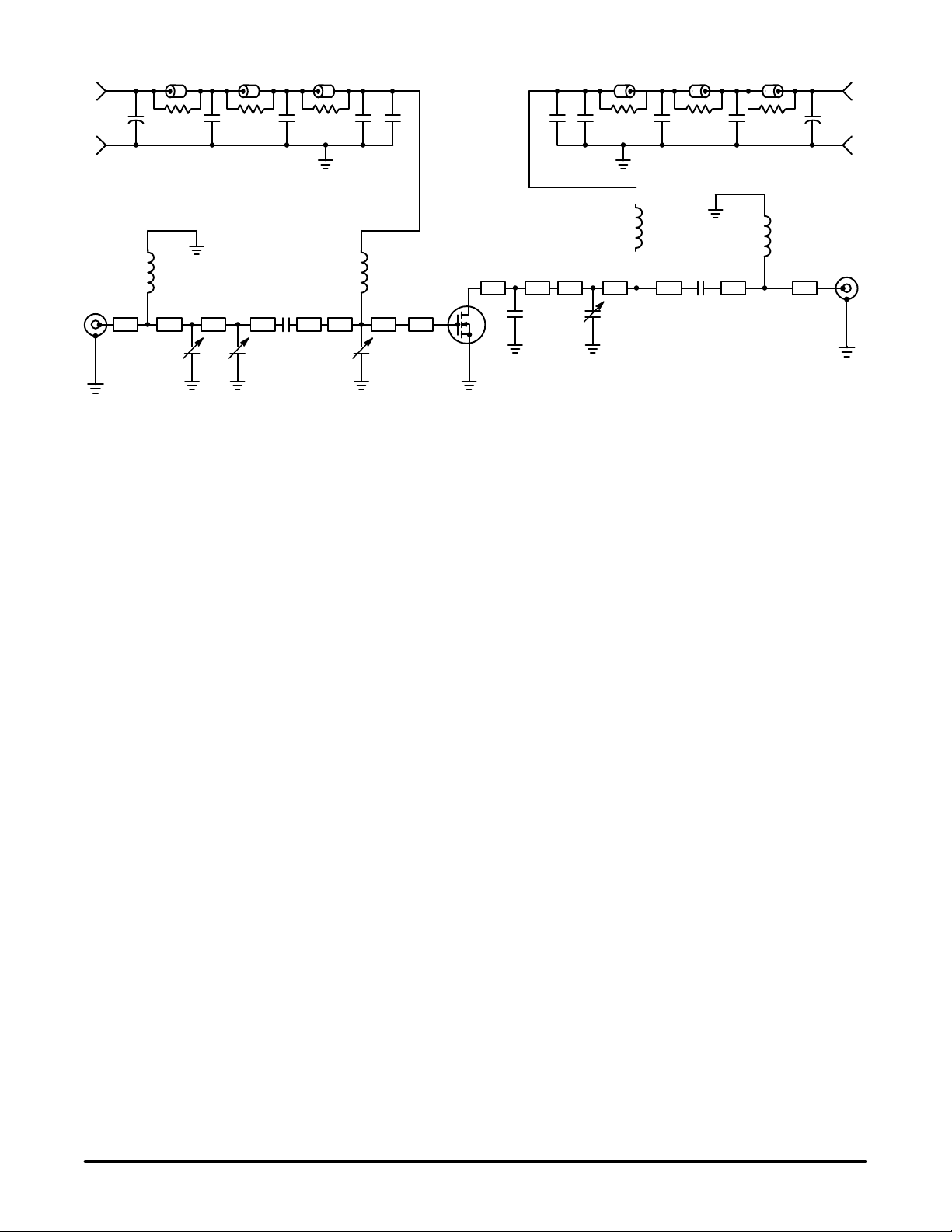
B1 – B6 Ferrite Bead, Round
C1, C17 470 µF, 63 V, Mallory Electrolytic Capacitor
C2 0.6 – 4.5 pF Johansen Gigatrim Variable Capacitors
C3, C9 0.8 – 8.0 pF Johansen Gigatrim Variable Capacitors
C4, C14 0.1 µF Chip Capacitor, KEMET
C5, C15 91 pF ATC RF Chip Capacitors, Case “B”
C6, C16 10 pF ATC RF Chip Capacitors, Case “B”
C7, C12 1000 pF ATC RF Chip Capacitors, Case “B”
C8, C13 5.1 pF ATC RF Chip Capacitors, Case “B”
C10 2.7 pF ATC RF Chip Capacitors, Case “B”
C11 0.4 – 2.5 pF Johansen Gigatrim Variable Capacitors
L1 4 Turns, #27 AWG, 0.087″ OD, 0.050″ ID, 0.069″ Long, 10 nH
L2, L3 9 Turns, #26 AWG, 0.080″ OD, 0.046″ ID, 0.170″ Long, 30.8 nH
L4 2 Turns, #24 AWG, 0.85″ OD, 0.042″ ID, 0.064″ Long, 5.2 nH
R1 – R6 12 Ω Fixed Film Chip Resistor 0.08″ x 0.13″
Z1 0.145″ x 0.080″ Microstrip
Z2 0.680″ x 0.080″ Microstrip
Z5
Z6
L2
Z7 Z8
C9
Z9
DUT
Z10
C10
L3
Z11
Z12 Z13 Z14
C16
C11
Z3 0.185″ x 0.080″ Microstrip
Z4 0.395″ x 0.080″ Microstrip
Z5 0.490″ x 0.080″ Microstrip
Z6 0.035″ x 0.325″ Microstrip
Z7 0.240″ x 0.325″ Microstrip
Z8 0.210″ x 0.515″ Microstrip
Z9 0.130″ x 0.515″ Microstrip
Z10 0.080″ x 0.515″ Microstrip
Z11 0.190″ x 0.325″ Microstrip
Z12 0.090″ x 0.325″ Microstrip
Z13 0.515″ x 0.080″ Microstrip
Z14 0.860″ x 0.080″ Microstrip
Z15 0.510″ x 0.080″ Microstrip
Board 0.030″ Glass Teflon, 2 oz Copper,
3 x 5″ Dimensions, Manufacturer;
Arlon, P/N: GX0300–55–22, εr = 2.55
L4
Z15
RF
OUTPUT
Figure 1. Schematic of 1.93–2.0 GHz Broadband T est Circuit
MRF284 MRF284SMOTOROLA RF DEVICE DATA
3

V
SUPPLY
+
R1
P1
Q1
R2
–
RF
INPUT
R4
L1
Z1 Z2 Z3 Z5
R3
L2
Q2
C3
R5
+
C1
+
V
Z4
DD
R6
+
Z6L3Z7 Z8
C5
B1
R7
C6
C8
Z9
B2
R8
DUT
C2
Z10
C4C7C9
L4
Z11
Z12
C12
B3
R9
Z13 Z15 Z16
Z14
B4
R10B5R11
C14
C15C10C13C11
C17
C16
V
DD
+
+
RF
OUTPUT
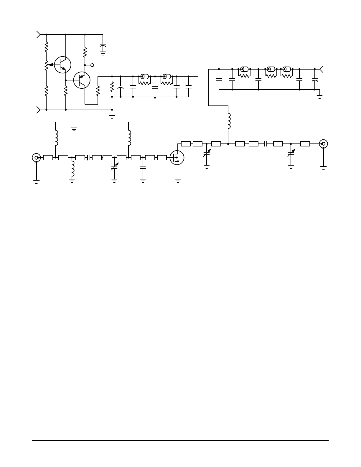
B1 – B5 Ferrite Bead, Round
C1, C9, C16 100 µF, 50 V, Electrolytic Capacitor, Sprague
C2, C13 51 pF, ATC RF Chip Capacitors, Case “B”
C3, C14 10 pF, ATC RF Chip Capacitors, Case “B”
C4, C11 12 pF, ATC RF Chip Capacitors, Case “B”
C5 0.8 – 8.0 pF Variable Capacitor, Johansen Gigatrim
C6 4.7 pF, ATC RF Chip Capacitor, Case “B”
C7, C15 91 pF, ATC RF Chip Capacitors, Case “B”
C8 1000 pF, ATC RF Chip Capacitor, Case “B”
C10 0.1 µF, Chip Capacitor, KEMET
C12, C17 0.6 – 4.5 pF , Variable Capacitors, Johansen Gigatrim
L1 4 Turns, #27 AWG, 0.087″ OD, 0.050″ ID,
0.069″ Long, 10 nH
L2 5 Turns, #24 AWG, 0.083″ OD, 0.040″ ID,
0.128″ Long, 12.5 nH
L3, L4 9 Turns, #26 AWG, 0.080″ OD, 0.046″ ID,
0.170″ Long, 30.8 nH
P1 1000 Ohm Potentiometer , 1/2 W, 10 Turns
Q1 Transistor, NPN, Motorola P/N: MJD31, Case 369A–10
Q2 Transistor, PNP, Motorola P/N: MJD32, Case 369A–10
R1 360 Ω, Fixed Film Chip Resistor 0.08″ x 0.13″
R2 2 x 12 kΩ, Fixed Film Chip Resistor 0.08″ x 0.13″
R3 1 Ω, Wirewound, 5 W, 3% Resistor
R4 4 x 6.8 kΩ, Fixed Film Chip Resistor 0.08″ x 0.13″
Figure 2. Schematic of 2.0 GHz Class A Test Circuit
R5 2 x 1500 Ω, Fixed Film Chip Resistor 0.08″ x 0.13″
R6 270 Ω, Fixed Film Chip Resistor, 0.08″ x 0.13″
R7 – R11 12 Ω, Fixed Film Chip Resistor, 0.08″ x 0.13″
Z1 0.363″ x 0.080″ Microstrip
Z2 0.080″ x 0.080″ Microstrip
Z3 0.916″ x 0.080″ Microstrip
Z4 0.517″ x 0.080″ Microstrip
Z5 0.050″ x 0.325″ Microstrip
Z6 0.050″ x 0.325″ Microstrip
Z7 0.071″ x 0.325″ Microstrip
Z8 0.125″ x 0.325″ Microstrip
Z9 0.210″ x 0.515″ Microstrip
Z10 0.210″ x 0.515″ Microstrip
Z11 0.235″ x 0.325″ Microstrip
Z12 0.02″ x 0.325″ Microstrip
Z13 0.02″ x 0.325″ Microstrip
Z14 0.510″ x 0.080″ Microstrip
Z15 0.990″ x 0.080″ Microstrip
Z16 0.390″ x 0.080″ Microstrip
Raw PCB
Material 0.030″ Glass Teflon, 2 oz Copper,
3 x 5″ Dimensions, Manufacturer;
Arlon, P/N: GX–0300–55–22, εr = 2.55
MRF284 MRF284S
4
MOTOROLA RF DEVICE DATA
 Loading...