Motorola MRF282Z, MRF282S Datasheet

SEMICONDUCTOR TECHNICAL DATA
The RF Sub–Micron MOSFET Line
N–Channel Enhancement–Mode Lateral MOSFETs
Designed for class A and class AB PCN and PCS base station applications at
frequencies up to 2600 MHz. Suitable for FM, TDMA, CDMA, and multicarrier
amplifier applications.
• Specified Two–Tone Performance @ 2000 MHz, 26 Volts
Output Power = 10 Watts (PEP)
Power Gain = 1 1 dB
Efficiency = 30%
Intermodulation Distortion = –30 dBc
• Specified Single–Tone Performance @ 2000 MHz, 26 Volts
Output Power = 10 Watts (CW)
Power Gain = 1 1 dB
Efficiency = 40%
• Characterized with Series Equivalent Large–Signal
Impedance Parameters
• S–Parameter Characterization at High Bias Levels
• Excellent Thermal Stability
• Capable of Handling 10:1 VSWR, @ 26 Vdc,
2000 MHz, 10 Watts (CW) Output Power
• Gold Metallization for Improved Reliability
Order this document
by MRF282/D
10 W, 2000 MHz, 26 V
LATERAL N–CHANNEL
BROADBAND
RF POWER MOSFETs
CASE 458–03, STYLE 1
(MRF282S)
CASE 458A–01, STYLE 1
(MRF282Z)
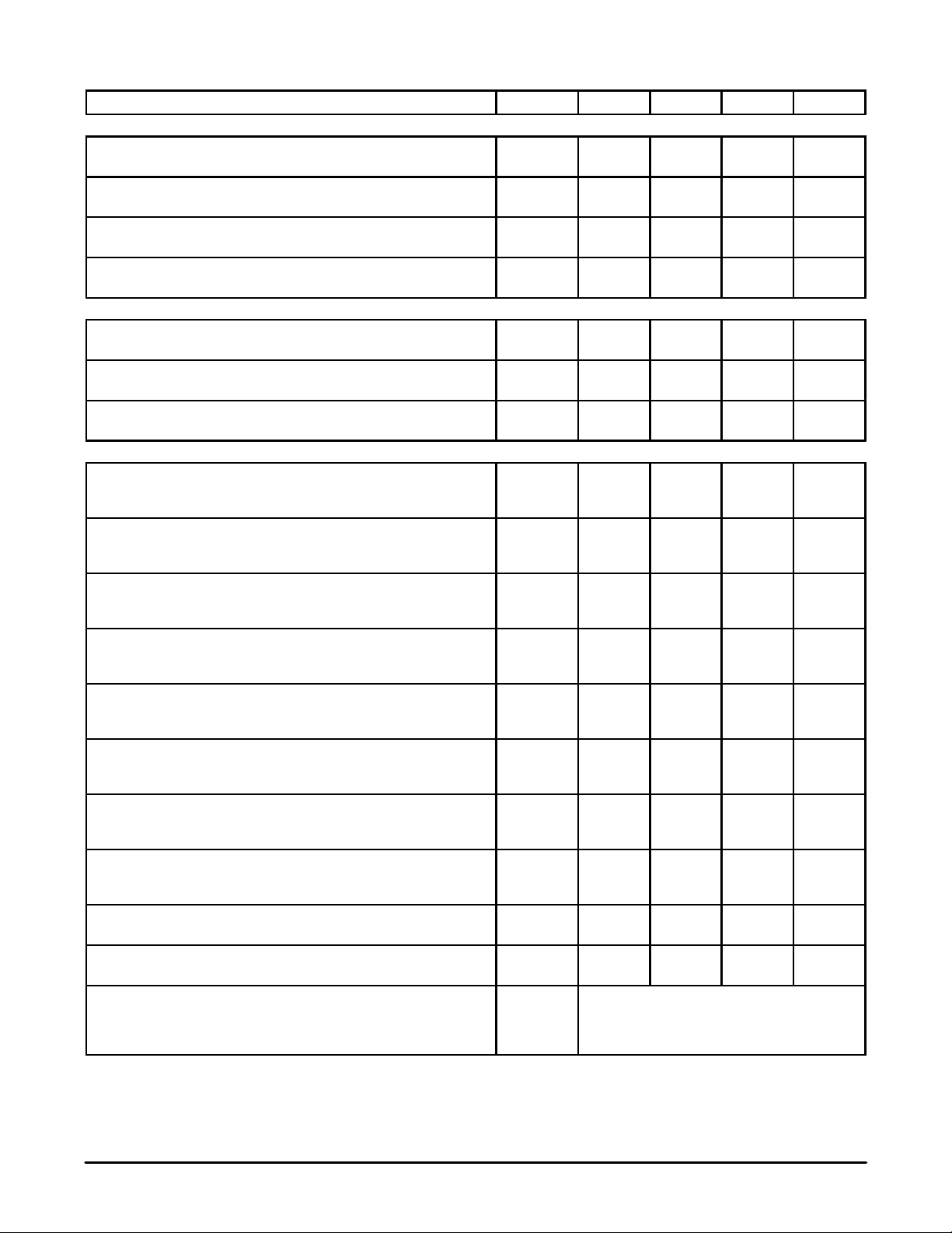
MAXIMUM RATINGS
Rating Symbol Value Unit
Drain–Source Voltage V
Gate–Source Voltage V
Total Device Dissipation @ TC = 25°C
Derate above 25°C
Storage Temperature Range T
Operating Junction Temperature T
THERMAL CHARACTERISTICS
Characteristic Symbol Max Unit
Thermal Resistance, Junction to Case R
ELECTRICAL CHARACTERISTICS (T
Characteristic Symbol Min Typ Max Unit
OFF CHARACTERISTICS
Drain–Source Breakdown Voltage
(VGS = 0, ID = 10 µAdc)
Zero Gate Voltage Drain Current
(VDS = 28 Vdc, VGS = 0)
Gate–Source Leakage Current
(VGS = 20 Vdc, VDS = 0)
= 25°C unless otherwise noted)
C
V
(BR)DSS
I
DSS
I
GSS
DSS
GS
P
D
stg
J
θJC
65 — — Vdc
— — 1.0 µAdc
— — 1.0 µAdc
65 Vdc
±20 Vdc
60
0.34
–65 to +150 °C
200 °C
2.9 °C/W
Watts
W/°C
NOTE – CAUTION – MOS devices are susceptible to damage from electrostatic charge. Reasonable precautions in handling and
packaging MOS devices should be observed.
REV 1
Motorola, Inc. 1997
MRF282S MRF282ZMOTOROLA RF DEVICE DATA
1

ELECTRICAL CHARACTERISTICS continued (T
Characteristic Symbol Min Typ Max Unit
ON CHARACTERISTICS
Gate Threshold Voltage
(VDS = 10 Vdc, ID = 50 µAdc)
Drain–Source On–Voltage
(VGS = 10 Vdc, ID = 0.5 Adc)
Forward Transconductance
(VDS = 10 Vdc, ID = 0.5 Adc)
Gate Quiescent Voltage
(VDS = 26 Vdc, ID = 75 mAdc)
DYNAMIC CHARACTERISTICS
Input Capacitance
(VDS = 26 Vdc, VGS = 0, f = 1.0 MHz)
Output Capacitance
(VDS = 26 Vdc, VGS = 0, f = 1.0 MHz)
Reverse Transfer Capacitance
(VDS = 26 Vdc, VGS = 0, f = 1.0 MHz)
FUNCTIONAL TESTS (In Motorola Test Fixture)
Common–Source Power Gain
(VDD = 26 Vdc, P
f1 = 2000.0 MHz, f2 = 2000.1 MHz)
Drain Efficiency
(VDD = 26 Vdc, P
f1 = 2000.0 MHz, f2 = 2000.1 MHz)
Intermodulation Distortion
(VDD = 26 Vdc, P
f1 = 2000.0 MHz, f2 = 2000.1 MHz)
Input Return Loss
(VDD = 26 Vdc, P
f1 = 2000.0 MHz, f2 = 2000.1 MHz)
Common–Source Power Gain
(VDD = 26 Vdc, P
f1 = 1930.0 MHz, f2 = 1930.1 MHz)
Drain Efficiency
(VDD = 26 Vdc, P
f1 = 1930.0 MHz, f2 = 1930.1 MHz)
Intermodulation Distortion
(VDD = 26 Vdc, P
f1 = 1930.0 MHz, f2 = 1930.1 MHz)
Input Return Loss
(VDD = 26 Vdc, P
f1 = 1930.0 MHz, f2 = 1930.1 MHz)
Common–Source Power Gain
(VDD = 26 Vdc, P
Drain Efficiency
(VDD = 26 Vdc, P
Output Mismatch Stress
(VDD = 26 Vdc, P
f1 = 2000.0 MHz, f2 = 2000.1 MHz, Load VSWR = 10:1,
All Phase Angles at Frequency of Test)
= 10 W (PEP), IDQ = 75 mA,
out
= 10 W (PEP), IDQ = 75 mA,
out
= 10 W (PEP), IDQ = 75 mA,
out
= 10 W (PEP), IDQ = 75 mA,
out
= 10 W (PEP), IDQ = 75 mA,
out
= 10 W (PEP), IDQ = 75 mA,
out
= 10 W (PEP), IDQ = 75 mA,
out
= 10 W (PEP), IDQ = 75 mA,
out
= 10 W CW, IDQ = 75 mA, f = 2000.0 MHz)
out
= 10 W CW, IDQ = 75 mA, f = 2000.0 MHz)
out
= 10 W CW, IDQ = 75 mA,
out
= 25°C unless otherwise noted)
C
V
GS(th)
V
DS(on)
g
fs
V
GS(q)
C
iss
C
oss
C
rss
G
ps
η 30 34 — %
I
MD
I
RL
G
ps
η — 30 — %
I
MD
I
RL
G
ps
η 40 45 — %
Ψ
2.0 3.0 4.0 Vdc
— 0.4 0.6 Vdc
0.5 0.7 — S
3.0 4.0 5.0 Vdc
— 15 — pF
— 8.0 — pF
— 0.45 — pF
11 12.6 — dB
— –32.5 –30 dBc
10 14 — dB
11 12.6 — dB
— –32.5 — dBc
10 14 — dB
11 12.3 — dB
No Degradation In Output Power
MRF282S MRF282Z
2
MOTOROLA RF DEVICE DATA

V
GG
INPUT
+
C1
RF
C2 C4
B1
R1
Z1 Z2 Z3 Z4 Z5
L1
C3
B2
R2
C6
L2
C5
B3
R3
C7
C8
C9
Z6
B4
C10
C11
R4
L3
Z7 Z9
C12
DUT
C14
Z8
B5
R5
C13
C15
L4
B6
R6
Z10
+
C17
C16
V
DD
RF
OUTPUT
B1, B2, B3, Ferrite Bead, Ferroxcube, 56–590–65–3B
B4, B5, B6
C1, C17 470 µF, Electrolytic Capacitor, Mallory
C2, C4, C12 0.6–4.5 pF , Variable Capacitor, Johanson
C3, C15 0.1 µF, Chip Capacitor, Kemet
C5, C14 1000 pF, B Case Chip Capacitor, ATC
C6, C8, C10, C13 12 pF, B Case Chip Capacitor, ATC
C7 1.8 pF, B Case Chip Capacitor, ATC
C9, C11 100 pF, B Case Chip Capacitor, ATC
C16 0.4–2.5 pF, Variable Capacitor, Johanson
L1 Straight Wire, 21 AWG, 0.3″
L2 8 Turns, 0.042″ ID, 24 A WG, Enamel
L3 9 Turns, 0.046″ ID, 26 A WG, Enamel
L4 3 Turns, 0.048″ ID, 25 A WG, Enamel
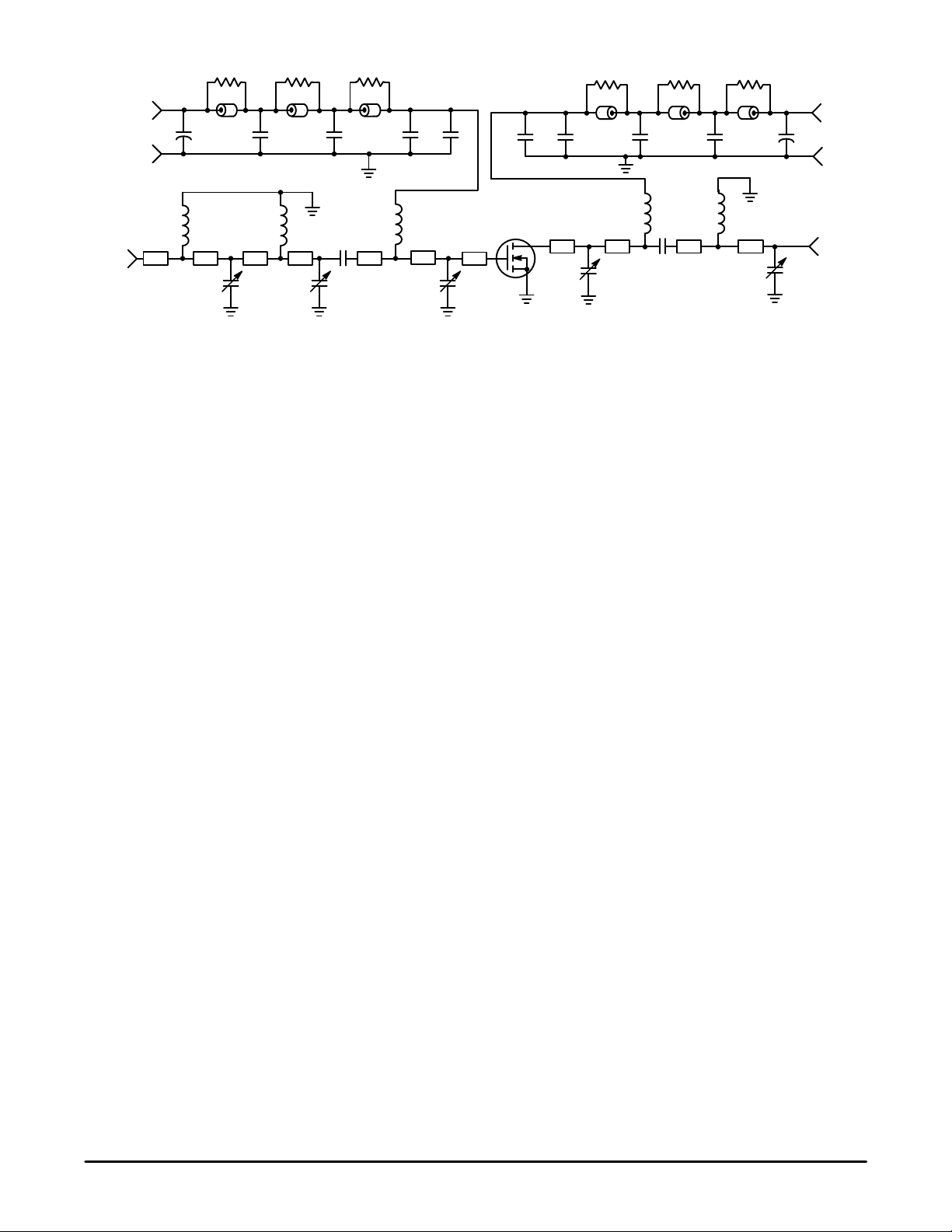
Figure 1. Schematic of 1.93 – 2.0 GHz Broadband T est Circuit
R1, R2, R3, 12 Ω, 0.2 W Chip Resistor, Rohm
R4, R5, R6
Z1 0.155″ x 0.08″ Microstrip
Z2 0.280″ x 0.08″ Microstrip
Z3 0.855″ x 0.08″ Microstrip
Z4 0.483″ x 0.08″ Microstrip
Z5 0.200″ x 0.330″ Microstrip
Z6 0.220″ x 0.330″ Microstrip
Z7 0.490″ x 0.330″ Microstrip
Z8 0.510″ x 0.08″ Microstrip
Z9 0.990″ x 0.08″ Microstrip
Z10 0.295″ x 0.08″ Microstrip
Board 35 Mils Glass Teflon, Arlon GX–300,
εr = 2.55
Input/Output Connectors Type N Flange Mount
MRF282S MRF282ZMOTOROLA RF DEVICE DATA
3

RF
INPUT
R1
+
V
GG
(BIAS)
+
B1
C1
–
L1
Z1 Z2 Z3 Z4 Z5
C2 C3
L2
C4
R2
B2
C6
C7
R3
B3
C5 C8
L3
Z6
C9
Z7
DUT
L5
R6
B6
Z11
C16
+
C17
DC
SUPPLY
+
V
DD
–
RF
OUTPUT
R4
B5
C11C14
Z8
C12
C10
Z9
L4
C15
R5
B4
C13
Z10
B1, B2, B3, Ferrite Bead, Fair Rite, (2743021446)
B4, B5, B6
C1, C16 470 µ F, 63 V, Electrolytic Capacitor, Mallory
C2, C9, C12 0.6–4.5 pF, Variable Capacitor, Johanson Gigatrim
C3 0.8–4.5 pF, Variable Capacitor, Johanson Gigatrim
C4, C13 0.1 µF, Chip Capacitor
C5, C14 100 pF, B Case Chip Capacitor, ATC
C6, C8, C11, C15 12 pF, B Case Chip Capacitor, ATC
C7, C10 1000 pF, B Case Chip Capacitor, ATC
C17 0.1 pF, B Case Chip Capacitor, ATC
L1 3 Turns, 27 AWG, 0.087″ OD, 0.050″ ID,
0.053″ Long, 6.0 nH
L2 5 Turns, 27 AWG, 0.087″ OD, 0.050″ ID,
0.091″ Long, 15 nH
L3, L4 9 Turns, 26 AWG, 0.080″ OD, 0.046″ ID,
0.170″ Long, 30.8 nH
L5 4 Turns, 27 AWG, 0.087″ OD, 0.050″ ID,
0.078″ Long, 10 nH
Figure 2. Schematic of 1.81 – 1.88 GHz Broadband T est Circuit
R1, R2, R3, 12 Ω, 1/8 W Fixed Film Chip Resistor,
R4, R5, R6 0.08″ x 0.13″
W1, W2 Berrylium Copper, 0.010″
Z1 0.122″ x 0.08″ Microstrip
Z2 0.650″ x 0.08″ Microstrip
Z3 0.160″ x 0.08″ Microstrip
Z4 0.030″ x 0.08″ Microstrip
Z5 0.045″ x 0.08″ Microstrip
Z6 0.291″ x 0.08″ Microstrip
Z7 0.483″ x 0.330″ Microstrip
Z8 0.414″ x 0.330″ Microstrip
Z9 0.392″ x 0.08″ Microstrip
Z10 0.070″ x 0.08″ Microstrip
Z11 1.110″ x 0.08″ Microstrip
Board 1 = 0.03 Glass Teflon, Arlon GX–0300–55–22,
2 oz Copper, 3 x 5″ Dimenson, 0.030″,
x 0.110″x 0.210
εr = 2.55
″
MRF282S MRF282Z
4
MOTOROLA RF DEVICE DATA
 Loading...